EP0025606B1 - Apparatus for compensation of overshoot, undershoot and delay in response to step signals in a system comprising a reactive filter network - Google Patents
Apparatus for compensation of overshoot, undershoot and delay in response to step signals in a system comprising a reactive filter network Download PDFInfo
- Publication number
- EP0025606B1 EP0025606B1 EP80105534A EP80105534A EP0025606B1 EP 0025606 B1 EP0025606 B1 EP 0025606B1 EP 80105534 A EP80105534 A EP 80105534A EP 80105534 A EP80105534 A EP 80105534A EP 0025606 B1 EP0025606 B1 EP 0025606B1
- Authority
- EP
- European Patent Office
- Prior art keywords
- input
- output
- coupled
- signal
- filter
- Prior art date
- Legal status (The legal status is an assumption and is not a legal conclusion. Google has not performed a legal analysis and makes no representation as to the accuracy of the status listed.)
- Expired
Links
- 230000004044 response Effects 0.000 title claims description 35
- 239000003990 capacitor Substances 0.000 claims description 36
- 230000002441 reversible effect Effects 0.000 claims description 23
- 230000008859 change Effects 0.000 claims description 17
- 230000001105 regulatory effect Effects 0.000 claims description 11
- 238000012937 correction Methods 0.000 claims description 9
- 230000008878 coupling Effects 0.000 claims 1
- 238000010168 coupling process Methods 0.000 claims 1
- 238000005859 coupling reaction Methods 0.000 claims 1
- 238000010586 diagram Methods 0.000 description 10
- 230000000694 effects Effects 0.000 description 9
- 238000007599 discharging Methods 0.000 description 5
- 230000010355 oscillation Effects 0.000 description 4
- 230000008901 benefit Effects 0.000 description 3
- 230000007423 decrease Effects 0.000 description 3
- 230000003111 delayed effect Effects 0.000 description 3
- 230000001052 transient effect Effects 0.000 description 3
- 238000012935 Averaging Methods 0.000 description 2
- 239000013078 crystal Substances 0.000 description 2
- 238000013016 damping Methods 0.000 description 2
- 238000013461 design Methods 0.000 description 2
- 238000001208 nuclear magnetic resonance pulse sequence Methods 0.000 description 2
- 238000011084 recovery Methods 0.000 description 2
- 230000001133 acceleration Effects 0.000 description 1
- 230000009471 action Effects 0.000 description 1
- 230000001276 controlling effect Effects 0.000 description 1
- 230000003247 decreasing effect Effects 0.000 description 1
- 230000001934 delay Effects 0.000 description 1
- 230000001419 dependent effect Effects 0.000 description 1
- 238000006073 displacement reaction Methods 0.000 description 1
- 230000010354 integration Effects 0.000 description 1
- 238000012423 maintenance Methods 0.000 description 1
- 238000012986 modification Methods 0.000 description 1
- 230000004048 modification Effects 0.000 description 1
- 230000003287 optical effect Effects 0.000 description 1
- 230000010363 phase shift Effects 0.000 description 1
- 230000009467 reduction Effects 0.000 description 1
- 238000009738 saturating Methods 0.000 description 1
- 230000005236 sound signal Effects 0.000 description 1
- 230000001629 suppression Effects 0.000 description 1
- 230000001360 synchronised effect Effects 0.000 description 1
Images


Classifications
-
- G—PHYSICS
- G11—INFORMATION STORAGE
- G11B—INFORMATION STORAGE BASED ON RELATIVE MOVEMENT BETWEEN RECORD CARRIER AND TRANSDUCER
- G11B5/00—Recording by magnetisation or demagnetisation of a record carrier; Reproducing by magnetic means; Record carriers therefor
- G11B5/48—Disposition or mounting of heads or head supports relative to record carriers ; arrangements of heads, e.g. for scanning the record carrier to increase the relative speed
- G11B5/58—Disposition or mounting of heads or head supports relative to record carriers ; arrangements of heads, e.g. for scanning the record carrier to increase the relative speed with provision for moving the head for the purpose of maintaining alignment of the head relative to the record carrier during transducing operation, e.g. to compensate for surface irregularities of the latter or for track following
- G11B5/596—Disposition or mounting of heads or head supports relative to record carriers ; arrangements of heads, e.g. for scanning the record carrier to increase the relative speed with provision for moving the head for the purpose of maintaining alignment of the head relative to the record carrier during transducing operation, e.g. to compensate for surface irregularities of the latter or for track following for track following on disks
- G11B5/59627—Aligning for runout, eccentricity or offset compensation
-
- G—PHYSICS
- G05—CONTROLLING; REGULATING
- G05B—CONTROL OR REGULATING SYSTEMS IN GENERAL; FUNCTIONAL ELEMENTS OF SUCH SYSTEMS; MONITORING OR TESTING ARRANGEMENTS FOR SUCH SYSTEMS OR ELEMENTS
- G05B5/00—Anti-hunting arrangements
- G05B5/01—Anti-hunting arrangements electric
-
- G—PHYSICS
- G05—CONTROLLING; REGULATING
- G05D—SYSTEMS FOR CONTROLLING OR REGULATING NON-ELECTRIC VARIABLES
- G05D3/00—Control of position or direction
- G05D3/12—Control of position or direction using feedback
- G05D3/14—Control of position or direction using feedback using an analogue comparing device
- G05D3/1445—Control of position or direction using feedback using an analogue comparing device with a plurality of loops
Definitions
- the invention relates to apparatus for compensation of overshoot, undershoot and delay in response to stop signals in a system utilizing filter networks with reactive components.
- Filter networks having reactive components are known to provide overshoot or undershoot transients in response to sudden D.C. signal level changes applied thereto. These transients, in turn, add to the delay in the filter response. Even in critically damped filters, which do not exhibit such overshoot or undershoot transients, a delay in response to sudden D.C. level changes occurs due to recovery time necessary for adjusting the reactive elements of the filter to a new D.C. signal level.
- Prior art servo circuits compensate for the above effects by reducing the gain of the servo loop to minimize oscillations. The result is a servo operating below the optimum loop gain and, thus, with reduced accuracy.
- FIG. 1 An example of a prior art device comprising a positioning servo circuit is described in the operation and Maintenance Manual, DM 940/DM 980 Disk Storage Drive, No. 3306685-01, issued October 1977, by Ampex Corporation, the present applicant. More particularly, Figure 3-4 on page 3-9 of that Manual shows a basic servo block diagram, including a fine mode positioning servo control circuit. The latter circuit is utilized for maintaining the transducer assembly of the disk storage within a designated track location until a subsequent coarse positioning mode is initiated, as it is known in the art. As it is shown, for example, in the detailed circuit diagram No.
- an offset forward or reverse signal may be applied by the control electronics to the servo.
- the latter respective signals are negative or positive D.C. voltage steps injected in the servo loop, which serve to move the servo head and, thus, the entire head assembly slightly in either direction with respect to the center of the servo track in order to maximize the signal obtained from the recorded data tracks with respect to the playback heads.
- the gain of the servo amplifier has been selected relatively low to minimize servo oscillations, overshoot or undershoot in response to the D.C. offset forward or reverse signal.
- One embodiment of the present invention overcomes the above-described disadvantages of prior art positioning servo circuits by providing a reactive filter circuit which allows for increasing the servo loop gain and bandwidth, in combination with a circuit for compensation of overshoot and undershoot transients and delay in response to D.C. signal level changes applied to the reactive filter circuit, as it will be disclosed in the description in more detail.
- a passive or active filter comprising one or more reactive elements which may be combined with resistive or other filter elements and having at least one filter element coupled between an input, an output and a signal return line of the filter.
- a circuit for automatic compensation of overshoot and undershoot transients and delay in response to D.C. signal steps applied to circuits utilizing reactive filters.
- the compensation circuit detects an input step signal applied to the reactive filter, and it provides a compensation step signal and applies it to the return line of the filter, simultaneously with the input step signal received by the filter.
- the compensation signal is substantially of the same magnitude and of a predetermined polarity with respect to the input step signal to compensate for a resulting signal level change with respect to the reactive filter.
- Fig. 4 is a block diagram showing a still further embodiment of the invention utilized in a regulated switching power supply circuit.
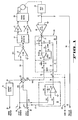
- Fig. 1 The preferred embodiment of the invention shown in Fig. 1 is utilized in a position and velocity servo of a disk storage drive system, manufactured by the present applicant.
- the block diagram of Fig. 1 comprises known basic servo circuit components, such as shown and described in the previously indicated Manual, in combination with the reactive filter circuit 28 and compensation circuit 10 in accordance with the teachings of the present invention. Consequently, only those portions of the basic servo system will be shown and described in the following specification, which are necessary to understand the operation and advantages of the invention.
- the circuit of Fig. 1 comprises an error amplifier 12 utilized during both the coarse and fine positioning modes of the servo circuit.
- the error amplifier 12 receives via line 50 at its inverting (-) input a forward or reverse current, which is applied from a current source 11 via line 34 and a summing junction 30.
- the input of the current source 11 is coupled to terminal 35, where it receives a digital signal from a difference counter (not shown), indicating the number of cylinder tracks to be crossed in either direction to obtain the desired position of the head assembly 24 with respect to the disk surface.
- the polarity and number of bits representing the digital signal is determined by a difference calculator (not shown), and is dependent on the actual cylinder track location of the servo head and a desired cylinder track location, to which the head has to move.
- the forward or reverse current causes the output signal of the error amplifier 12 to increase or decrease.
- a polarity detector 14 whose input is coupled via line 13 to the output of error amplifier 12, drives a forward amplifier 16 and a reverse amplifier 18, respectively, depending on the output signal polarity of the error amplifier 12.
- the respective output signal from the forward or reverse amplifier 16 or 18 is applied to a power driver 20, which in turn causes current to flow through a voice coil of linear motor 22 in either direction.
- the motor 22 moves the head carriage (not shown) to which the head assembly 24 including the data heads and servo head is attached.
- the servo head supplies via line 39 and terminal 40 position feedback information indicating cylinder track crossings to the difference counter (not shown), which information updates, that is decrements, the difference counter. Consequently, the digital signal applied to the input terminal 35 is also decremented, until the difference count is zero and no current is applied from the current source 11 to the error amplifier 12; thus, indicating that the servo head has completed its move in the coarse positioning mode, and the head assembly 24 has reached the desired cylinder track location.
- Switch S1 connects the fine positioning servo loop, including the position amplifier 26, reactive filter network 28 and summing resistor R84 between the servo head output 32 and the summing junction 30.
- Switch S3 connects the voltage reference line 53 of filter 28, also referred to as voltage or signal return line, to the output 58 of the compensation circuit 10, which circuit will be described later. In the fine positioning mode the position of the head assembly 24 is maintained on the designated track location, until a subsequent coarse positioning mode is initiated as it is known in the art.
- the position amplifier 26 receives a position feedback signal in the form of a continuously varying signal via line 32 from the servo head located in the head assembly 24, indicating the magnitude and polarity of the servo head offset with respect to the center of the servo track.
- the position feedback signal is amplified by the position amplifier 26.
- that amplified signal is applied via a summing junction to the error amplifier input.
- the position feedback signal from amplifier 26 is filtered by the reactive filter network 28, designed in accordance with the present invention as it will be described later in more detail.
- the filtered signal is applied from filter network 28 via output 33 thereof, summing resistor R84 and switch S1 to the summing junction 30 and, from there, to the inverting (-) input 50 of error amplifier 12.
- the combination of the reactive filter network 28 with the compensation circuit 10 in accordance with the teachings of the present invention is utilized to maximize the phase margin, bandwidth and, thus, the gain and positioning accuracy of the servo loop, and to maintain the maximum position accuracy when a D.C. offset forward or reverse signal is received by the servo circuit, as it will be disclosed below in detail.
- reactive filter 28 comprises a phase correction network 29 for providing phase margin in the servo loop and a gain roll-off filter network 31 for reducing the servo gain to a safe level at frequencies close to mechanical resonance, by providing a sharp attenuation in that region.
- the phase correction network 29 comprises a non-inverting operational amplifier 37, having a feedback resistor R5 connected between its inverting (-) input and output.
- a series combination of capacitor C1 and resistor R1, connected in parallel to resistor R2, is coupled to non-inverting input (+) of amplifier 37.
- the above combination of elements form a differentiating circuit, providing phase lead and high gain at high frequencies.
- a series combination of resistor R3 and capacitor C2 connected between the non-inverting input (+) of operational amplifier 37 and the voltage reference line 53 of filter 28, form in combination with amplifier 37 an integrating circuit providing phase lag and high gain at low frequencies.
- phase correction network 29 provides a phase margin necessary to achieve optimum servo stability and damping for the selected servo bandwidth, as determined by the design requirements.
- the roll-off filter 31 is implemented by parallel combination of an inductor L1 and capacitor C4, which combination is in series with resistor R6.
- the above combination of elements is coupled to the output of operational amplifier 37, utilized in the phase correction network 29.
- Capacitor C5 is connected between the output terminal of resistor R6 and the voltage return line 53 of the filter circuit 28 to provide gain roll-off at frequencies beyond the frequency range of the servo.
- the roll-off filter 31 connected to the output of operational amplifier 37, effects a desired minimum loss of the phase margin by providing a sharp attenuation in the region of the mechanical resonances, thus reducing the servo gain to a safe level in that frequency region.
- the attenuation is stopped at a suitable level by voltage divider action of capacitors C4 and C5. The above attenuation level still provides adequate suppression of remaining resonant peaks.
- the known basic servo circuit of Fig. 1 receives an offset forward or offset reverse signal applied to obtain a maximum signal level by the data playback heads from recorded data tracks, as it has been mentioned previously. More particularly, if the maximum signal level obtained at playback from the recorded data tracks does not correspond to the center of the corresponding prerecorded servo track, an offset forward or reverse signal represented by a D.C. voltage step of a predetermined magnitude and polarity is applied in input terminal 36 or 38 by an offset forward or offset reverse latch (not shown) as it is known from the above-referenced Manual.
- an offset forward or reverse signal represented by a D.C. voltage step of a predetermined magnitude and polarity
- the received voltage step is applied via summing resistor R10 or R11 to summing junction 30 where it is combined with the previously described fine position feedback signal obtained from the reactive filter 28 via summing resistor R84.
- the error amplifier 12 thus produces a position error signal at its output 13, with respect to a new reference D.C. voltage level responsive to the offset forward or reverse signal. From the previous description of the servo loop it follows that, as a result, the head assembly 24 will be moved by the linear motor 22 to a corresponding forward or reverse offset position with respect to the center of the servo track, in which position the data picked up by the playback heads will be at maximum signal level. This new offset position will be maintained by the servo loop, until the offset forward or reverse signal at the input 36 or 38 is either removed, or alternatively, changed to an offset signal of opposite polarity.
- the sudden displacement of the servo head to the new offset position effects a sudden change in the D.C. voltage level of the position feedback signal from amplifier 26, which change is sensed as a D.C. step voltage by the input 27 of the reactive filter circuit 28.
- the reactive filter elements cannot charge or discharge instantly to the new D.C. level, due to well known inherent properties of these elements, a delayed filter response would result, which, in turn, would effect overshoot or undershoot transients at output 33 of the filter network 28, as it has been previously discussed. That, in turn, would cause overshoot or undershoot and, thus, related oscillations of the servo head position and delayed lock-on with respect to the servo track.
- the compensation circuit 10 comprises an inverting operational amplifier 51, having a feedback resistor R15 in parallel with feedback capacitor C15 and two input resistors R16, R17, respectively.
- Each input resistor R16, R17 has one terminal coupled to the inverting (-) input of the amplifier 51.
- the other terminal of input resistor R16 is coupled via line 16 to the previously described terminal 36 for receiving the offset forward signal.
- the other terminal of input resistor R17 is coupled via line 17 to previously described input terminal 38 for receiving the offset reverse signal.
- the output 58 of amplifier 51 is coupled via switch S3 to the voltage return line 53 of the reactive filter network 28.
- the non-inverting (+) input terminal of amplifier 51 is grounded. During normal operation in the fine positioning mode, when no position offset signal is received at terminal 36 or 38, the voltage return line 53 of filter 28 is held at ground level via switch S3 and amplifier 51.
- the latter signal closes switch S3, simultaneously with switch S1, when the fine positioning mode is initiated by the servo circuit, as described previously.
- the parameters of the compensation circuit 10 are selected such that the voltage step at output 58, referred to as compensating voltage step or step voltage, is of the same magnitude and polarity as the previously described corresponding input voltage step applied by positioning amplifier 26 to the input 27 of filter 28, to compensate for the latter.
- Capacitor C15 acts as an integrating capacitor across amplifier 51, and its parameters are selected to provide a delay in both the offset forward and reverse signal path, respectively, from terminal 36 or 38 to the output 58 of amplifier 51, to match the delay resulting from the passage of the particular offset signal through a portion of the previously described fine positioning servo circuit, including the summing resistor R10 or R11; error amplifier 12; polarity detector 14; forward or reverse amplifier 16 or 18; power driver 20, motor 22; servo head of assembly 24; and position amplifier 26. Since the offset signal passing through the above-indicated signal path is inverted by the error amplifier 12, respective voltage steps of the same polarity and magnitude are applied simultaneously to both the voltage return line 53 and to the input 27 of filter 28.
- the voltage return line 53 of the reactive filter 28 closely follows the D.C. voltage level changes applied to the filter input, thus effectively compensating for these changes with respect to the reactive filter. Consequently, a substantially constant D.C. voltage level is maintained between the input and return line of the filter, thus preventing the reactive filter elements from charging and discharging and from saturating the filter amplifier in response to the offset forward or reverse signal.
- the above-disclosed combination of the compensation circuit 10 with the reactive filter network 28, in accordance with the preferred embodiment of Fig. 1 of the invention allows a continuous fine positioning servo operation, without undesirable overshoot and undershoot transients and delay in response to D.C. offset signals received by the servo. It will be further appreciated that utilization of the compensation circuit 10, in combination with filter 28, coupled in the position feedback loop of the circuit of Fig. 1 allows increasing the overall servo loop gain in the positioning mode when comparing to prior art servos.
- the recording track density may be doubled when comparing to the prior art disk storage drives.
- utilization of the invention allows a corresponding increase in the positioning accuracy twofold with respect to the resulting narrow tracks.
- the compensation circuit of Fig. 1 may comprise a plurality of input resistors, such as R16, R17, each for receiving a respective voltage step.
- Fig. 2 shows an alternative embodiment of the invention utilized in a capstan servo circuit of a magnetic tape drive, such as known from the PR-2200 series Instrumentation Recorders, manufactured by the present applicants.
- a phase comparator 60 receives at a first input 62 a reference frequency signal, for example, a 100 KHz square wave from a crystal-controlled oscillator (not shown) and a tachometer feedback signal at a second input 64 from the tape drive.
- a reference frequency signal for example, a 100 KHz square wave from a crystal-controlled oscillator (not shown) and a tachometer feedback signal at a second input 64 from the tape drive.
- an off-tape signal from a reproduce amplifier may be received at input 64, indicating tape speed as it is known in the art.
- the tachometer signal is obtained from an optical assembly, comprising a tachometer disc 73, rotating synchronously with the motor 72 and illuminated by light source 71, the velocity of rotation being sensed by detector 75.
- the detector 75 transforms the received light into an electric signal.
- the latter signal is amplified by operational amplifier 76 and subsequently fed back to input 64 of comparator 60.
- the phase comparator 60 compares the frequency and phase of its respective input signals at 62 and 64 and it provides an error signal in the form of a variable duty cycle square wave at output 65.
- the error signal from 65 is applied via a reactive filter network 57, comprising carrier filter 66 and phase lead-lag network 69, to motor amplifier 70.
- the carrier filter 66 comprises inductor L8, capacitor C8 and resistor R7 in a combination providing integration of the square wave output signal of the comparator 60, to obtain an error signal free of the carrier frequency.
- the phase lead-lag network 69 comprises resistors R8, R9, R12 and capacitors C6, C7 combined to provide a phase lead to stabilize the particular servo loop of the preferred embodiment of Fig. 2.
- the magnitude and polarity of the output signal of amplifier 70 is responsive to the error signal and it controls the rotational speed of motor 72 to compensate for deviations of the motor speed from the reference signal frequency.
- Examples of detailed circuit diagrams of both the digital phase comparator 60 and synchronism detector 67 are shown in Fig. 2, and are known from the above-mentioned prior art PR-2200 series recorders.
- the phase comparator 60 comprises three binary flip-flop stages U10, U11 and U12 connected in tandem, for example, type MC 850 P, manufactured by Motorola Corporation.
- the output Q of binary stage U11 forms the output 65 of the phase comparator 60.
- Output 65 is connected to the input 61 of filter network 57.
- Output 65 of comparator 60 is also connected to the input 68 synchronism detector 67.
- the synchronism detector 67 comprises a one-shot multivibrator chip U3, for example, type 74123, manufactured by Texas Instruments Corporation, for detecting synchronism in the capstan servo drive.
- the output 65 of phase comparator 60 ideally generates a 50 percent duty cycle, as it is known in the art.
- the synchronism detector 67 in response generates a corresponding output signal at 80, in the form of a logic high pulse, as known in the art. The latter pulse is utilized in the circuit of Fig. 2 as an input signal applied to the compensation circuit 10. Since the D.C.
- amplifier 70 receives the filtered error signal from the reactive filter network 57 and in response thereto it applies a driving control current of a corresponding magnitude and polarity causing the capstan motor 72 to accelerate or decelerate accordingly, in order to reduce the error signal.
- the feedback signal from detector 75 is applied via operational amplifier 76 to the feedback input 64 of the phase comparator 60, as previously mentioned.
- the feedback signal frequency at input 64 gradually increases or decreases until the latter signal is of the same frequency and polarity as the reference signal at input 62 of the phase comparator 60, that is, in the above-mentioned example, equal to 100 KHz.
- the circuit of Fig. 2 comprises an automatic compensation circuit 10 having an inverting operational amplifier 51, with an input resistor R18 and feedback resistor R15 in parallel with feedback capacitor C15.
- the inverting (-) input of amplifier 51 is coupled via input resistor R18 and a movable contact 83 of potentiometer 81 to output 80 of the synchronism detector 67.
- Potentiometer 81 has its respective terminals coupled between output 80 of synchronism detector and ground.
- the output 58 of inverting amplifier 51 is connected to the voltage reference line 59 of filter network 57, in a similar manner as it has been shown and previously described with respect to Fig. 1. As it is seen in Fig. 2, the return line 59 is held at ground level via the non-inverting (+) input of operational amplifier 51 when no signal is received at input 82 of circuit 10.
- a negative D.C. voltage step indicating the resulting change to 50% duty cycle square wave at 65 is sensed by the one-shot multivibrator U3 of the synchronism detector 67, which, in turn, provides a logic high pulse at its output 80, as previously described.
- the latter pulse is applied to input 82 of the compensation circuit 10, via potentiometer 81, serving as a voltage divider to adjust the amplitude of the input pulse at 82.
- the potentiometer 81 may be deleted and the output 80 of the synchronism detector 67 connected directly to input 82 of the circuit 10.
- Integrating capacitor C15 is utilized to delay a compensating voltage step from output 58 of circuit 10 in order to coincide with receiving the related input step at input 61 of filter 57.
- the latter of the negative D.C. step provided by the phase comparator 65 is being received by the reactive filter input 61 at a lower rate of signal level change when comparing to providing a corresponding signal step from the digital synchronism detector.
- an inverted voltage step is provided by circuit 10 at output 58, applied to the voltage return line 59 of carrier filter 66 simultaneously with the input voltage step received at input 61 of filter network 57 from output 65 of phase comparator 60.
- the respective parameters of the compensation circuit 10 are selected such that the negative D.C.
- the frequency synthesizer comprises a digital phase comparator 90 which receives at a first input 88 a reference frequency input signal from a reference source, for example a crystal oscillator (not shown). At a second input 89 the phase comparator 90 receives a feedback signal via line 87. The feedback signal is provided by a voltage controlled oscillator 92, whose input receives an error signal applied from output 95 of phase comparator 90 via a reactive filter circuit 96, as known in the art.
- a frequency divider 94 adjusts the nominal output signal frequency of the oscillator 92 to the reference signal frequency received at input 88 of phase comparator 90.
- the digital phase comparator 90 detects the phase deviations of the feedback signal received at 89 with respect to the reference signal received at 88 and it provides the previously mentioned error signal at output 95, which is in form of a switching square wave signal, as it is well known in the art.
- the reactive filter 96 is utilized in the frequency synthesizer to average the switching square wave signal obtained at the output 95 in order to provide an analog signal suitable for controlling the output signal frequency of the voltage controlled oscillator 92 in a well known manner. In the prior art devices the voltage return line of the reactive filter 96 is grounded.
- the reactive filter network 96 comprises a series inductor L9 and a parallel capacitor C9, coupled between output 95 of the phase comparator 90 and input 85 of the voltage controlled oscillator 92.
- the voltage return line of filter 96 is represented by the capacitor C9 terminal opposite to that connected to inductor L9.
- the digital phase comparator 90 may be implemented in a similar way as it has been previously disclosed with respect to digital phase comparator 60 of Fig. 2. In the latter case the output signal at 95 from the phase comparator 90 is in the form of a variable duty cycle square wave as it has been described with reference to Fig. 2.
- a synchronism detector 97 is utilized in the embodiment of Fig. 3, which may be implemented similarly as previously described with respect to synchronism detector 67 of Fig. 2.
- phase lock occurs, that is, when the respective input signals at 88 and 89 of the phase comparator 90 have the same frequency and a relative phase shift of about 90 degrees, a relatively large D.C. voltage shift is generated at the output 95 of the phase comparator 90, as it has been described previously with respect to the embodiment of Fig. 2.
- the D.C. shift is applied to input 91 of the reactive filter 96.
- the voltage return line of the reactive filter is grounded, a resulting filter delay and, consequently, overshoot or undershoot of the desired voltage-controlled oscillator frequency would be effected, due to the inherent features of the reactive filter components, as it has been discussed previously with respect to Fig. 2.
- the above disadvantages are eliminated as follows.
- a circuit 10 for compensation of overshoot, undershoot and delay in accordance with the invention is shown, which circuit is implemented in a similar way to that previously described and shown with reference to Fig. 2.
- corresponding elements of circuit 10 are designated in both Figs. 2 and 3 by like reference numerals and similar portions of both circuits will not be described here to avoid repetition.
- the synchronism detector 97 is preferably of a similar design as the previously described detector 67 of Fig. 2.
- the input of synchronism detector 97 is connected to the output 95 of the phase comparator 90.
- the synchronism detector 97 provides a D.C. step voltage at its output 99 when phase lock at 95 takes place, as it has been previously described with respect to detector 67.
- a voltage divider in the form of potentiometer 86 is coupled between the output 99 of synchronism detector 97 and input 82 of the compensation circuit 10 to adjust the input voltage of circuit 10, similarly as previously described with reference to potentiometer 81 of Fig. 2.
- Output 58 of compensation circuit 10 is connected to the voltage return line 100 of reactive filter 96.
- the reactive filter 96 may be implemented by any suitable combination of elements comprising reactive elements, to provide desired averaging of the square wave signal obtained at output 95 of the phase comparator 90, as it is well known in the art.
- the elements utilized in filter 96 do not sense the D.C. voltage level changes applied to their respective terminals since substantially identical D.C. voltage steps are applied simultaneously to the filter input and voltage return line.
- a filter delay and following overshoot and undershoot transients due to charging or discharging of the reactive filter components is effectively compensated for in the frequency synthesizer of Fig. 3.
- a further alternative embodiment of the invention is shown in the block diagram of Fig. 4, representing a regulated power supply circuit.
- a regulated power supply 120 such as well known in the art, maintains a constant output voltage within predetermined limits. It is connected via power supply lines 122, 123, of which one line 123 is grounded, to feed one or more loads 124.
- Prior art regulated power supply circuits are known to utilize output filter capacitors connected between the power supply line 122 and ground reference line 123.
- the regulated power supply 120 may be implemented, for example as a switching power supply providing substantially constant output voltage in the form of a pulse sequence.
- a suitable reactive filter network is known to be connected to the prior art power supply lines at the output of the switching power supply to average the voltage pulses obtained therefrom in order to obtain a corresponding substantially constant analog voltage suitable for feeding the loads, as it is well known in the art.
- a sudden D.C. voltage level change is effected on the power supply lines.
- the voltage change which is in the form of a negative or positive D.C. voltage step, causes discharging or charging of the reactive filter components, thus causing a delay in obtaining a desired constant voltage. Consequently, an overshoot or undershoot of the regulated voltage on the power supply lines results until the power supply circuit adjusts to the original D.C. voltage level corresponding to the desired regulated output voltage therefrom.
- the changing voltage on the lines effects an unregulated power supply to the loads, which in turn may cause faulty operation of the devices representing the loads.
- a reactive filter network 127 is shown as being coupled to the output of the switching power supply 120.
- the reactive filter network 127 may be implemented by any suitable combination of passive and/or active circuit elements, including reactive elements, providing averaging of the output pulses obtained from the power supply 120, as it is well known in the art.
- the filter network 127 comprises a series inductor L10 and parallel capacitor C10 connected to the output of power supply 120 as shown in Fig. 4.
- Filter network 127 has an input 129, output 119 and a voltage reference line 128, also referred to as voltage return line, formed by a terminal of capacitor C10, opposite to the terminal connected to inductor L10 and to power supply line 122.
- the voltage return line 128 of filter 127 is not connected to the grounded power supply line 123. Instead, the voltage return line 128 is connected to virtual ground via an overshoot, undershoot and delay compensation circuit 10, provided in accordance with the present invention and similar to that previously described with reference to the embodiments of Figs. 1 to 3.
- like elements of circuit 10 in Fig. 3 and 4 are designated by like reference numerals. Consequently, only those portions of the circuit of Fig. 4 which are different from Fig. 3 will be described below to avoid repetition.
- the operational amplifier 51 is implemented as a power amplifier, since, in this particular embodiment, the compensation circuit 10 must operate also as a current source of current sink, respectively, when compensating for voltage spikes of either polarity occurring on power line 122 with respect to ground, in response to connecting or disconnecting loads from the circuit, as it will follow from further description.
- the input 82 of circuit 10 is connected to a capacitive voltage divider 125, comprising a series combination of capacitors C20, C30, and having one terminal grounded.
- the other terminal of the voltage divider 125 is connected via a step voltage sensing line 126 to the power supply line 122, preferably at a location near the junction of the capacitor C10 with line 122 to avoid any delay in sensing the step voltage with respect to the filter 127, for reasons which will follow from the description below.
- the voltage divider 125 may be implemented by series resistors or a potentiometer (not shown), having one terminal connected to the sensing line 126 and another terminal to ground and having its output formed by a movable contact (not shown).
- An output of the voltage divider 125 is coupled to the input 82 of the compensation circuit 10.
- the voltage return line 128 of filter 127 is connected to a virtual ground via output 58 and the non-inverting (+) input of operational amplifier 51.
- the switching power supply 120 provides an output signal in the form of a duty cycle controlled pulse sequence, which is subsequently filtered by the reactive filter 127.
- the filter 127 provides an average voltage signal, which is maintained at a substantially constant value within predetermined limits by the power supply 120.
- the average voltage from the output 119 of filter 127 is supplied via power supply lines 122, 123 and output terminals 130 to 135, respectively, to loads 124.
- the sensing line 126 connected to output 119 of filter 127 detects an above-mentioned negative or positive voltage step on line 122 caused by connecting or disconnecting a load 124 with respect to the circuit. That voltage step is applied via voltage divider 125 to input 82 of compensation circuit 10, and subsequently, via input resistor R18 to inverting (-) input of operational power amplifier 51 and to output 58.
- the parameters of capacitors C20, C30 of the voltage divider 125 are selected to apply a desired magnitude of the input voltage step to input 82 of circuit 10.
- the resistor values R18 and R15 set the gain of amplifier 51 and are selected to provide a desired magnitude of the compensating output voltage step at 58, necessary to compensate for the magnitude of the input voltage step occurring on line 122 in response to connecting or disconnecting a load as mentioned previously.
- a negative voltage step on line 122 is sensed by line 126.
- the inverting power amplifier 51 responsively applies from its output 58 a positive voltage step adjusted to be of the same magnitude as the magnitude of the above-mentioned negative voltage step, to the voltage return line 128, that is, to the terminal of capacitor C10 opposite to that connected to line 122.
- the power amplifier supplies a positive current step via capacitor C10 to the loads 124, to compensate for the increased current consumption effected by the additional loads, which caused the above-indicated negative voltage step on line 122 in the first place.
- the higher the gain setting of amplifier 51 the better the compensation and the smaller the resulting step on line 122.
- the compensation circuit 10 compensates for both, a negative voltage and current step caused by an increased power consumption, effected by connecting additional loads to the power supply circuit.
- the resulting power step applied by power amplifier 51 to the voltage return line 128 of the reactive filter 127 effectively compensates for both the sudden voltage level change as well as sudden change in current consumption by the loads.
- a feedback capacitor such as C15 previously described and shown with respect to Figs. 1 to 3 is not utilized since there is no need to delay the output signal at 58 of circuit 10, to coincide with the input voltage step of filter 127 received at its output 119.
- a compensation circuit for overshoot, undershoot and delay due to sudden D.C. level changes in response to step signals occurring in systems comprising reactive filters.
- An input step signal applied to the reactive filter is detected by the compensation circuit.
- the compensation circuit responsively provides a compensation D.C. step signal of substantially the same magnitude and predetermined polarity with respect to the input step signal.
- the compensation step signal is applied to the signal return line of the reactive filter to coincide with the input step signal received by the filter.
Landscapes
- Physics & Mathematics (AREA)
- General Physics & Mathematics (AREA)
- Engineering & Computer Science (AREA)
- Automation & Control Theory (AREA)
- Feedback Control In General (AREA)
Applications Claiming Priority (2)
| Application Number | Priority Date | Filing Date | Title |
|---|---|---|---|
| US06/075,562 US4268785A (en) | 1979-09-13 | 1979-09-13 | Transient overshoot, undershoot and delay compensation circuit in systems comprising reactive filter networks |
| US75562 | 2002-02-15 |
Publications (2)
| Publication Number | Publication Date |
|---|---|
| EP0025606A1 EP0025606A1 (en) | 1981-03-25 |
| EP0025606B1 true EP0025606B1 (en) | 1983-05-18 |
Family
ID=22126567
Family Applications (1)
| Application Number | Title | Priority Date | Filing Date |
|---|---|---|---|
| EP80105534A Expired EP0025606B1 (en) | 1979-09-13 | 1980-09-15 | Apparatus for compensation of overshoot, undershoot and delay in response to step signals in a system comprising a reactive filter network |
Country Status (4)
| Country | Link |
|---|---|
| US (1) | US4268785A (show.php) |
| EP (1) | EP0025606B1 (show.php) |
| DE (1) | DE3063345D1 (show.php) |
| FR (1) | FR2465370A1 (show.php) |
Families Citing this family (19)
| Publication number | Priority date | Publication date | Assignee | Title |
|---|---|---|---|---|
| US4398228A (en) * | 1981-04-28 | 1983-08-09 | Iomega Corporation | Method of avoiding resonance in servo controlled apparatus |
| US4556921A (en) * | 1983-06-30 | 1985-12-03 | Memorex Corporation | Method and apparatus to improve the positioning accuracy of a tracking arm |
| JPH0820905B2 (ja) * | 1988-03-10 | 1996-03-04 | 富士通株式会社 | サーボ位置決め装置 |
| US5006807A (en) * | 1988-12-27 | 1991-04-09 | Blum Steven M | Method for determining undershoot resistance of an electronic device |
| US5090002A (en) * | 1989-03-07 | 1992-02-18 | International Business Machines Corporation | Positioning systems employing velocity and position control loops with position control loop having an extended range |
| US5166842A (en) * | 1990-02-28 | 1992-11-24 | Seagate Technology, Inc. | Method for minimizing time for adjusting servo offsets in a hard disk drive |
| US5206570A (en) * | 1991-03-19 | 1993-04-27 | Maxtor Corporation | Actuator servo compensation method |
| US5296790A (en) * | 1992-05-08 | 1994-03-22 | Ampex Systems Corporation | Motor driven damping arrangement and method |
| GB2283583B (en) * | 1993-10-15 | 1998-06-24 | Seiko Epson Corp | Temperature control in a fixing device for an image forming apparatus |
| US5617051A (en) * | 1995-06-22 | 1997-04-01 | Maxim Integrated Products | Voltage overshoot limiter |
| US6064171A (en) * | 1999-06-11 | 2000-05-16 | Lexmark, International, Inc. | Host based stepper motor phase controller and method therefor |
| US6624607B1 (en) * | 1999-11-18 | 2003-09-23 | Parker-Hannifin Corporation | Energy-absorbing filter for a motor |
| TW595083B (en) * | 2003-05-14 | 2004-06-21 | Prolific Technology Inc | Noiseless driving IC for DC motor |
| DE102009047179B8 (de) * | 2009-11-26 | 2016-08-18 | Carl Zeiss Smt Gmbh | Projektionsobjektiv |
| US8339134B2 (en) | 2010-10-08 | 2012-12-25 | Allegro Microsystems, Inc. | Apparatus and method for reducing a transient signal in a magnetic field sensor |
| US8487699B2 (en) | 2011-07-22 | 2013-07-16 | Massachusetts Institute Of Technology | Inductive-element feedback-loop compensator |
| US9835181B2 (en) * | 2013-04-22 | 2017-12-05 | Illinois Tool Works Inc. | Systems and methods for detecting a type of hydraulic device |
| US9191013B1 (en) | 2013-10-24 | 2015-11-17 | Seagate Technology Llc | Voltage compensation |
| US11955897B2 (en) * | 2021-02-04 | 2024-04-09 | Texas Instruments Incorporated | Resonant DC-DC converter with average half cycle control |
Family Cites Families (12)
| Publication number | Priority date | Publication date | Assignee | Title |
|---|---|---|---|---|
| US3273035A (en) * | 1963-11-27 | 1966-09-13 | Avco Corp | System of stabilization for a sampledata servo using a variable gain sampled-data loop and a proportional loop |
| NL149612B (nl) * | 1968-12-03 | 1976-05-17 | Hartmann & Braun Ag | Regelaar. |
| US3646480A (en) * | 1970-12-24 | 1972-02-29 | Bell Telephone Labor Inc | Recursive automatic equalizer |
| US3696354A (en) * | 1971-11-19 | 1972-10-03 | Gaston Albert Palombo | Position control system |
| US3808486A (en) * | 1972-08-25 | 1974-04-30 | Information Storage Systems | Selective frequency compensation for a servo system |
| US3916291A (en) * | 1973-08-30 | 1975-10-28 | Westinghouse Electric Corp | Power generating arrangement employing synchronous dynamoelectric machine having improved dynamic and transient stability |
| US3924268A (en) * | 1974-08-05 | 1975-12-02 | Ibm | High density track follower control system for magnetic disk file |
| DE2510837C3 (de) * | 1975-03-12 | 1985-07-11 | Siemens AG, 1000 Berlin und 8000 München | Einrichtung zur Regelung von totzeitbehafteten Regelstrecken |
| US4030132A (en) * | 1975-03-27 | 1977-06-14 | Memorex Corporation | Dual mode velocity servo control for a linear actuator motor |
| DE2629473C2 (de) * | 1976-06-30 | 1982-10-28 | Siemens AG, 1000 Berlin und 8000 München | Schaltungsanordnung zum Versetzen der Datenköpfe eines Plattenspeichers um einen definierten Betrag aus der Datenzylindermitte |
| DE2638231A1 (de) * | 1976-08-25 | 1977-11-10 | Hellige Gmbh | Pid-regler mit nichtlinearem eingriff |
| US4135217A (en) * | 1976-11-02 | 1979-01-16 | Xerox Corporation | Utilization of stored run-out information in a track following servo system |
-
1979
- 1979-09-13 US US06/075,562 patent/US4268785A/en not_active Expired - Lifetime
-
1980
- 1980-09-15 FR FR8019817A patent/FR2465370A1/fr active Granted
- 1980-09-15 DE DE8080105534T patent/DE3063345D1/de not_active Expired
- 1980-09-15 EP EP80105534A patent/EP0025606B1/en not_active Expired
Also Published As
| Publication number | Publication date |
|---|---|
| US4268785A (en) | 1981-05-19 |
| FR2465370B1 (show.php) | 1983-02-18 |
| EP0025606A1 (en) | 1981-03-25 |
| DE3063345D1 (en) | 1983-07-07 |
| FR2465370A1 (fr) | 1981-03-20 |
Similar Documents
| Publication | Publication Date | Title |
|---|---|---|
| EP0025606B1 (en) | Apparatus for compensation of overshoot, undershoot and delay in response to step signals in a system comprising a reactive filter network | |
| US4952834A (en) | Circuitry for driving ultrasonic motor | |
| US4963806A (en) | Servo positioning apparatus | |
| US4123779A (en) | Turntable rotational speed and phase control system for a video disc play/record apparatus | |
| US3959815A (en) | Arrangements for time base error compensation | |
| US4184108A (en) | Self-regulating electronic tachometer | |
| EP0049947B1 (en) | Motor control system | |
| KR940002002B1 (ko) | 기록장치를 가진 헤드를 위치 결정하는 서보 시스템 | |
| US4928075A (en) | Multiple bandwidth filter system for phase locked loop | |
| KR900007574B1 (ko) | Vtr의 고속재생제어방법 및 장치 | |
| EP0182458B1 (en) | Method and apparatus for time axis control | |
| US4004205A (en) | Hybrid servo control system | |
| US5119043A (en) | Auto-centered phase-locked loop | |
| EP0354059A2 (en) | Method and apparatus for removing data stream timing variations | |
| CA1107858A (en) | System for recording and reading back data on a recording media | |
| CA1136763A (en) | Transient overshoot, undershoot and delay compensation circuit in systems comprising reactive filter networks | |
| US4567409A (en) | Control circuit for motor | |
| US5396479A (en) | Apparatus and method for setting a threshold level to maintain duty cycle in a pulse width modulated optical recording system | |
| JPS635761B2 (show.php) | ||
| US5260841A (en) | Clock extracting circuit | |
| US4902946A (en) | Software servo for a rotary head drum of VTR | |
| GB2060214A (en) | Nested loop video disc servo system | |
| KR940006392B1 (ko) | 비디오 레코더 | |
| US20030123174A1 (en) | Continuously variable storage device data transfer rate | |
| IL121459A (en) | Placing a head relative to a large number of channels |
Legal Events
| Date | Code | Title | Description |
|---|---|---|---|
| PUAI | Public reference made under article 153(3) epc to a published international application that has entered the european phase |
Free format text: ORIGINAL CODE: 0009012 |
|
| AK | Designated contracting states |
Designated state(s): DE |
|
| 17P | Request for examination filed |
Effective date: 19810312 |
|
| GRAA | (expected) grant |
Free format text: ORIGINAL CODE: 0009210 |
|
| AK | Designated contracting states |
Designated state(s): DE |
|
| REF | Corresponds to: |
Ref document number: 3063345 Country of ref document: DE Date of ref document: 19830707 |
|
| PLBE | No opposition filed within time limit |
Free format text: ORIGINAL CODE: 0009261 |
|
| STAA | Information on the status of an ep patent application or granted ep patent |
Free format text: STATUS: NO OPPOSITION FILED WITHIN TIME LIMIT |
|
| 26N | No opposition filed | ||
| PGFP | Annual fee paid to national office [announced via postgrant information from national office to epo] |
Ref country code: DE Payment date: 19901031 Year of fee payment: 11 |
|
| PG25 | Lapsed in a contracting state [announced via postgrant information from national office to epo] |
Ref country code: DE Effective date: 19920602 |