EP0024953A2 - Signal processing system - Google Patents
Signal processing system Download PDFInfo
- Publication number
- EP0024953A2 EP0024953A2 EP80303102A EP80303102A EP0024953A2 EP 0024953 A2 EP0024953 A2 EP 0024953A2 EP 80303102 A EP80303102 A EP 80303102A EP 80303102 A EP80303102 A EP 80303102A EP 0024953 A2 EP0024953 A2 EP 0024953A2
- Authority
- EP
- European Patent Office
- Prior art keywords
- signal
- delayed
- output
- input
- comparators
- Prior art date
- Legal status (The legal status is an assumption and is not a legal conclusion. Google has not performed a legal analysis and makes no representation as to the accuracy of the status listed.)
- Granted
Links
- 230000003111 delayed effect Effects 0.000 claims abstract description 22
- 239000000835 fiber Substances 0.000 claims abstract description 20
- 239000013307 optical fiber Substances 0.000 claims abstract description 6
- 238000000034 method Methods 0.000 abstract description 7
- 230000003287 optical effect Effects 0.000 abstract description 6
- 238000005259 measurement Methods 0.000 description 6
- 230000001276 controlling effect Effects 0.000 description 3
- 230000005855 radiation Effects 0.000 description 3
- 230000001427 coherent effect Effects 0.000 description 2
- 238000010586 diagram Methods 0.000 description 2
- 238000012544 monitoring process Methods 0.000 description 2
- XUIMIQQOPSSXEZ-UHFFFAOYSA-N Silicon Chemical compound [Si] XUIMIQQOPSSXEZ-UHFFFAOYSA-N 0.000 description 1
- 238000000149 argon plasma sintering Methods 0.000 description 1
- 239000003990 capacitor Substances 0.000 description 1
- 238000010168 coupling process Methods 0.000 description 1
- 238000005859 coupling reaction Methods 0.000 description 1
- 230000001934 delay Effects 0.000 description 1
- 230000000694 effects Effects 0.000 description 1
- 238000005286 illumination Methods 0.000 description 1
- 230000000737 periodic effect Effects 0.000 description 1
- 239000010453 quartz Substances 0.000 description 1
- 230000001105 regulatory effect Effects 0.000 description 1
- 229910052710 silicon Inorganic materials 0.000 description 1
- 239000010703 silicon Substances 0.000 description 1
- VYPSYNLAJGMNEJ-UHFFFAOYSA-N silicon dioxide Inorganic materials O=[Si]=O VYPSYNLAJGMNEJ-UHFFFAOYSA-N 0.000 description 1
- 238000010200 validation analysis Methods 0.000 description 1
Images
Classifications
-
- G—PHYSICS
- G01—MEASURING; TESTING
- G01B—MEASURING LENGTH, THICKNESS OR SIMILAR LINEAR DIMENSIONS; MEASURING ANGLES; MEASURING AREAS; MEASURING IRREGULARITIES OF SURFACES OR CONTOURS
- G01B11/00—Measuring arrangements characterised by the use of optical techniques
- G01B11/08—Measuring arrangements characterised by the use of optical techniques for measuring diameters
- G01B11/10—Measuring arrangements characterised by the use of optical techniques for measuring diameters of objects while moving
- G01B11/105—Measuring arrangements characterised by the use of optical techniques for measuring diameters of objects while moving using photoelectric detection means
-
- C—CHEMISTRY; METALLURGY
- C03—GLASS; MINERAL OR SLAG WOOL
- C03B—MANUFACTURE, SHAPING, OR SUPPLEMENTARY PROCESSES
- C03B37/00—Manufacture or treatment of flakes, fibres, or filaments from softened glass, minerals, or slags
- C03B37/01—Manufacture of glass fibres or filaments
- C03B37/02—Manufacture of glass fibres or filaments by drawing or extruding, e.g. direct drawing of molten glass from nozzles; Cooling fins therefor
- C03B37/025—Manufacture of glass fibres or filaments by drawing or extruding, e.g. direct drawing of molten glass from nozzles; Cooling fins therefor from reheated softened tubes, rods, fibres or filaments, e.g. drawing fibres from preforms
- C03B37/0253—Controlling or regulating
Landscapes
- Chemical & Material Sciences (AREA)
- Engineering & Computer Science (AREA)
- Materials Engineering (AREA)
- Geochemistry & Mineralogy (AREA)
- Manufacturing & Machinery (AREA)
- General Life Sciences & Earth Sciences (AREA)
- Life Sciences & Earth Sciences (AREA)
- Organic Chemistry (AREA)
- Physics & Mathematics (AREA)
- General Physics & Mathematics (AREA)
- Length Measuring Devices By Optical Means (AREA)
- Communication Control (AREA)
- Testing Of Optical Devices Or Fibers (AREA)
Abstract
Description
- This invention relates to a signal processing system, for example for use in measuring the diameter of optical waveguide fibres with increased precision.
- The outside diameter of optical waveguide fibres must be precisely controlled since diameter variations can affect connector losses and the attenuation of optical waveguides. Diameter measurements must be performed on-line during the drawing process so that information derived therefrom can be employed to control the draw apparatus. In order to preserve the strength of optical waveguide fibres it is necessary to employ non-contact measurement. Once process disturbances have been eliminated or minimized, the controllability of the fibre drawing process appears to be limited only by the diameter measurement resolution, and therefore, this resolution should be maintained as high as possible.
- U.S. Patent No. 3,982,816 discloses a technique for determining the diameters of successive axial portions of an optical fibre. Such technique, which is typically performed upon an axially advancing fibre during the fibre drawing process, involves the illumination of a newly drawn, axially advancing fibre with a radially directed beam of coherent, monochromatic radiation, thereby creating a forward scattering pattern of interference fringes. The pattern is examined over a predetermined range of scattering angles in order to determine the number of fringes present in the predetermined range. A succession of counts of such fringes provides information as to the diameters of successive axial portions of the fibre advancing past the beam of radiation.
- Apparatus for detecting the fringe pattern is disclosed in U.S. Patent No. 4,046,536 and in the publication, D. H. Smithgall et al. "High-Speed Noncontact Fiber-Diameter Measurement Using Forward Light Scattering" Applied Optics, Vol. 16, No. 9, September, 1977, pp. 2395-2402. Both the Smithgall patent and publication described scanned diode array, suitably positioned with respect to the interference fringes, as the apparatus for sensing the presence of the fringes and generating an electrical signal corresponding thereto. The Smithgall publication discloses a circuit for generating pulses corresponding to the number of peaks and valleys in the fringe pattern as well as a counter for determining the fringe count and a microprocesser f¡GT converting the count to a fibre diameter display. The Smithgall patent states that the output of the counting electronics can be employed to control the speed of the drawing apparatus, thereby reducing the variation between the set point of the control system and the measured diameter indication.
- It is an object of one embodiment of the present invention to provide a fibre diameter measuring circuit having increased measurement resolution. Another object of an embodiment of this invention is to provide a circuit which is capable of providing an increased number of pulses for each cycle of the fringepattern detected.
- According to the present invention there is provided a signal processing system comprising source means providing an input signal having a sinusoidal component; first and second delay circuits connected to said source means, said first delay circuit providing a first delayed signal which is delayed a given amount, and said second delay circuit providing a second delayed signal which is delayed an amount different from said given amount; first signal comparing means connected to said source means and said first delay circuit for providing output pulses when the amplitude of said input signal exceeds that of said first delayed signal and when the amplitude of said first delayed signal exceeds that of said input signal; second signal comparing means connected to said source means and said second delay circuit for providing output pulses when the amplitude of said input signal exceeds that of said second delayed signal and when the amplitude of said second delayed signal exceeds that of said input signal; means for counting the output pulses from said first and second signal comparing means; and means for utilizing the output of said counting means.
- In a preferred embodiment, the utilization means controls the drawing of an optical waveguide fibre. Means is provided for directing a beam of light on to the fibre to create a forward scattering pattern of interference fringes. The input signal source comprises a detector for providing an analog signal representative of the interference fringe pattern.
- In the accompanying drawings:
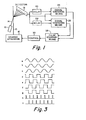
- Figure 1 is a schematic illustration showing certain equipment and circuitry for use in monitoring and controlling the diameter of an optical fibre during the drawing thereof.
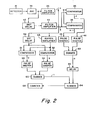
- Figure 2 is a block diagram illustration of a preferred embodiment of the present invention.
- Figure 3 is a diagram illustrating the signals appearing at various points in the circuit of Figure 2.
- Figure 1 shows a system for monitoring and controlling the diameter of an
optical fibre 10. This system includes asource 12 for providing abeam 14 of coherent, monochromatic radiation, for example a laser beam. As thefibre 10 advances axially under the influence of afibre drawing apparatus 16, thebeam 14 is directed radially on to the fibre. Adetector 18, which may comprise a scanned diode array, is suitably positioned to sense the presence of interference fringes in a predetermined range of forward scattering angles across thefibre 10 from thesource 12. - The detector signal is connected to signal comparing means 24 and 26 and is also connected to the
comparing means 24 via adelay circuit 20 and to thecomparing means 26 via adelay circuit 22. Each of the comparing means 24 and 26 produces a pulse for each peak and a pulse for each valley of the fringe pattern, the pulses from one comparing means being out of phase with respect to the pulses from the other comparing means. The combined function of signal comparing means 24 and 26 is, in effect, to provide one output pulse for each 90° portion of the fringe pattern. - The outputs from the signal comparing means are combined and counted by a pulse counting means 28 in order to generate a succession of counts representative of the diameters of successive axial portions of the advancing
fibre 10. The successive counts may be subjected to a validation process such as that described in U.S. Patent No. 4,046,536. The valid diameter indications are provided to acontrol circuit 30 where they are compared with a set point. Thecontrol circuit 30 controls the fibre drawing operation by regulating a parameter thereof such as the speed of thedrawing apparatus 16 in such a manner as to tend to reduce the variation from the set point level. - The system for processing the output from the
detector 18 is shown in greater detail in Figure 2. The locations of the signals represented as a to i in Figure 3 are indicated in Figure 2 by the letters a to i. - The total number of fringes that are contained in a given angular field are images by optics (not shown) on to the diode array of the
detector 18. Mechanical means may be employed to permit only that light which is within the desired angular range of interest to impinge upon the detector. - The
detector 18 may consist of a reticon camera containing a photodiode array and its associated electronics. The output of the camera is a sampled and held analog voltage. A commercially available model LC 100 reticon camera employs a diode array containing 1728 elements on 15 pm centres with an aperture of 11 mils. It is a self-scanning array with a serial output. Each silicon photodiode has an associated storage capacitor and a multiplexing switch for periodic feedout via an: integrated shift register scanning circuit. It is packaged with a quartz window protecting the photodiode. - The interference pattern is focused on to the diode array which is then scanned and read out on a common output line to provide an analog signal representing the fringe pattern. A discussion and illustration of fringe patterns appears in the aforementioned U.S. Patent No. 3,982,816.
- Variations in amplitude across the interference pattern can be such that amplitude falls off to a level where the signal comparing means cannot resolve the fringes. The analog signal from
detector 18 is therefor coupled to automaticgain control circuit 32 which maintains a fairly consistent amplitude across the entire pattern. - The fringe pattern signal is filtered by
filter amplifier 34 to provide a signal such as that represented by a in Figure 3. The AGC output is also delayed by a 180°delay circuit 40 and filtered by afilter amplifier 42 to provide the signal b illustrated in Figure 3. The Filter amplifiers are employed to smooth the box-car waveforms provided by the sample and hold circuit into a sinusoidal form, thereby eliminating clock noise, increasing the amplitude, and AC-coupling the signals to the comparator circuits. -
Comparators comparator 36, signal a is the reference voltage and signal b is the signal to be compared thereto.Comparator 38 uses signal b as the reference and signal a as the compared signal. The outputs fromcomparators - The outputs from
comparators pulse shapers summer 50. Thepulse shapers summer 50 may consist of an exclusive OR gate in which the high signals from both input terminals pass through to provide the output which is illustrated at h in Figure 3. - To obtain greater resolution, the circuit comprises a second pair of
comparators buffer amplifier 53 to one of the input terminals of each of these comparators, the other input signal to each comparator being amplified and delayed by passing signal a through 90°delay 54, the output of which is shown at c. In thecomparator 51 the amplified signal a is the reference voltage and the signal c is the signal being compared. Thecomparator 52 uses the signal c as the reference voltage and the amplified signal a as the compared signal. The output signals fromcomparators - The output signals from
comparators pulse shapers pulse shapers pulse shapers summer 60, the output of which is illustrated at i in Figure 3. The output from thesummer 60 is directly coupled to asummer 64 whereas the output from thesummer 50 is coupled to thesummer 64 by way of adelay circuit 66, which delays the pulses from thesummer 50 an amount sufficient to prevent them from overlapping pulses from thesummer 60. Thedelay circuit 66 may be adjustable so that an operator can vary the delay provided thereby while observing the output waveform from thesummer 64 and positioning the pulses from thesummer 50 at an optimal spacing between the pulses from thesummer 60. The pulses from thesummer 64 are connected to acounter 68, the output of which may be used to control the diameter of a drawn optical fibre as shown in Figure 1. - The disclosed system provides four pulses at the output of the
summer 64 for each cycle of the signal provided by thedetector 18. Since this circuit provides twice the number of pulses as the prior art systems, an increase in resolution of measurement is obtained. The disclosed system is therefore capable of controlling fibre diameter to a closer tolerance than that which can be achieved by the prior art.
Claims (5)
Priority Applications (1)
| Application Number | Priority Date | Filing Date | Title |
|---|---|---|---|
| AT80303102T ATE17783T1 (en) | 1979-09-04 | 1980-09-04 | SIGNAL PROCESSING SYSTEM. |
Applications Claiming Priority (2)
| Application Number | Priority Date | Filing Date | Title |
|---|---|---|---|
| US72011 | 1979-09-04 | ||
| US06/072,011 US4280827A (en) | 1979-09-04 | 1979-09-04 | System for measuring optical waveguide fiber diameter |
Publications (3)
| Publication Number | Publication Date |
|---|---|
| EP0024953A2 true EP0024953A2 (en) | 1981-03-11 |
| EP0024953A3 EP0024953A3 (en) | 1982-01-20 |
| EP0024953B1 EP0024953B1 (en) | 1986-01-29 |
Family
ID=22105002
Family Applications (1)
| Application Number | Title | Priority Date | Filing Date |
|---|---|---|---|
| EP80303102A Expired EP0024953B1 (en) | 1979-09-04 | 1980-09-04 | Signal processing system |
Country Status (6)
| Country | Link |
|---|---|
| US (1) | US4280827A (en) |
| EP (1) | EP0024953B1 (en) |
| JP (2) | JPS5644820A (en) |
| AT (1) | ATE17783T1 (en) |
| CA (1) | CA1132374A (en) |
| DE (1) | DE3071392D1 (en) |
Cited By (4)
| Publication number | Priority date | Publication date | Assignee | Title |
|---|---|---|---|---|
| FR2584180A2 (en) * | 1985-06-28 | 1987-01-02 | Thomson Csf | Device for measuring the centring of a cylindrical specimen in a transparent cylindrical coating |
| DE3715922A1 (en) * | 1986-05-15 | 1987-11-19 | Klaus Dipl Ing Jakob | Method and arrangement for measuring the thickness of a filamentary object |
| EP0720001A2 (en) * | 1994-12-30 | 1996-07-03 | Corning Incorporated | Method for monitoring the position of a fiber |
| CN104537414A (en) * | 2015-01-08 | 2015-04-22 | 山东师范大学 | Optical fringes automatic counting device and counting method based on optical fiber |
Families Citing this family (27)
| Publication number | Priority date | Publication date | Assignee | Title |
|---|---|---|---|---|
| IT1119599B (en) * | 1979-12-07 | 1986-03-10 | Cselt Centro Studi Lab Telecom | SPHERICAL SHAPING PROCEDURE OF OPTICAL FIBER TERMINATIONS |
| US4343637A (en) * | 1980-08-15 | 1982-08-10 | Owens-Corning Fiberglas Corporation | Method and apparatus for monitoring the diameter of fibers |
| FR2536860B1 (en) * | 1982-11-25 | 1985-06-14 | Saint Gobain Isover | METHOD AND DEVICE FOR THE ANALYSIS OF HETEROGENEITES IN A TRANSPARENT MATERIAL |
| GB2148273B (en) * | 1983-10-22 | 1986-11-05 | Standard Telephones Cables Ltd | Optical fibre fabrication by the rod-in-tube method |
| US4775400A (en) * | 1987-10-22 | 1988-10-04 | Ppg Industries, Inc. | Method of controlling glass fiber formation and control system |
| US4902327A (en) * | 1988-04-27 | 1990-02-20 | Raynet Corporation | Monitoring fiber bend loss characteristics during manufacture |
| US4877436A (en) * | 1989-03-13 | 1989-10-31 | Sheinkop Isac | Continuous viscosity monitoring of glass |
| JP2765033B2 (en) * | 1989-04-14 | 1998-06-11 | 住友電気工業株式会社 | Optical fiber drawing method |
| US5015867A (en) * | 1989-08-30 | 1991-05-14 | Ppg Industries, Inc. | Apparatus and methods for measuring the diameter of a moving elongated material |
| US5172421A (en) * | 1991-03-27 | 1992-12-15 | Hughes Aircraft Company | Automated method of classifying optical fiber flaws |
| US5283628A (en) * | 1991-12-31 | 1994-02-01 | Corning Incorporated | Method for measuring diameters of non-circular fibers |
| US5309221A (en) * | 1991-12-31 | 1994-05-03 | Corning Incorporated | Measurement of fiber diameters with high precision |
| US5314517A (en) * | 1992-12-31 | 1994-05-24 | Corning Incorporated | Method controlling the draw rate in the drawing of a glass feedstock |
| US5408308A (en) * | 1993-01-29 | 1995-04-18 | Corning Incorporated | Method for monitoring hermetically-coated fibers |
| US5443610A (en) * | 1994-01-29 | 1995-08-22 | Corning Incorporated | Apparatus for controlling fiber diameter during drawing |
| GB9722549D0 (en) * | 1997-10-24 | 1997-12-24 | Univ Southampton | Fabricating optical waveguide gratings and/or characterising optical waveguides |
| US6151336A (en) * | 1998-02-11 | 2000-11-21 | Sorrento Networks, Inc. | Time division multiplexing expansion subsystem |
| US6400478B1 (en) | 1998-04-02 | 2002-06-04 | Sorrento Networks, Inc. | Wavelength-division-multiplexed optical transmission system with expanded bidirectional transmission capacity over a single fiber |
| US6298103B1 (en) | 1998-06-16 | 2001-10-02 | Sorrento Networks Corporation | Flexible clock and data recovery module for a DWDM optical communication system with multiple clock rates |
| US6371394B1 (en) | 1998-12-23 | 2002-04-16 | Pirelli Cavi E Sistemi S.P.A. | Method for winding a fibre element having different longitudinal portions |
| ES2235956T3 (en) * | 1999-10-29 | 2005-07-16 | PIRELLI & C. S.P.A. | PROCEDURE FOR MEASURING TORSION TRANSMITTED TO AN OPTICAL FIBER AND PROCEDURE FOR TREATMENT OF AN OPTICAL FIBER USING THIS PROCEDURE. |
| US7072051B1 (en) | 2002-05-09 | 2006-07-04 | Powerscope Incorporated | Laser diffraction process and apparatus for width measurement of elongated objects |
| CN102159510B (en) | 2008-09-19 | 2014-03-05 | 普睿司曼股份公司 | Process for manufacturing microstructured optical fibre and method and system for on-line control of microstructured optical fibre |
| JP5017456B2 (en) * | 2009-04-09 | 2012-09-05 | 株式会社フジクラ | Method for measuring hole diameter of optical fiber with hole and method for manufacturing optical fiber with hole |
| US9939390B2 (en) | 2013-06-25 | 2018-04-10 | Prysmian S.P.A. | Method for detecting defects in a rod-shaped transparent object |
| EP3158284B1 (en) | 2014-06-17 | 2022-03-16 | Heraeus Quartz North America LLC | Apparatus and method for heating and measuring of transparent cylindrical articles |
| CN115093113B (en) * | 2022-06-17 | 2023-12-05 | 中国工程物理研究院激光聚变研究中心 | Diameter online monitoring system for micro-nano optical fiber drawing |
Citations (2)
| Publication number | Priority date | Publication date | Assignee | Title |
|---|---|---|---|---|
| US4043673A (en) * | 1975-04-09 | 1977-08-23 | Autech Corporation | Reticle calibrated diameter gauge |
| US4176961A (en) * | 1977-09-26 | 1979-12-04 | Western Electric Co., Inc. | Methods and apparatus for improving the resolution of measured parameters |
Family Cites Families (5)
| Publication number | Priority date | Publication date | Assignee | Title |
|---|---|---|---|---|
| JPS4311707Y1 (en) * | 1966-07-19 | 1968-05-21 | ||
| JPS49114475A (en) * | 1973-02-28 | 1974-10-31 | ||
| US3982816A (en) * | 1974-06-21 | 1976-09-28 | Western Electric Company, Inc. | Method for measuring the parameters of optical fibers |
| JPS5232380A (en) * | 1975-09-05 | 1977-03-11 | Yaskawa Electric Mfg Co Ltd | Photoelectric type revolution speed detector |
| US4046536A (en) * | 1976-08-13 | 1977-09-06 | Western Electric Company, Inc. | Monitoring and control of optical fiber diameters |
-
1979
- 1979-09-04 US US06/072,011 patent/US4280827A/en not_active Expired - Lifetime
-
1980
- 1980-07-10 CA CA355,896A patent/CA1132374A/en not_active Expired
- 1980-09-03 JP JP12220180A patent/JPS5644820A/en active Pending
- 1980-09-04 AT AT80303102T patent/ATE17783T1/en active
- 1980-09-04 DE DE8080303102T patent/DE3071392D1/en not_active Expired
- 1980-09-04 EP EP80303102A patent/EP0024953B1/en not_active Expired
-
1990
- 1990-03-01 JP JP1990019503U patent/JPH0428005Y2/ja not_active Expired
Patent Citations (2)
| Publication number | Priority date | Publication date | Assignee | Title |
|---|---|---|---|---|
| US4043673A (en) * | 1975-04-09 | 1977-08-23 | Autech Corporation | Reticle calibrated diameter gauge |
| US4176961A (en) * | 1977-09-26 | 1979-12-04 | Western Electric Co., Inc. | Methods and apparatus for improving the resolution of measured parameters |
Non-Patent Citations (2)
| Title |
|---|
| IBM TECHNICAL DISCLOSURE BULLETIN Vol. 10, No. 6, November 1967, New York, US F.C. BRESLAU: "Frequency Doubler" page 723 * |
| IEEE TRANSACTIONS ON INDUSTRIAL ELECTRONICS AND CONTROL INSTRUMENTATION, Vol. IECI-25, No. 2, May 1978 New York, US D.H. SMITHGALL et al.: "An optical Fiber Diameter Measurement System, Using Forward Scattered Light", pages 108-112 * |
Cited By (6)
| Publication number | Priority date | Publication date | Assignee | Title |
|---|---|---|---|---|
| FR2584180A2 (en) * | 1985-06-28 | 1987-01-02 | Thomson Csf | Device for measuring the centring of a cylindrical specimen in a transparent cylindrical coating |
| DE3715922A1 (en) * | 1986-05-15 | 1987-11-19 | Klaus Dipl Ing Jakob | Method and arrangement for measuring the thickness of a filamentary object |
| EP0720001A2 (en) * | 1994-12-30 | 1996-07-03 | Corning Incorporated | Method for monitoring the position of a fiber |
| EP0720001A3 (en) * | 1994-12-30 | 1997-04-23 | Corning Inc | Method for monitoring the position of a fiber |
| CN104537414A (en) * | 2015-01-08 | 2015-04-22 | 山东师范大学 | Optical fringes automatic counting device and counting method based on optical fiber |
| CN104537414B (en) * | 2015-01-08 | 2017-09-12 | 山东师范大学 | Optical stripe robot scaler and method of counting based on optical fiber |
Also Published As
| Publication number | Publication date |
|---|---|
| JPH0428005Y2 (en) | 1992-07-07 |
| EP0024953B1 (en) | 1986-01-29 |
| EP0024953A3 (en) | 1982-01-20 |
| DE3071392D1 (en) | 1986-03-13 |
| JPS5644820A (en) | 1981-04-24 |
| ATE17783T1 (en) | 1986-02-15 |
| CA1132374A (en) | 1982-09-28 |
| JPH02118206U (en) | 1990-09-21 |
| US4280827A (en) | 1981-07-28 |
Similar Documents
| Publication | Publication Date | Title |
|---|---|---|
| EP0024953B1 (en) | Signal processing system | |
| AU6069586A (en) | Fibre optic sensor and method of use | |
| US4027977A (en) | Method and apparatus for determining ratio of core radius to cladding radius in clad optical fibers | |
| GB1575054A (en) | Method of and apparatus for laser-beam processing of a workpiece | |
| WO1986006845A1 (en) | Optical diffraction velocimeter | |
| JPS6288905A (en) | Noncontact diameter measuring method and device for thin wire rod, etc. | |
| US4586816A (en) | Optical fibre spot size determination apparatus | |
| US4814624A (en) | Method and apparatus for measuring the position of an object boundary | |
| JPS5459166A (en) | Visual sensibility measuring apparatus of interferometer | |
| SU1594396A1 (en) | Fiber-optic reflectometer | |
| SU557258A1 (en) | Photoelectric detection of hot rolling stock | |
| SU1350498A1 (en) | Device for measuring geometric parameters of surface | |
| RU1568683C (en) | Radiant energy meter | |
| SU1060944A1 (en) | Device for measuring dynamic deformations of shafts in stationary rotating mode | |
| SU916976A1 (en) | Device for measuring object angular position | |
| SU785644A1 (en) | Photoelectric apparatus for measuring object geometrical dimensions | |
| SU739384A1 (en) | Device for measuring atmospheric refraction | |
| JP2524357B2 (en) | Optical signal processing method for optical fiber sensor for distance measurement | |
| RU2069335C1 (en) | Method of measuring distance to damaged area of fibre-optic light guide | |
| SU1637012A1 (en) | Device for checking optical pulse duration | |
| GB2133540A (en) | Optical fibre apparatus | |
| SU887968A1 (en) | Device for measuring back scattering in light-guides | |
| RU1787839C (en) | Part wear measuring device | |
| SU1516771A1 (en) | Method of remote measuring of linear dimensions of object | |
| SU1004752A1 (en) | Photoelectric meter of rotating part displacement |
Legal Events
| Date | Code | Title | Description |
|---|---|---|---|
| PUAI | Public reference made under article 153(3) epc to a published international application that has entered the european phase |
Free format text: ORIGINAL CODE: 0009012 |
|
| AK | Designated contracting states |
Designated state(s): AT BE DE FR GB IT NL SE |
|
| PUAL | Search report despatched |
Free format text: ORIGINAL CODE: 0009013 |
|
| AK | Designated contracting states |
Designated state(s): AT BE DE FR GB IT NL SE |
|
| 17P | Request for examination filed |
Effective date: 19820625 |
|
| RAP1 | Party data changed (applicant data changed or rights of an application transferred) |
Owner name: CORNING GLASS WORKS |
|
| GRAA | (expected) grant |
Free format text: ORIGINAL CODE: 0009210 |
|
| AK | Designated contracting states |
Designated state(s): AT BE DE FR GB IT NL SE |
|
| PG25 | Lapsed in a contracting state [announced via postgrant information from national office to epo] |
Ref country code: NL Effective date: 19860129 Ref country code: BE Effective date: 19860129 Ref country code: AT Effective date: 19860129 |
|
| REF | Corresponds to: |
Ref document number: 17783 Country of ref document: AT Date of ref document: 19860215 Kind code of ref document: T |
|
| PG25 | Lapsed in a contracting state [announced via postgrant information from national office to epo] |
Ref country code: SE Effective date: 19860131 |
|
| REF | Corresponds to: |
Ref document number: 3071392 Country of ref document: DE Date of ref document: 19860313 |
|
| ITF | It: translation for a ep patent filed |
Owner name: ING. A. GIAMBROCONO & C. S.R.L. |
|
| ET | Fr: translation filed | ||
| NLV1 | Nl: lapsed or annulled due to failure to fulfill the requirements of art. 29p and 29m of the patents act | ||
| PLBE | No opposition filed within time limit |
Free format text: ORIGINAL CODE: 0009261 |
|
| STAA | Information on the status of an ep patent application or granted ep patent |
Free format text: STATUS: NO OPPOSITION FILED WITHIN TIME LIMIT |
|
| 26N | No opposition filed | ||
| ITTA | It: last paid annual fee | ||
| PGFP | Annual fee paid to national office [announced via postgrant information from national office to epo] |
Ref country code: FR Payment date: 19960910 Year of fee payment: 17 |
|
| PG25 | Lapsed in a contracting state [announced via postgrant information from national office to epo] |
Ref country code: FR Free format text: THE PATENT HAS BEEN ANNULLED BY A DECISION OF A NATIONAL AUTHORITY Effective date: 19970930 |
|
| REG | Reference to a national code |
Ref country code: FR Ref legal event code: ST |
|
| PGFP | Annual fee paid to national office [announced via postgrant information from national office to epo] |
Ref country code: GB Payment date: 19980806 Year of fee payment: 19 |
|
| PGFP | Annual fee paid to national office [announced via postgrant information from national office to epo] |
Ref country code: DE Payment date: 19980928 Year of fee payment: 19 |
|
| PG25 | Lapsed in a contracting state [announced via postgrant information from national office to epo] |
Ref country code: GB Free format text: LAPSE BECAUSE OF NON-PAYMENT OF DUE FEES Effective date: 19990904 |
|
| GBPC | Gb: european patent ceased through non-payment of renewal fee |
Effective date: 19990904 |
|
| PG25 | Lapsed in a contracting state [announced via postgrant information from national office to epo] |
Ref country code: DE Free format text: LAPSE BECAUSE OF NON-PAYMENT OF DUE FEES Effective date: 20000701 |