EP0024735A2 - Nonvolatile semiconductor memory device - Google Patents
Nonvolatile semiconductor memory device Download PDFInfo
- Publication number
- EP0024735A2 EP0024735A2 EP80105168A EP80105168A EP0024735A2 EP 0024735 A2 EP0024735 A2 EP 0024735A2 EP 80105168 A EP80105168 A EP 80105168A EP 80105168 A EP80105168 A EP 80105168A EP 0024735 A2 EP0024735 A2 EP 0024735A2
- Authority
- EP
- European Patent Office
- Prior art keywords
- gate electrode
- drain
- regions
- source
- floating gate
- Prior art date
- Legal status (The legal status is an assumption and is not a legal conclusion. Google has not performed a legal analysis and makes no representation as to the accuracy of the status listed.)
- Granted
Links
- 239000004065 semiconductor Substances 0.000 title claims abstract description 26
- 238000009413 insulation Methods 0.000 claims description 15
- 239000000758 substrate Substances 0.000 claims description 12
- 230000005669 field effect Effects 0.000 abstract description 3
- 229910021420 polycrystalline silicon Inorganic materials 0.000 description 7
- VYPSYNLAJGMNEJ-UHFFFAOYSA-N Silicium dioxide Chemical compound O=[Si]=O VYPSYNLAJGMNEJ-UHFFFAOYSA-N 0.000 description 4
- 238000009792 diffusion process Methods 0.000 description 4
- 238000000034 method Methods 0.000 description 4
- 235000012239 silicon dioxide Nutrition 0.000 description 2
- 239000000377 silicon dioxide Substances 0.000 description 2
- XUIMIQQOPSSXEZ-UHFFFAOYSA-N Silicon Chemical compound [Si] XUIMIQQOPSSXEZ-UHFFFAOYSA-N 0.000 description 1
- 238000010276 construction Methods 0.000 description 1
- 230000003247 decreasing effect Effects 0.000 description 1
- 238000007599 discharging Methods 0.000 description 1
- 230000000694 effects Effects 0.000 description 1
- 229910052710 silicon Inorganic materials 0.000 description 1
- 239000010703 silicon Substances 0.000 description 1
Images
Classifications
-
- H—ELECTRICITY
- H01—ELECTRIC ELEMENTS
- H01L—SEMICONDUCTOR DEVICES NOT COVERED BY CLASS H10
- H01L29/00—Semiconductor devices adapted for rectifying, amplifying, oscillating or switching, or capacitors or resistors with at least one potential-jump barrier or surface barrier, e.g. PN junction depletion layer or carrier concentration layer; Details of semiconductor bodies or of electrodes thereof ; Multistep manufacturing processes therefor
- H01L29/66—Types of semiconductor device ; Multistep manufacturing processes therefor
- H01L29/68—Types of semiconductor device ; Multistep manufacturing processes therefor controllable by only the electric current supplied, or only the electric potential applied, to an electrode which does not carry the current to be rectified, amplified or switched
- H01L29/76—Unipolar devices, e.g. field effect transistors
- H01L29/772—Field effect transistors
- H01L29/78—Field effect transistors with field effect produced by an insulated gate
- H01L29/788—Field effect transistors with field effect produced by an insulated gate with floating gate
- H01L29/7881—Programmable transistors with only two possible levels of programmation
Definitions
- This invention relates to a nonvolatile semiconductor memory device using insulated-gate field effect transistors with both control and floating gate electrodes.
- a nonvolatile semiconductor memory device is formed by using insulated-gate field effect transistors (hereinafter referred to as IGFET's).
- IGFET's insulated-gate field effect transistors
- charging and discharging on column lines connected with memory cells or IGFET's need to be accelerated in order to increase the speed of writing and reading of data.
- the amouont of current flowing through the channel of each IGFET needs to be increased.
- This amount of current is determined by a potential of the floating gate electrode which is a substantial gate electrode of the memory cell.
- the potential of the floating gate electrode at the time of impression of a potential to the control gate electrode is determined by ratio of capacity created between the floating gate and control gate electrodes and capacity created between the floating gate electrode and the substrate inclusive of the channel.
- One method for raising the potential of the floating gate electrode to increase the amount of current is that the capacity created between the control gate electrode and floating gate electrode must be greater than the capacity created between the floating gate electrode and semiconductor substrate inclusive of the channel.
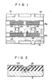
- Fig. I is a cutaway view of a semiconductor memory device developed to fulfill the aforementioned requirements, showing four memory cells.
- N +- type diffusion layers lla and llb to serve severally as source regions are formed substantially in parallel with each other in the row direction on the major surface of a P-type semiconductor substrate 10.
- N +- type diffusion layers 12a and 12b to serve as common drain regions extend between the source regions lla and llb at a given distance from each other to form a channel therebetween.
- Drain contact holes 13a and 13b are formed in the middle of the drain regions 12a and 12b, respectively.
- Polycrystalline silicon layers 14a and 14b to serve as floating gate electrodes are formed on a gate insulation film overlying two channel portions between the source region lla and the drain regions 12a and 12b, while a polycrystalline silicon layer 15a to serve as a control gate electrode is formed on another gate insulation film overlying the floating gate electrodes 14a and 14b.
- floating gate electrodes 14c and 14d and a control gate electrode 15b are successively formed on gate insulation films overlying two channel portions between the other source region llb and the drain regions 12a and 12b.
- an IGFET 16 is formed between the source region Ilb and the drain region 12b, as indicated by a chain line in Fig. 1, for example.
- Fig. 2 is a sectional view of the IGFET 16 taken along the channel portion in the row direction.
- the IGFET 16 is so designed that portions thereof other than that portion which corresponds to the channel with width W may extend on both sides of the channel in the row direction along the control gate electrode 15b.
- the distance between the IGFET 16 and an IGFET 17 adjacent thereto is increased, as shown in Fig. 1, and the dimensions b x c of the IGFET 16 become 23.0 pm x 13.5 ⁇ m, for example.
- the row-direction dimension b is expressly to large, so that the chip size of the memory 5 device will be increased in the row direction.
- the object of this invention is to provide a nonvolatile semiconductor memory device capable of high-speed writing and reading operations without increasing the chip size.
- the above object may be attained by a nonvoltage semiconductor memory device in which the width of the facing portions of a floating gate electrode and a control gate electrode along the longitudinal direction of a channel between source and drain regions of each IGFET forming a memory cell is narrower at those portions which are located over the channel than at those portions which are not located over the channel.
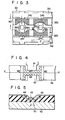
- N +- type diffusion layers 31a and 31b to serve severally as source regions are formed substantially in parallel with each other in the row direction on the major surface of a P-type semiconductor substrate 30.
- N +- type diffusion layers 32a and 32b to serve as common drain regions extend between the source regions 31a and 31b at a given distance from each other to form channels therebetween.
- Drain contact holes 33a and 33b are formed substantially in the middle of the drain regions 32a and 32b, respectively.
- Polycrystalline silicon layers 34a and 34b (reticulated portions) to serve as floating gate electrodes are formed on a gate insulation film overlying two channel portions between the source region 31a and the drain regions 32a and 32b, while a polycrystalline silicon layer 35a to serve as a control gate electrode is formed on another gate insulation film overlying the floating gate electrodes 34a and 34b. Those side edges of the control gate electrode 35a and another control gate electrode 35b which face respectively the source regions 31a and 31b extend in a straight line.
- control gate electrode 35a and the floating gate electrodes 34a and 34b are so designed that their width Wl along the longitudinal direction of the channels between the source region 31a and the drain regions 32a and 32b at those portions which are located over the channels in narrower than the width W2 at those portions which are not located over the channels. Accordingly, those side edges of the floating gate electrodes 34a and 34b and the control gate electrode 35a which face the drain contact holes 33a and 33b overlap each other, and the portions of these electrodes which are not located over the channels protrude toward the other control gate electrode 35b.
- the floating gate electrodes 34c and 34d (reticulated portions) and the control gate electrode 35b of the same configuration as aforesaid are successively formed on gate insulation films overling two channel portions between the other source region 31b and the drain regions 32a and 32b.
- four IGFET's are formed between the source regions 31a and 31b and the common'drain regions 32a and 32b.
- an IGFET 36 formed between the source region 31b and the drain region 32b is enclosed with a chain line in Fig. 3.
- the row-and column-direction dimensions d and e of the IGFET 36 are 18.5 ⁇ m and 13.5 ⁇ m, respectively. Since the row-direction dimension b of the memory cell in the prior art memory device shown in Fig.
- the area of the IGFET 36 according to this invention is smaller than that of the IGFET 16 of Fig. 1 by approximately 20 %.
- the intervals between the row lines that is, the intervals between the gate electrodes 35a and 35b and the drain contact holes 33a and 33b need to be kept larger than a given distance. This is inevitable for preventing a process error such as a possible deviation from the proper mask alignment during a photo engraving process (PEP).
- the control gate electrodes 35a and 35b jut out into a vacant space between the drain contact holes 33a and 33b, so that the memory cells are subject to no functional problems.
- the row-direction dimension of each memory cell becomes smaller than that of the conventional one to provide a high-density nonvoltile semiconductor memory device, although the facing area between the floating gate electrode and control gate electrode, that is, the value of capacity formed therebetween is the same as that of the conventional one.
- Figs. 4 and 5 show another embodiment of the nonvolatile semiconductor memory device of this invention.
- N +- type regions 41 and 42 are formed at a given distance from each other on the major surface of a P-type silicon substrate 40, serving respectively as a drain region and a source region.
- a floating gate electrode 44 extending in the widthwise direction (row direction) of a channel formed between the source and drain regions 41 and 42, is formed on a gate insulation film 43 formed of e.g. silicon dioxide overlying the channel.
- the floating gate electrode 44 is formed of e.g.
- a control gate electrode 46 is formed on a gate insulation film 45 formed of e.g. silicon dioxide overlying the floating gate electrode 44 of such configuration.
- the control gate electrode 46 is formed of e.g. polycrystalline silicon, and is so designed that a portion thereof facing the floating gate electrode 44 is of substantially the same configuration as the electrode 44, extending with the width W2 in the row direction.
- the configulation of the memory cell shown in Fig. 4. has a sufficient allowance for a possible deviation from the proper mask alignment during the PEP comparing with that shown in Fig. 1.
- a polycrystalline silicon layer used as both the control gate and floating gate electrodes deviates in the direction of lower port of Fig. 1, i.e., the control gate electrode 15b and the floating gate electrode 14d deviate in the direction of the source region llb in which the control gate electrode 15b and the floating gate electrode 14d overlap with the source region llb
- the capacity created between the floating gate electrode 14d and the substrate inclusive of the channel increases.
- the potential of the floating gate electrode is lowered.
- the channel width changes partly.
- the size of the memory cells in the row direction can be made small as described in the following order, Fig. 1 > Fig. 3 > Fig. 4 in case the capacity between the floating gate electrode and the control gate electrode in each of the memory cells in Figs. 1, 3 and 4 is the same. Accordingly, the allowance for the possible deviation from the proper mask alignment during the PEP of the memory cell of Fig. 4 is larger than those shown in Figs. 1 and 3, and that shown in Fig. 3 is larger than that shown in Fig. 1.
- the facing area between the floating gate electrode and control gate electrode is taken into account for the increase of the capacity between these gate electrodes. It is to be understood, however, that the capacity can generally be changed according to the distance between two facing electrodes and the dielectric constant of a dielectric interposed between the electrodes, besides the facing area therebetween, and that such changing methods may additionally be applied to the above embodiment.
Abstract
Description
- This invention relates to a nonvolatile semiconductor memory device using insulated-gate field effect transistors with both control and floating gate electrodes.
- A nonvolatile semiconductor memory device is formed by using insulated-gate field effect transistors (hereinafter referred to as IGFET's). In this semiconductor memory device, charging and discharging on column lines connected with memory cells or IGFET's need to be accelerated in order to increase the speed of writing and reading of data. To attain this, the amouont of current flowing through the channel of each IGFET needs to be increased. This amount of current is determined by a potential of the floating gate electrode which is a substantial gate electrode of the memory cell. The potential of the floating gate electrode at the time of impression of a potential to the control gate electrode is determined by ratio of capacity created between the floating gate and control gate electrodes and capacity created between the floating gate electrode and the substrate inclusive of the channel. One method for raising the potential of the floating gate electrode to increase the amount of current is that the capacity created between the control gate electrode and floating gate electrode must be greater than the capacity created between the floating gate electrode and semiconductor substrate inclusive of the channel.
- Fig. I is a cutaway view of a semiconductor memory device developed to fulfill the aforementioned requirements, showing four memory cells. In Fig. 1, N+-type diffusion layers lla and llb to serve severally as source regions are formed substantially in parallel with each other in the row direction on the major surface of a P-
type semiconductor substrate 10. N+-type diffusion layers 12a and 12b to serve as common drain regions extend between the source regions lla and llb at a given distance from each other to form a channel therebetween. Draincontact holes 13a and 13b are formed in the middle of the drain regions 12a and 12b, respectively.Polycrystalline silicon layers 14a and 14b to serve as floating gate electrodes are formed on a gate insulation film overlying two channel portions between the source region lla and the drain regions 12a and 12b, while a polycrystalline silicon layer 15a to serve as a control gate electrode is formed on another gate insulation film overlying the floatinggate electrodes 14a and 14b. Likewise, floatinggate electrodes 14c and 14d and acontrol gate electrode 15b are successively formed on gate insulation films overlying two channel portions between the other source region llb and the drain regions 12a and 12b. Thus, anIGFET 16 is formed between the source region Ilb and the drain region 12b, as indicated by a chain line in Fig. 1, for example. - Fig. 2 is a sectional view of the
IGFET 16 taken along the channel portion in the row direction. In order to increase the capacity between thecontrol gate electroe 15b and thefloating gate electrode 14d, the IGFET 16 is so designed that portions thereof other than that portion which corresponds to the channel with width W may extend on both sides of the channel in the row direction along thecontrol gate electrode 15b. As a result, the distance between theIGFET 16 and anIGFET 17 adjacent thereto is increased, as shown in Fig. 1, and the dimensions b x c of the IGFET 16 become 23.0 pm x 13.5 µm, for example. Thus, the row-direction dimension b is expressly to large, so that the chip size of the memory 5 device will be increased in the row direction. - Acordingly, the object of this invention is to provide a nonvolatile semiconductor memory device capable of high-speed writing and reading operations without increasing the chip size.
- According to this invention, the above object may be attained by a nonvoltage semiconductor memory device in which the width of the facing portions of a floating gate electrode and a control gate electrode along the longitudinal direction of a channel between source and drain regions of each IGFET forming a memory cell is narrower at those portions which are located over the channel than at those portions which are not located over the channel.
- This invention can be more fully understood from the following detailed description when taken in conjunction with the accompanying drawings, in which:
- Fig. 1 is a cutaway plan view of a prior art nonvolatile semiconductor memory device;
- Fig. 2 is a sectional view of one memory cell shown in Fig. 1 taken along its channel portion;
- Fig. 3 is a cutaway plan view of a nonvolatile semiconductor memory device according to an embodiment of this invention;
- Fig. 4 is a plan view of a nonvolatile semiconductor memory device according to another embodiment of the invention; and
- Fig. 5 is a sectional view of a memory cell shown in Fig. 4 taken along its channel portion.
- In Fig. 3, N+-type diffusion layers 31a and 31b to serve severally as source regions are formed substantially in parallel with each other in the row direction on the major surface of a P-
type semiconductor substrate 30. N+-type diffusion layers 32a and 32b to serve as common drain regions extend between the source regions 31a and 31b at a given distance from each other to form channels therebetween.Drain contact holes 33a and 33b are formed substantially in the middle of the drain regions 32a and 32b, respectively.Polycrystalline silicon layers polycrystalline silicon layer 35a to serve as a control gate electrode is formed on another gate insulation film overlying thefloating gate electrodes control gate electrode 35a and anothercontrol gate electrode 35b which face respectively the source regions 31a and 31b extend in a straight line. Thecontrol gate electrode 35a and thefloating gate electrodes floating gate electrodes control gate electrode 35a which face thedrain contact holes 33a and 33b overlap each other, and the portions of these electrodes which are not located over the channels protrude toward the othercontrol gate electrode 35b. - Likewise, the
floating gate electrodes 34c and 34d (reticulated portions) and thecontrol gate electrode 35b of the same configuration as aforesaid are successively formed on gate insulation films overling two channel portions between the other source region 31b and the drain regions 32a and 32b. Thus, four IGFET's are formed between the source regions 31a and 31b and the common'drain regions 32a and 32b. For example, an IGFET 36 formed between the source region 31b and the drain region 32b is enclosed with a chain line in Fig. 3. Here the row-and column-direction dimensions d and e of theIGFET 36 are 18.5 µm and 13.5 µm, respectively. Since the row-direction dimension b of the memory cell in the prior art memory device shown in Fig. I is b = 23.0 µm, the area of the IGFET 36 according to this invention is smaller than that of the IGFET 16 of Fig. 1 by approximately 20 %. Generally, in an integrated circuit such as a nonvolatile semiconductor memory device using IGFET's as its memory cells as has been described in this specification, the intervals between the row lines, that is, the intervals between thegate electrodes drain contact holes 33a and 33b need to be kept larger than a given distance. This is inevitable for preventing a process error such as a possible deviation from the proper mask alignment during a photo engraving process (PEP). According to the embodiment of Fig, 3, however, thecontrol gate electrodes drain contact holes 33a and 33b, so that the memory cells are subject to no functional problems. - With such construction of the IGFET's to serve as memory cells, the row-direction dimension of each memory cell becomes smaller than that of the conventional one to provide a high-density nonvoltile semiconductor memory device, although the facing area between the floating gate electrode and control gate electrode, that is, the value of capacity formed therebetween is the same as that of the conventional one.
- Figs. 4 and 5 show another embodiment of the nonvolatile semiconductor memory device of this invention. In Figs. 4 and 5, N+-type regions 41 and 42 are formed at a given distance from each other on the major surface of a P-
type silicon substrate 40, serving respectively as a drain region and a source region. Afloating gate electrode 44, extending in the widthwise direction (row direction) of a channel formed between the source anddrain regions 41 and 42, is formed on agate insulation film 43 formed of e.g. silicon dioxide overlying the channel. Thefloating gate electrode 44 is formed of e.g. polycrystalline silicon, and is so designed that a portion of theelectrode 44 on thegate insulation film 43 corresponding to the channel has a smaller width Wl and those portions which are not located over the channel have a greater width W2. Acontrol gate electrode 46 is formed on agate insulation film 45 formed of e.g. silicon dioxide overlying thefloating gate electrode 44 of such configuration. Thecontrol gate electrode 46 is formed of e.g. polycrystalline silicon, and is so designed that a portion thereof facing thefloating gate electrode 44 is of substantially the same configuration as theelectrode 44, extending with the width W2 in the row direction. - Also in the case of the embodiment shown in Figs. 4 and 5, even if the facing area between the
floating gate electrode 44 andcontrol gate electrode 46 that is, the capacity between these electrodes is the same as that of the conventional one, the row-direction dimension of the memory cell can be reduced. - The configulation of the memory cell shown in Fig. 4. has a sufficient allowance for a possible deviation from the proper mask alignment during the PEP comparing with that shown in Fig. 1. For example, if a polycrystalline silicon layer used as both the control gate and floating gate electrodes deviates in the direction of lower port of Fig. 1, i.e., the
control gate electrode 15b and thefloating gate electrode 14d deviate in the direction of the source region llb in which thecontrol gate electrode 15b and thefloating gate electrode 14d overlap with the source region llb, the capacity created between thefloating gate electrode 14d and the substrate inclusive of the channel increases. As a result the potential of the floating gate electrode is lowered. Also, the channel width changes partly. - On the other hand, according to the configulation of the memory cell shown in Fig. 4, even if the deviation occurs by the similar extent as in the configulation shown in Fig. 1, the overlapping area of the source region and the floating gate electrode scarcely increases, the capacity created between the floating gate electrode and the substrate inclusive of the channel scarcely increases and the potential of the floating gate electrode is scarcely lowered. Also no undesirable effect is applied on the channel region. The reason of this that the size of the memory cell of Fig. 4 is decreased in the row direction thereof, though size in the column direction is increased.
- When compared the memory cells shown in Figs. 1, 3 and 4, the size of the memory cells in the row direction can be made small as described in the following order, Fig. 1 > Fig. 3 > Fig. 4 in case the capacity between the floating gate electrode and the control gate electrode in each of the memory cells in Figs. 1, 3 and 4 is the same. Accordingly, the allowance for the possible deviation from the proper mask alignment during the PEP of the memory cell of Fig. 4 is larger than those shown in Figs. 1 and 3, and that shown in Fig. 3 is larger than that shown in Fig. 1.
- In the above-mentioned embodiment, only the facing area between the floating gate electrode and control gate electrode is taken into account for the increase of the capacity between these gate electrodes. It is to be understood, however, that the capacity can generally be changed according to the distance between two facing electrodes and the dielectric constant of a dielectric interposed between the electrodes, besides the facing area therebetween, and that such changing methods may additionally be applied to the above embodiment.
Claims (4)
characterized in that the width of said floating gate electrode (34a-34d, 44) and control gate electrode (35a, 35b, 46) along the longitudinal direction of the channel between said source (31a, 31b, 41) and drain (32a, 32b, 42) regions is narrower at those portions (Wl) which are located over said channel than at those portions (W2) which are not located over said channel.
characterized in that first and second source regions (31a, 31b) are formed substantially in paralle with each other in the row direction on the major surface of the semiconductor substrate (30), a common drain region (32a) is extended between the first and second source regions (31a, 31b) to form channels therebetween, a drain contact hole (33a) is formed substantially in the middle of the drain region (32a), first and second floating gate electrodes (34a, 34c) are formed on one gate insulation film overlying said channels, first and second control gate electrodes (35a, 35b) are formed on another gate insulation film overlying the first and second floating gate electrodes (34a, 34c) in such a manner that those side edges of the first and second floating and control gate electrodes (34a, 34c, 35a, 35b) which face the first and second source regions (31a, 31b) are substantially in line with each other and extend in a substantial straight line, and those side edges of the first and second floating and control gate electrodes (34a, 34c, 35a, 35b) which face said drain contact hole (33a) have portions not located over the channels protruding in the longitudinal direction of the channels, whereby the width of said floating gate electrodes (34a, 34c) and control gate electrodes (35a, 35b) along the longitudinal direction of the channels between said source (31a, 31b) and drain (32a) regions is narrower at those portions (Wl) which are located over said channels than at those portions (W2) which are not located over said channels.
Applications Claiming Priority (2)
| Application Number | Priority Date | Filing Date | Title |
|---|---|---|---|
| JP111111/79 | 1979-08-31 | ||
| JP11111179A JPS5636166A (en) | 1979-08-31 | 1979-08-31 | Nonvolatile semiconductor memory |
Publications (3)
| Publication Number | Publication Date |
|---|---|
| EP0024735A2 true EP0024735A2 (en) | 1981-03-11 |
| EP0024735A3 EP0024735A3 (en) | 1981-08-26 |
| EP0024735B1 EP0024735B1 (en) | 1985-01-16 |
Family
ID=14552681
Family Applications (1)
| Application Number | Title | Priority Date | Filing Date |
|---|---|---|---|
| EP80105168A Expired EP0024735B1 (en) | 1979-08-31 | 1980-08-29 | Nonvolatile semiconductor memory device |
Country Status (4)
| Country | Link |
|---|---|
| US (1) | US4395724A (en) |
| EP (1) | EP0024735B1 (en) |
| JP (1) | JPS5636166A (en) |
| DE (1) | DE3069974D1 (en) |
Cited By (2)
| Publication number | Priority date | Publication date | Assignee | Title |
|---|---|---|---|---|
| FR2638285A1 (en) * | 1988-10-25 | 1990-04-27 | Commissariat Energie Atomique | HIGH-DENSITY INTEGRATED INTEGRATED CIRCUIT SUCH AS MEMORY EPROM AND CORRESPONDING OBTAINING METHOD |
| EP0414412A2 (en) * | 1989-08-22 | 1991-02-27 | Hitachi, Ltd. | Semiconductor integrated circuit device having wiring layers |
Families Citing this family (5)
| Publication number | Priority date | Publication date | Assignee | Title |
|---|---|---|---|---|
| US4577215A (en) * | 1983-02-18 | 1986-03-18 | Rca Corporation | Dual word line, electrically alterable, nonvolatile floating gate memory device |
| JPH0677440A (en) * | 1992-08-27 | 1994-03-18 | Mitsubishi Electric Corp | Nonvolatile semiconductor memory |
| JP2848211B2 (en) * | 1993-10-08 | 1999-01-20 | 日本電気株式会社 | Nonvolatile semiconductor memory device |
| US5780894A (en) * | 1996-02-23 | 1998-07-14 | Nippon Steel Corporation | Nonvolatile semiconductor memory device having stacked-gate type transistor |
| DE19929619C2 (en) * | 1999-06-28 | 2001-06-28 | Infineon Technologies Ag | Semiconductor memory cell pair |
Citations (4)
| Publication number | Priority date | Publication date | Assignee | Title |
|---|---|---|---|---|
| FR1408613A (en) * | 1963-09-25 | 1965-08-13 | Philips Nv | Method for applying two neighboring surface layers on a support, preferably for the manufacture of a semiconductor device |
| US3825945A (en) * | 1972-02-29 | 1974-07-23 | Tokyo Shibaura Electric Co | Field effect semiconductor memory apparatus with a floating gate |
| US4161039A (en) * | 1976-12-15 | 1979-07-10 | Siemens Aktiengesellschaft | N-Channel storage FET |
| JPS5493375A (en) * | 1977-12-30 | 1979-07-24 | Fujitsu Ltd | Semiconductor integrated circuit device |
Family Cites Families (3)
| Publication number | Priority date | Publication date | Assignee | Title |
|---|---|---|---|---|
| US4099196A (en) * | 1977-06-29 | 1978-07-04 | Intel Corporation | Triple layer polysilicon cell |
| US4203158A (en) * | 1978-02-24 | 1980-05-13 | Intel Corporation | Electrically programmable and erasable MOS floating gate memory device employing tunneling and method of fabricating same |
| JPS55166964A (en) * | 1979-06-14 | 1980-12-26 | Mitsubishi Electric Corp | Avalanche injection type non-volatile semiconductor memory |
-
1979
- 1979-08-31 JP JP11111179A patent/JPS5636166A/en active Granted
-
1980
- 1980-08-22 US US06/180,435 patent/US4395724A/en not_active Expired - Lifetime
- 1980-08-29 EP EP80105168A patent/EP0024735B1/en not_active Expired
- 1980-08-29 DE DE8080105168T patent/DE3069974D1/en not_active Expired
Patent Citations (4)
| Publication number | Priority date | Publication date | Assignee | Title |
|---|---|---|---|---|
| FR1408613A (en) * | 1963-09-25 | 1965-08-13 | Philips Nv | Method for applying two neighboring surface layers on a support, preferably for the manufacture of a semiconductor device |
| US3825945A (en) * | 1972-02-29 | 1974-07-23 | Tokyo Shibaura Electric Co | Field effect semiconductor memory apparatus with a floating gate |
| US4161039A (en) * | 1976-12-15 | 1979-07-10 | Siemens Aktiengesellschaft | N-Channel storage FET |
| JPS5493375A (en) * | 1977-12-30 | 1979-07-24 | Fujitsu Ltd | Semiconductor integrated circuit device |
Non-Patent Citations (2)
| Title |
|---|
| IEEE Trans. Elect. Devices Vol. ED-24, No. 5, May 1977 pp. 600-610 * |
| Patent Abstracts of Japan, Vol. 3, p. 125E140 * |
Cited By (4)
| Publication number | Priority date | Publication date | Assignee | Title |
|---|---|---|---|---|
| FR2638285A1 (en) * | 1988-10-25 | 1990-04-27 | Commissariat Energie Atomique | HIGH-DENSITY INTEGRATED INTEGRATED CIRCUIT SUCH AS MEMORY EPROM AND CORRESPONDING OBTAINING METHOD |
| EP0369842A1 (en) * | 1988-10-25 | 1990-05-23 | Commissariat A L'energie Atomique | Method for the production of a large-scale integrated circuit such as an EPROM |
| EP0414412A2 (en) * | 1989-08-22 | 1991-02-27 | Hitachi, Ltd. | Semiconductor integrated circuit device having wiring layers |
| EP0414412A3 (en) * | 1989-08-22 | 1991-11-21 | Hitachi, Ltd. | Semiconductor integrated circuit device having wiring layers |
Also Published As
| Publication number | Publication date |
|---|---|
| JPS6244702B2 (en) | 1987-09-22 |
| DE3069974D1 (en) | 1985-02-28 |
| JPS5636166A (en) | 1981-04-09 |
| EP0024735B1 (en) | 1985-01-16 |
| EP0024735A3 (en) | 1981-08-26 |
| US4395724A (en) | 1983-07-26 |
Similar Documents
| Publication | Publication Date | Title |
|---|---|---|
| US4355375A (en) | Semiconductor memory device | |
| EP0135824B1 (en) | Semiconductor memory device | |
| US5877537A (en) | Semiconductor device having first transistor rows with second transistor rows connected therebetween | |
| US4663644A (en) | Semiconductor device and method of manufacturing the same | |
| US6579762B2 (en) | Nonvolatile semiconductor device having a memory cells each of which is constituted of a memory transistor and a selection transistor | |
| US6128209A (en) | Semiconductor memory device having dummy bit and word lines | |
| US20230299182A1 (en) | Semiconductor device and method of forming the same | |
| US4967393A (en) | Flash erasable and programmable nonvolatile semiconductor memory | |
| US4737835A (en) | Read only memory semiconductor device | |
| KR100201451B1 (en) | Nonvolatile memory device | |
| EP0024735A2 (en) | Nonvolatile semiconductor memory device | |
| US3760384A (en) | Fet memory chip including fet devices therefor and fabrication method | |
| US4831425A (en) | Integrated circuit having improved contact region | |
| EP0432792B1 (en) | Nonvolatile semiconductor memory device and method of manufacturing the same | |
| KR950014540B1 (en) | Process for forming arrayed field effect transistors highly integrated on substrate | |
| US5880499A (en) | Memory cell of a nonvolatile semiconductor device | |
| KR0169510B1 (en) | Nonvolatile semiconductor memory and fabrication thereof | |
| US6017793A (en) | Method of forming a memory cell of a nonvolatile semiconductor memory device | |
| KR19980055726A (en) | Flash memory device and program, erase and read method using same | |
| JPS605062B2 (en) | semiconductor logic circuit device | |
| JPH03225965A (en) | Nonvolatile semiconductor memory device of ultraviolet erasure type | |
| US6071778A (en) | Memory device with a memory cell array in triple well, and related manufacturing process | |
| US5966325A (en) | Semiconductor memory device with improved read speed | |
| US6288942B1 (en) | Nonvolatile semiconductor storage device and its manufacturing method | |
| KR100248686B1 (en) | Non-volatile semiconductor memory with floating gate and control gate and fabrication process therefor |
Legal Events
| Date | Code | Title | Description |
|---|---|---|---|
| PUAI | Public reference made under article 153(3) epc to a published international application that has entered the european phase |
Free format text: ORIGINAL CODE: 0009012 |
|
| 17P | Request for examination filed |
Effective date: 19800829 |
|
| AK | Designated contracting states |
Designated state(s): DE FR GB |
|
| PUAL | Search report despatched |
Free format text: ORIGINAL CODE: 0009013 |
|
| AK | Designated contracting states |
Designated state(s): DE FR GB |
|
| RAP1 | Party data changed (applicant data changed or rights of an application transferred) |
Owner name: KABUSHIKI KAISHA TOSHIBA |
|
| GRAA | (expected) grant |
Free format text: ORIGINAL CODE: 0009210 |
|
| AK | Designated contracting states |
Designated state(s): DE FR GB |
|
| REF | Corresponds to: |
Ref document number: 3069974 Country of ref document: DE Date of ref document: 19850228 |
|
| ET | Fr: translation filed | ||
| PLBE | No opposition filed within time limit |
Free format text: ORIGINAL CODE: 0009261 |
|
| STAA | Information on the status of an ep patent application or granted ep patent |
Free format text: STATUS: NO OPPOSITION FILED WITHIN TIME LIMIT |
|
| 26N | No opposition filed | ||
| REG | Reference to a national code |
Ref country code: GB Ref legal event code: 746 |
|
| PGFP | Annual fee paid to national office [announced via postgrant information from national office to epo] |
Ref country code: FR Payment date: 19990810 Year of fee payment: 20 |
|
| PGFP | Annual fee paid to national office [announced via postgrant information from national office to epo] |
Ref country code: GB Payment date: 19990825 Year of fee payment: 20 |
|
| PGFP | Annual fee paid to national office [announced via postgrant information from national office to epo] |
Ref country code: DE Payment date: 19990827 Year of fee payment: 20 |
|
| REG | Reference to a national code |
Ref country code: FR Ref legal event code: D6 |
|
| PG25 | Lapsed in a contracting state [announced via postgrant information from national office to epo] |
Ref country code: GB Free format text: LAPSE BECAUSE OF EXPIRATION OF PROTECTION Effective date: 20000828 |
|
| REG | Reference to a national code |
Ref country code: GB Ref legal event code: PE20 Effective date: 20000828 |