EP0022383B1 - Procédé de réalisation d'un transistor à effet de champ à grille Schottky auto-alignée, et transistor obtenu par ce procédé - Google Patents
Procédé de réalisation d'un transistor à effet de champ à grille Schottky auto-alignée, et transistor obtenu par ce procédé Download PDFInfo
- Publication number
- EP0022383B1 EP0022383B1 EP80400816A EP80400816A EP0022383B1 EP 0022383 B1 EP0022383 B1 EP 0022383B1 EP 80400816 A EP80400816 A EP 80400816A EP 80400816 A EP80400816 A EP 80400816A EP 0022383 B1 EP0022383 B1 EP 0022383B1
- Authority
- EP
- European Patent Office
- Prior art keywords
- layer
- grid
- transistor
- source
- isolating
- Prior art date
- Legal status (The legal status is an assumption and is not a legal conclusion. Google has not performed a legal analysis and makes no representation as to the accuracy of the status listed.)
- Expired
Links
Images


Classifications
-
- H—ELECTRICITY
- H10—SEMICONDUCTOR DEVICES; ELECTRIC SOLID-STATE DEVICES NOT OTHERWISE PROVIDED FOR
- H10D—INORGANIC ELECTRIC SEMICONDUCTOR DEVICES
- H10D30/00—Field-effect transistors [FET]
- H10D30/01—Manufacture or treatment
- H10D30/061—Manufacture or treatment of FETs having Schottky gates
- H10D30/0612—Manufacture or treatment of FETs having Schottky gates of lateral single-gate Schottky FETs
-
- H—ELECTRICITY
- H10—SEMICONDUCTOR DEVICES; ELECTRIC SOLID-STATE DEVICES NOT OTHERWISE PROVIDED FOR
- H10D—INORGANIC ELECTRIC SEMICONDUCTOR DEVICES
- H10D30/00—Field-effect transistors [FET]
- H10D30/80—FETs having rectifying junction gate electrodes
- H10D30/87—FETs having Schottky gate electrodes, e.g. metal-semiconductor FETs [MESFET]
-
- H—ELECTRICITY
- H10—SEMICONDUCTOR DEVICES; ELECTRIC SOLID-STATE DEVICES NOT OTHERWISE PROVIDED FOR
- H10D—INORGANIC ELECTRIC SEMICONDUCTOR DEVICES
- H10D64/00—Electrodes of devices having potential barriers
- H10D64/01—Manufacture or treatment
- H10D64/012—Manufacture or treatment of electrodes comprising a Schottky barrier to a semiconductor
- H10D64/0124—Manufacture or treatment of electrodes comprising a Schottky barrier to a semiconductor to Group III-V semiconductors
- H10D64/0125—Manufacture or treatment of electrodes comprising a Schottky barrier to a semiconductor to Group III-V semiconductors characterised by the sectional shape, e.g. T or inverted T
-
- H—ELECTRICITY
- H10—SEMICONDUCTOR DEVICES; ELECTRIC SOLID-STATE DEVICES NOT OTHERWISE PROVIDED FOR
- H10P—GENERIC PROCESSES OR APPARATUS FOR THE MANUFACTURE OR TREATMENT OF DEVICES COVERED BY CLASS H10
- H10P76/00—Manufacture or treatment of masks on semiconductor bodies, e.g. by lithography or photolithography
- H10P76/40—Manufacture or treatment of masks on semiconductor bodies, e.g. by lithography or photolithography of masks comprising inorganic materials
-
- Y—GENERAL TAGGING OF NEW TECHNOLOGICAL DEVELOPMENTS; GENERAL TAGGING OF CROSS-SECTIONAL TECHNOLOGIES SPANNING OVER SEVERAL SECTIONS OF THE IPC; TECHNICAL SUBJECTS COVERED BY FORMER USPC CROSS-REFERENCE ART COLLECTIONS [XRACs] AND DIGESTS
- Y10—TECHNICAL SUBJECTS COVERED BY FORMER USPC
- Y10S—TECHNICAL SUBJECTS COVERED BY FORMER USPC CROSS-REFERENCE ART COLLECTIONS [XRACs] AND DIGESTS
- Y10S148/00—Metal treatment
- Y10S148/053—Field effect transistors fets
-
- Y—GENERAL TAGGING OF NEW TECHNOLOGICAL DEVELOPMENTS; GENERAL TAGGING OF CROSS-SECTIONAL TECHNOLOGIES SPANNING OVER SEVERAL SECTIONS OF THE IPC; TECHNICAL SUBJECTS COVERED BY FORMER USPC CROSS-REFERENCE ART COLLECTIONS [XRACs] AND DIGESTS
- Y10—TECHNICAL SUBJECTS COVERED BY FORMER USPC
- Y10S—TECHNICAL SUBJECTS COVERED BY FORMER USPC CROSS-REFERENCE ART COLLECTIONS [XRACs] AND DIGESTS
- Y10S148/00—Metal treatment
- Y10S148/106—Masks, special
-
- Y—GENERAL TAGGING OF NEW TECHNOLOGICAL DEVELOPMENTS; GENERAL TAGGING OF CROSS-SECTIONAL TECHNOLOGIES SPANNING OVER SEVERAL SECTIONS OF THE IPC; TECHNICAL SUBJECTS COVERED BY FORMER USPC CROSS-REFERENCE ART COLLECTIONS [XRACs] AND DIGESTS
- Y10—TECHNICAL SUBJECTS COVERED BY FORMER USPC
- Y10S—TECHNICAL SUBJECTS COVERED BY FORMER USPC CROSS-REFERENCE ART COLLECTIONS [XRACs] AND DIGESTS
- Y10S148/00—Metal treatment
- Y10S148/139—Schottky barrier
-
- Y—GENERAL TAGGING OF NEW TECHNOLOGICAL DEVELOPMENTS; GENERAL TAGGING OF CROSS-SECTIONAL TECHNOLOGIES SPANNING OVER SEVERAL SECTIONS OF THE IPC; TECHNICAL SUBJECTS COVERED BY FORMER USPC CROSS-REFERENCE ART COLLECTIONS [XRACs] AND DIGESTS
- Y10—TECHNICAL SUBJECTS COVERED BY FORMER USPC
- Y10S—TECHNICAL SUBJECTS COVERED BY FORMER USPC CROSS-REFERENCE ART COLLECTIONS [XRACs] AND DIGESTS
- Y10S438/00—Semiconductor device manufacturing: process
- Y10S438/942—Masking
- Y10S438/948—Radiation resist
- Y10S438/951—Lift-off
Definitions
- the invention relates to methods for producing so-called field effect transistors with self-alignment of the gate with respect to the source and drain electrodes.
- a drawback common to the aforementioned methods stems from the fact that the layer of material remaining after the first masking and remaining on the transistor, even after finishing, constitutes a source of cracks and breaks in the insulating surface layer of the transistor due to the difference in thermal expansion, especially in the case of gallium arsenide transistors, particularly for high power transistors.
- the invention remedies this drawback by allowing the active layer of gallium arsenide of the field effect transistor to remain, two superposed protective layers formed one, of polycrystalline gallium arsenide, the other of gallium arsenide and aluminum.
- the method is characterized in that the first insulating or semi-insulating material is polycrystalline gallium arsenide and the second insulating material is gallium and aluminum arsenide, the order of use of the materials can be reversed.
- Figure 1 shows a fraction of a semi-insulating monocrystalline gallium arsenide substrate 1, on which a layer 2 of n-doped gallium arsenide has been grown by epitaxy, intended to act as a layer active of a field effect transistor.
- a thin layer 3 of semi-insulating polycrystalline gallium arsenide was deposited by a conventional method.
- FIG 2 there is shown the wafer of Figure 1, after treatment, covered with a mask 30 having three windows 31, 32 and 33.
- This mask was obtained by developing the resin 3 and then attacking the wafer with using an agent capable of removing the unprotected parts of the material from layer 3.
- the result obtained after removal of the remainder 40 of the resin 4 is shown.
- the attack is carried out either by ionic machining or by chemical attack using an agent to which the resin is not very sensitive, or preferably using a localized plasma etching reactor using a gas chosen according to the material to be attacked selectively.
- a layer 5 much thicker (of the order of half a micron if the layer 3 is of the order of a tenth of a micron), was deposited with a second material, which is also insulating or semi-insulating, distinguished from the first by the possibility of a selective attack.
- Gallium and aluminum arsenide will be used if the first material is pure gallium arsenide. It could be the reverse.
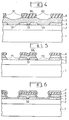
- Figure 4 there is shown the plate of Figure 3 after development of a mask 6 of resin comprising two windows located at the locations of the future source and drain, that is to the right of the windows 31 and 33 of the mask 30. It is not necessary to determine with great precision the location and size of each opening because it suffices to ensure the effective protection of the window 32 (currently filled with the second material), by the resin pin 60 constituting the central part of the mask 6. In practice, a tolerance is adopted on the dimensions leading to having windows 61 and 62 slightly wider than the windows 31 and 32.
- the resin used to produce the mask 30 may be of the photosensitive type.
- Figure 5 shows the result obtained after attacking the second material. This attack can be carried out either using selective chemical agents or a localized plasma etching reactor. It produces windows 71 and 72 exposing the material of layer 2.
- Figure 6 there is shown the wafer of Figure 5 after depositing a layer 7 obtained by evaporation under vacuum of metal on the entire wafer, the resin 6 being left as it was at the end of the previous step.
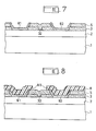
- Figure 7 shows the wafer after development with a solvent which removes the resin 6 according to the technology known in the English literature under the term "lift-off •.
- the part of the metal layer covering the resin is removed at the same time as the resin which served as its support.
- Figure 8 is shown the plate of Figure 7 after development of a mask 8 of photosensitive resin comprising a window 80 located at the location of the future grid, or to the right of the window 32 of the mask consisting of the first semi material -insulating, window currently filled with the second material.
- the dimensions of window 80 are purposely much larger than those of window 32.
- FIG 9 there is shown the plate of Figure 8 after attack of the second semi-insulating material, attack carried out in one of the ways already mentioned with respect to Figure 5.
- the result is constituted by the opening of a window 90 giving wide access to the window 32 in which the material of the layer 2 has been exposed.
- FIG. 10 shows the result obtained after depositing a layer of metal of which there remains only one pin 100 filling the window 90. This deposition was carried out by evaporation under vacuum of metal followed by an operation of "lift- off exposing the rest of the wafer, in particular the region of the contacts 81 and 82 of source and drain.
- the pin 100 makes the gate contact, of the Schottky type.
- FIG. 10 constitutes that of a field effect transistor whose passivation layer comprises two different materials. There is thus a component practically ready for use.
- the components In the case of collective manufacture of a large number of identical transistors on the same wafer (only one of them has been shown in FIGS. 1 to 10), the components must however be separated by a mechanical or chemical method or a combination of these two types of methods, in a conventional manner.
Landscapes
- Junction Field-Effect Transistors (AREA)
Description
- L'invention se rapporte aux procédés de réalisation de transistors à effet de champ dits « à auto-alignement de la grille par rapport aux électrodes de source et de drain.
- On connaît, par le document SIEMENS FORS-CHUNGS und ENTWICKLUNGS-BERICHTE, vol. 5, N° 3, mars 1976, pages 136-138, un procédé de réalisation d'un transistor à effet de champ à grille Schottky, où la position et les dimensions de la grille, ainsi que les intervalles entre source et grille, grille et drain sont fixés dès la première opération de masquage par la réalisation de fenêtres de source, de grille et de drain dans un premier matériau. On utilise un même métal (le platine) pour réaliser les contacts ohmiques et Schottky, la différenciation des contacts étant obtenue grâce à un surdopage préalable des zones semiconductrices devant recevoir les contacts ohmiques.
- Il est par ailleurs possible à l'homme de métier d'utiliser un procédé analogue à celui du document précité, en utilisant deux métaux différents, l'un formant un contact ohmique avec le matériau semiconducteur et l'autre formant un contact Schottky. Il utilisera à cet effet deux matériaux différents de masquage attaquables sélectivement par des agents de gravure différents.
- Un inconvénient commun aux procédés précité provient du fait que la couche de matériau subsistant après le premier masquage et demeurant sur le transistor, même après finition, constitue une source de fêlures et de cassures dans la couche superficielle isolante du transistor par suite de la différence de dilatation thermique, notamment dans le cas des transistors à l'arséniure de gallium, particulièrement pour les transistors de forte puissance.
- L'invention remédie à cet inconvénient en laissant subsister sur la couche active en arséniure de gallium du transistor à effet de champ, deux couches protectrices superposées formées l'une, d'arséniure de gallium polycristallin, l'autre d'arséniure de gallium et d'aluminium.
- Le procédé selon l'invention est du type comportant au moins les étapes suivantes :
- - réalisation, sur la couche semiconductrice active du transistor, d'un masque constitué par un premier matériau, isolant ou semi-isolant, comportant des fenêtres déterminant les dimensions et l'emplacement définitif de la source, de la grille et du drain du transistor à réaliser ;
- - dépôt d'une couche d'un deuxième matériau isolant, attaquable sélectivement par un agent qui n'attaque pas ou attaque à vitesse beaucoup plus faible le premier matériau ;
- - ouverture, par photogravure effectuée à l'aide dudit agent, de fenêtres de source et de drain mettant à nu le semiconducteur ;
- - dépôt des contacts ohmiques de source et de drain ;
- - ouverture, par photogravure effectuée à l'aide dudit agent, dans le deuxième matériau, d'une fenêtre dégageant la fenêtre initiale de grille plus grande que celle-ci, et mettant à nu, dans celle-ci, le semiconducteur ;
- - dépôt du contact de grille.
- Le procédé est caractérisé en ce que le premier matériau isolant ou semi-isolant est de l'arséniure de gallium polycristallin et le deuxième matériau isolant est de l'arséniure de gallium et d'aluminium, l'ordre d'utilisation des matériaux pouvant être inversé.
- L'invention sera mieux comprise, et d'autres caractéristiques apparaîtront, au moyen de la description qui suit, et des dessins qui l'accompagnent, parmi lesquels :
- Les figures 1 à 9 représentent différents stades du procédé selon l'invention ;
- La figure 10 représente un transistor à effet de champ réalisé par le procédé selon l'invention.
- Figure 1, on a représenté, une fraction d'un substrat 1 en arséniure de gallium monocristallin, semi-isolant, sur lequel on a fait croître, par épitaxie une couche 2 d'arséniure de gallium dopé n destinée à jouer le rôle de couche active d'un transistor à effet de champ.
- Sur la couche 2 on a déposé, par une méthode classique, une couche mince 3 d'arséniure de gallium polycristallin semi-isolant.
- Sur la couche 3, on a déjà procédé, au stade représenté figure 1, à l'élaboration d'un masque 4 de résine sensible à un rayonnement de courte longueur d'onde, ultra-violet ou même rayons X, dans le cas où l'on désire une excellente résolution.
- Dans le masque 4, représenté avant développement de la résine, on trouve des régions 41, 42, et 43 où la résine irradiée est devenue soluble dans l'agent de développement, alors que le reste 40 du masque est insoluble.
- Sur la figure 2 on a représenté la plaquette de la figure 1, après traitement, recouverte d'un masque 30 comportant trois fenêtres 31, 32 et 33. Ce masque a été obtenu en développant la résine 3 puis en attaquant la plaquette à l'aide d'un agent capable d'éliminer les parties non protégées du matériau de la couche 3. On a représenté le résultat obtenu après élimination du reste 40 de la résine 4. L'attaque est effectuée soit par usinage ionique, soit par attaque chimique à l'aide d'un agent auquel la résine est peu sensible, soit de préférence à l'aide d'un réacteur de gravure à plasma localisé mettant en oeuvre un gaz choisi en fonction du matériau à attaquer sélectivement.
- Au stade suivant, (figure 3), on a déposé une couche 5, beaucoup plus épaisse (de l'ordre du demi-micron si la couche 3 est de l'ordre du dixième de micron) d'un deuxième matériau, lequel est également isolant ou semi-isolant, se distinguant du premier par la possibilité d'une attaque sélective. On utilisera l'arséniure de gallium et d'aluminium si le premier matériau est de l'arséniure de gallium pur. Ce pourrait être l'inverse.
- Figure 4, on a représenté la plaquette de la figure 3 après élaboration d'un masque 6 de résine comportant deux fenêtres situées aux emplacements des futurs source et drain, soit au droit des fenêtres 31 et 33 du masque 30. Il n'est pas nécessaire de déterminer avec une grande précision l'emplacement et la dimension de chaque ouverture car il suffit de s'assurer de la protection effective de la fenêtre 32 (actuellement comblée par le deuxième matériau), par le pion de résine 60 constituant la partie centrale du masque 6. En pratique, on adopte une tolérance sur les dimensions conduisant à avoir des fenêtres 61 et 62 légèrement plus larges que les fenêtres 31 et 32. La résine utilisée pour élaborer le masque 30 peut être du type photosensible.
- Figure 5, on a représenté le résultat obtenu après attaque du deuxième matériau. Cette attaque peut être effectuée soit en utilisant, des agents chimiques sélectifs, soit un réacteur de gravure à plasma localisé. Elle produit des fenêtres 71 et 72 mettant à nu le matériau de la couche 2.
- Figure 6, on a représenté la plaquette de la figure 5 après dépôt d'une couche 7 obtenue par évaporation sous vide de métal sur l'ensemble de la plaquette, la résine 6 étant laissée telle qu'elle était à la fin de l'étape précédente.
- Figure 7 on a représenté la plaquette après développement par un solvant qui élimine la résine 6 selon la technologie connue dans la littérature anglo-saxonne sous le vocable de « lift-off •. Dans une telle opération la partie de la couche de métal recouvrant la résine est enlevée en même temps que la résine qui lui servait de support. Le reste de la couche susbiste et constitue les contacts ohmiques 81 et 82.
- Figure 8 on a représenté la plaquette de la figure 7 après élaboration d'un masque 8 de résine photosensible comportant une fenêtre 80 située à l'emplacement de la future grille, soit au droit de la fenêtre 32 du masque constitué par le premier matériau semi-isolant, fenêtre actuellement comblée par le deuxième matériau. Les dimensions de la fenêtre 80 sont à dessein beaucoup plus larges que celles de la fenêtre 32.
- Figure 9, on a représenté la plaquette de la figure 8 après attaque du deuxième matériau semi-isolant, attaque effectuée de l'une des manières déjà citée à propos de la figure 5. Le résultat est constitué par l'ouverture d'une fenêtre 90 donnant largement accès à la fenêtre 32 dans laquelle le matériau de la couche 2 a été mis à nu.
- Figure 10 on a représenté le résultat obtenu après dépôt d'une couche de métal dont il ne subsiste qu'un pion 100 remplissant la fenêtre 90. Ce dépôt a été effectué par évapoation sous vide de métal suivi d'une opération de « lift-off mettant à nu le' reste de la plaquette, notamment la région des contacts 81 et 82 de source et de drain. Le pion 100 réalise le contact de grille, du type Schottky.
- La structure de la figure 10 constitue celle d'un transistor à effet de champ dont la couche de passivation comporte deux matériaux différents. On a ainsi un composant pratiquement prêt à l'utilisation. Dans le cas de fabrication collective d'un grand nombre de transistors identiques sur une même plaquette (un seul d'entre eux a été représenté aux figures 1 à 10) on doit procéder toutefois à la séparation des composants par une méthode mécanique ou chimique ou une combinaison de ces deux types de méthodes, de façon classique.
- Outre les avantages propres de l'auto-alignement notamment en ce qui concerne le décentrage intentionnel de la grille dans l'intervalle source-drain, on signalera :
- - la forme du « pion métallique réalisant le contact de grille, de nature à faciliter le raccordement de la connexion de grille du transistor à effet de champ ;
- - la bonne protection de la couche active réalisée par les deux couches successives de matériau semi-isolant, protection réalisée immé- diatement après la formation de la couche 2 ;
- - l'évacuation vers la périphérie des charges prisonnières de la couche semi-isolante en évitant ainsi une source indésirable de bruit parasite, notamment en ce qui concerne le bruit dit « en 1/f » ;
- - la possibilité d'appliquer le procédé selon l'invention aux transistors de forte puissance.
Claims (3)
Applications Claiming Priority (2)
| Application Number | Priority Date | Filing Date | Title |
|---|---|---|---|
| FR7917603A FR2461358A1 (fr) | 1979-07-06 | 1979-07-06 | Procede de realisation d'un transistor a effet de champ a grille auto-alignee, et transistor obtenu par ce procede |
| FR7917603 | 1979-07-06 |
Publications (2)
| Publication Number | Publication Date |
|---|---|
| EP0022383A1 EP0022383A1 (fr) | 1981-01-14 |
| EP0022383B1 true EP0022383B1 (fr) | 1983-04-20 |
Family
ID=9227612
Family Applications (1)
| Application Number | Title | Priority Date | Filing Date |
|---|---|---|---|
| EP80400816A Expired EP0022383B1 (fr) | 1979-07-06 | 1980-06-06 | Procédé de réalisation d'un transistor à effet de champ à grille Schottky auto-alignée, et transistor obtenu par ce procédé |
Country Status (5)
| Country | Link |
|---|---|
| US (1) | US4326330A (fr) |
| EP (1) | EP0022383B1 (fr) |
| DE (1) | DE3062812D1 (fr) |
| FR (1) | FR2461358A1 (fr) |
| NO (1) | NO802032L (fr) |
Families Citing this family (13)
| Publication number | Priority date | Publication date | Assignee | Title |
|---|---|---|---|---|
| IT1171402B (it) * | 1981-07-20 | 1987-06-10 | Selenia Ind Eletroniche Associ | Transistor ad effeto di campo a barriera metallo-semiconduttorre conzona svuotata modificata |
| US4512076A (en) * | 1982-12-20 | 1985-04-23 | Raytheon Company | Semiconductor device fabrication process |
| US4486946A (en) * | 1983-07-12 | 1984-12-11 | Control Data Corporation | Method for using titanium-tungsten alloy as a barrier metal in silicon semiconductor processing |
| FR2558647B1 (fr) * | 1984-01-23 | 1986-05-09 | Labo Electronique Physique | Transistor a effet de champ de type schottky pour applications hyperfrequences et procede de realisation permettant d'obtenir un tel transistor |
| US4888626A (en) * | 1985-03-07 | 1989-12-19 | The United States Of America As Represented By The Secretary Of The Navy | Self-aligned gaas fet with low 1/f noise |
| DE3609274A1 (de) * | 1986-03-19 | 1987-09-24 | Siemens Ag | Verfahren zur herstellung eines selbstjustiert positionierten metallkontaktes |
| US5411914A (en) * | 1988-02-19 | 1995-05-02 | Massachusetts Institute Of Technology | III-V based integrated circuits having low temperature growth buffer or passivation layers |
| US4935384A (en) * | 1988-12-14 | 1990-06-19 | The United States Of America As Represented By The United States Department Of Energy | Method of passivating semiconductor surfaces |
| US4996165A (en) * | 1989-04-21 | 1991-02-26 | Rockwell International Corporation | Self-aligned dielectric assisted planarization process |
| US5688415A (en) * | 1995-05-30 | 1997-11-18 | Ipec Precision, Inc. | Localized plasma assisted chemical etching through a mask |
| US6811853B1 (en) | 2000-03-06 | 2004-11-02 | Shipley Company, L.L.C. | Single mask lithographic process for patterning multiple types of surface features |
| US6627096B2 (en) | 2000-05-02 | 2003-09-30 | Shipley Company, L.L.C. | Single mask technique for making positive and negative micromachined features on a substrate |
| US6554418B2 (en) | 2001-01-26 | 2003-04-29 | Eastman Kodak Company | Ink jet printing method |
Family Cites Families (13)
| Publication number | Priority date | Publication date | Assignee | Title |
|---|---|---|---|---|
| GB1384028A (en) * | 1972-08-21 | 1974-02-12 | Hughes Aircraft Co | Method of making a semiconductor device |
| US3994758A (en) * | 1973-03-19 | 1976-11-30 | Nippon Electric Company, Ltd. | Method of manufacturing a semiconductor device having closely spaced electrodes by perpendicular projection |
| US3912546A (en) * | 1974-12-06 | 1975-10-14 | Hughes Aircraft Co | Enhancement mode, Schottky-barrier gate gallium arsenide field effect transistor |
| FR2294544A1 (fr) * | 1974-12-13 | 1976-07-09 | Thomson Csf | Procede de fabrication, en circuit integre, de transistors a effet de champ destines a fonctionner en tres haute frequence, et structure ou dispositifs obtenus |
| US4040168A (en) * | 1975-11-24 | 1977-08-09 | Rca Corporation | Fabrication method for a dual gate field-effect transistor |
| US4111326A (en) * | 1976-03-04 | 1978-09-05 | Becton, Dickinson And Company | Closure for air evacuated container |
| DE2631873C2 (de) * | 1976-07-15 | 1986-07-31 | Siemens AG, 1000 Berlin und 8000 München | Verfahren zur Herstellung eines Halbleiterbauelements mit einem Schottky-Kontakt auf einem zu einem anderen Bereich justierten Gatebereich und mit kleinem Serienwiderstand |
| US4104672A (en) * | 1976-10-29 | 1978-08-01 | Bell Telephone Laboratories, Incorporated | High power gallium arsenide schottky barrier field effect transistor |
| US4193182A (en) * | 1977-02-07 | 1980-03-18 | Hughes Aircraft Company | Passivated V-gate GaAs field-effect transistor and fabrication process therefor |
| US4156879A (en) * | 1977-02-07 | 1979-05-29 | Hughes Aircraft Company | Passivated V-gate GaAs field-effect transistor |
| US4111725A (en) * | 1977-05-06 | 1978-09-05 | Bell Telephone Laboratories, Incorporated | Selective lift-off technique for fabricating gaas fets |
| US4213840A (en) * | 1978-11-13 | 1980-07-22 | Avantek, Inc. | Low-resistance, fine-line semiconductor device and the method for its manufacture |
| US4222164A (en) * | 1978-12-29 | 1980-09-16 | International Business Machines Corporation | Method of fabrication of self-aligned metal-semiconductor field effect transistors |
-
1979
- 1979-07-06 FR FR7917603A patent/FR2461358A1/fr active Granted
-
1980
- 1980-06-06 DE DE8080400816T patent/DE3062812D1/de not_active Expired
- 1980-06-06 EP EP80400816A patent/EP0022383B1/fr not_active Expired
- 1980-07-03 US US06/165,777 patent/US4326330A/en not_active Expired - Lifetime
- 1980-07-04 NO NO802032A patent/NO802032L/no unknown
Also Published As
| Publication number | Publication date |
|---|---|
| FR2461358A1 (fr) | 1981-01-30 |
| DE3062812D1 (en) | 1983-05-26 |
| FR2461358B1 (fr) | 1982-08-20 |
| EP0022383A1 (fr) | 1981-01-14 |
| NO802032L (no) | 1981-01-07 |
| US4326330A (en) | 1982-04-27 |
Similar Documents
| Publication | Publication Date | Title |
|---|---|---|
| EP0170544B1 (fr) | Procédé d'autopositionnement d'une ligne d'interconnexion sur un trou de contact électrique d'un circuit intégré | |
| EP0351001B1 (fr) | Procédé pour fabriquer un dispositif semi-conducteur ayant au moins un niveau de prise de contact à travers des ouvertures de contact de petites dimensions | |
| US4181755A (en) | Thin film pattern generation by an inverse self-lifting technique | |
| EP0013342B1 (fr) | Procédé de fabrication de transistors à effet de champ auto-alignés du type métal-semi-conducteur | |
| US5840624A (en) | Reduction of via over etching for borderless contacts | |
| US5587338A (en) | Polysilicon contact stud process | |
| JPH05114587A (ja) | コンタクト包囲条件のない集積回路メタリゼーシヨン及びその製造方法 | |
| FR2860920A1 (fr) | Procede de realisation de connexions conductrices de circuits integres, et circuit integre mettant en oeuvre des telles connexions | |
| EP0426251A1 (fr) | Procédé pour fabriquer un dispositif à transistors MIS ayant une électrode de grille en forme de "T" inversé | |
| EP0022383A1 (fr) | Procédé de réalisation d'un transistor à effet de champ à grille Schottky auto-alignée, et transistor obtenu par ce procédé | |
| KR940020531A (ko) | 콘택홀에 금속플러그 제조방법 | |
| EP0007005A1 (fr) | Procédé de fabrication de transistors à effet de champ du type métal-oxyde-semiconducteur à grille et trous de contact auto-alignés | |
| EP0003926A1 (fr) | Procédé de réalisation d'un transistor à effet de champ à grille isolée | |
| EP0750339A1 (fr) | Procédé de fabrication de transistors | |
| EP0082783A2 (fr) | Procédé de fabrication de transistors en couches minces en silicium sur substrat isolant | |
| US5389564A (en) | Method of forming a GaAs FET having etched ohmic contacts | |
| GB2205684A (en) | Lift-off method of fabricating electrodes for semiconductor devices | |
| FR2477772A1 (fr) | Procede pour faire adherer une couche de passivation sur des zones dorees d'un semi-conducteur | |
| FR2476912A1 (fr) | Procede d'isolement des interconnexions de circuits integres, et circuit integre utilisant ce procede | |
| JP3120754B2 (ja) | 半導体装置およびその製造方法 | |
| JP2623659B2 (ja) | Mis型トランジスタの製造方法 | |
| EP0949667A1 (fr) | Cellule mémoire électriquement programmable | |
| EP0004219B1 (fr) | Circuit intégré comportant un système d'interconnexion à deux nappes de conducteurs; procédé de fabrication d'un tel circuit | |
| EP0126499B1 (fr) | Procédé de réalisation d'un transistor bipolaire haute tension | |
| JPH0210730A (ja) | 集積回路チップ上の電界効果トランジスタ用のフィールド・アイソレーション形成方法と構造 |
Legal Events
| Date | Code | Title | Description |
|---|---|---|---|
| PUAI | Public reference made under article 153(3) epc to a published international application that has entered the european phase |
Free format text: ORIGINAL CODE: 0009012 |
|
| AK | Designated contracting states |
Designated state(s): DE GB IT NL |
|
| 17P | Request for examination filed |
Effective date: 19810124 |
|
| ITF | It: translation for a ep patent filed | ||
| GRAA | (expected) grant |
Free format text: ORIGINAL CODE: 0009210 |
|
| AK | Designated contracting states |
Designated state(s): DE GB IT NL |
|
| REF | Corresponds to: |
Ref document number: 3062812 Country of ref document: DE Date of ref document: 19830526 |
|
| PGFP | Annual fee paid to national office [announced via postgrant information from national office to epo] |
Ref country code: DE Payment date: 19840402 Year of fee payment: 5 |
|
| PGFP | Annual fee paid to national office [announced via postgrant information from national office to epo] |
Ref country code: NL Payment date: 19840521 Year of fee payment: 5 |
|
| PG25 | Lapsed in a contracting state [announced via postgrant information from national office to epo] |
Ref country code: NL Effective date: 19860101 |
|
| GBPC | Gb: european patent ceased through non-payment of renewal fee | ||
| PG25 | Lapsed in a contracting state [announced via postgrant information from national office to epo] |
Ref country code: DE Effective date: 19860301 |
|
| NLV4 | Nl: lapsed or anulled due to non-payment of the annual fee | ||
| PG25 | Lapsed in a contracting state [announced via postgrant information from national office to epo] |
Ref country code: GB Effective date: 19881118 |
|
| PLBE | No opposition filed within time limit |
Free format text: ORIGINAL CODE: 0009261 |