EP0021910A1 - Mosaique de détecteurs de rayonnement lue par un dispositif semiconducteur, et système de prise de vues comportant une telle mosaique - Google Patents
Mosaique de détecteurs de rayonnement lue par un dispositif semiconducteur, et système de prise de vues comportant une telle mosaique Download PDFInfo
- Publication number
- EP0021910A1 EP0021910A1 EP80400788A EP80400788A EP0021910A1 EP 0021910 A1 EP0021910 A1 EP 0021910A1 EP 80400788 A EP80400788 A EP 80400788A EP 80400788 A EP80400788 A EP 80400788A EP 0021910 A1 EP0021910 A1 EP 0021910A1
- Authority
- EP
- European Patent Office
- Prior art keywords
- reading
- mosaic
- detectors
- network
- mosaic according
- Prior art date
- Legal status (The legal status is an assumption and is not a legal conclusion. Google has not performed a legal analysis and makes no representation as to the accuracy of the status listed.)
- Withdrawn
Links
- 239000004065 semiconductor Substances 0.000 title claims abstract description 31
- 230000005855 radiation Effects 0.000 title claims abstract description 13
- 238000003384 imaging method Methods 0.000 title 1
- 239000000758 substrate Substances 0.000 claims abstract description 50
- 230000008878 coupling Effects 0.000 claims abstract description 10
- 238000010168 coupling process Methods 0.000 claims abstract description 10
- 238000005859 coupling reaction Methods 0.000 claims abstract description 10
- 229910052751 metal Inorganic materials 0.000 claims abstract description 7
- 239000002184 metal Substances 0.000 claims abstract description 7
- 238000001514 detection method Methods 0.000 claims description 27
- 230000010354 integration Effects 0.000 claims description 19
- 239000000463 material Substances 0.000 claims description 15
- 230000010287 polarization Effects 0.000 claims description 9
- 230000007704 transition Effects 0.000 claims description 4
- 238000006073 displacement reaction Methods 0.000 claims description 3
- 230000006641 stabilisation Effects 0.000 claims description 3
- 238000011105 stabilization Methods 0.000 claims description 2
- 238000001444 catalytic combustion detection Methods 0.000 description 19
- 238000010586 diagram Methods 0.000 description 6
- OCGWQDWYSQAFTO-UHFFFAOYSA-N tellanylidenelead Chemical compound [Pb]=[Te] OCGWQDWYSQAFTO-UHFFFAOYSA-N 0.000 description 6
- 238000005070 sampling Methods 0.000 description 5
- VYPSYNLAJGMNEJ-UHFFFAOYSA-N Silicium dioxide Chemical compound O=[Si]=O VYPSYNLAJGMNEJ-UHFFFAOYSA-N 0.000 description 4
- 239000003990 capacitor Substances 0.000 description 4
- 230000005670 electromagnetic radiation Effects 0.000 description 4
- 238000000034 method Methods 0.000 description 3
- 230000000737 periodic effect Effects 0.000 description 3
- 229910002665 PbTe Inorganic materials 0.000 description 2
- 230000006978 adaptation Effects 0.000 description 2
- 238000006243 chemical reaction Methods 0.000 description 2
- 238000011067 equilibration Methods 0.000 description 2
- 238000005036 potential barrier Methods 0.000 description 2
- 239000000377 silicon dioxide Substances 0.000 description 2
- WYUZTTNXJUJWQQ-UHFFFAOYSA-N tin telluride Chemical compound [Te]=[Sn] WYUZTTNXJUJWQQ-UHFFFAOYSA-N 0.000 description 2
- YBNMDCCMCLUHBL-UHFFFAOYSA-N (2,5-dioxopyrrolidin-1-yl) 4-pyren-1-ylbutanoate Chemical compound C=1C=C(C2=C34)C=CC3=CC=CC4=CC=C2C=1CCCC(=O)ON1C(=O)CCC1=O YBNMDCCMCLUHBL-UHFFFAOYSA-N 0.000 description 1
- WSMQKESQZFQMFW-UHFFFAOYSA-N 5-methyl-pyrazole-3-carboxylic acid Chemical compound CC1=CC(C(O)=O)=NN1 WSMQKESQZFQMFW-UHFFFAOYSA-N 0.000 description 1
- MARUHZGHZWCEQU-UHFFFAOYSA-N 5-phenyl-2h-tetrazole Chemical compound C1=CC=CC=C1C1=NNN=N1 MARUHZGHZWCEQU-UHFFFAOYSA-N 0.000 description 1
- 229910000661 Mercury cadmium telluride Inorganic materials 0.000 description 1
- 229920000297 Rayon Polymers 0.000 description 1
- XUIMIQQOPSSXEZ-UHFFFAOYSA-N Silicon Chemical compound [Si] XUIMIQQOPSSXEZ-UHFFFAOYSA-N 0.000 description 1
- 238000010521 absorption reaction Methods 0.000 description 1
- 238000003491 array Methods 0.000 description 1
- 150000001875 compounds Chemical class 0.000 description 1
- 230000000694 effects Effects 0.000 description 1
- 238000010894 electron beam technology Methods 0.000 description 1
- 230000008020 evaporation Effects 0.000 description 1
- 238000001704 evaporation Methods 0.000 description 1
- 108010067216 glycyl-glycyl-glycine Proteins 0.000 description 1
- 238000002513 implantation Methods 0.000 description 1
- 239000011810 insulating material Substances 0.000 description 1
- 150000002500 ions Chemical class 0.000 description 1
- 229940056932 lead sulfide Drugs 0.000 description 1
- 229910052981 lead sulfide Inorganic materials 0.000 description 1
- QSHDDOUJBYECFT-UHFFFAOYSA-N mercury Chemical compound [Hg] QSHDDOUJBYECFT-UHFFFAOYSA-N 0.000 description 1
- 229910052753 mercury Inorganic materials 0.000 description 1
- 230000003071 parasitic effect Effects 0.000 description 1
- 229920006254 polymer film Polymers 0.000 description 1
- 239000002964 rayon Substances 0.000 description 1
- GGYFMLJDMAMTAB-UHFFFAOYSA-N selanylidenelead Chemical compound [Pb]=[Se] GGYFMLJDMAMTAB-UHFFFAOYSA-N 0.000 description 1
- 229910052710 silicon Inorganic materials 0.000 description 1
- 239000010703 silicon Substances 0.000 description 1
- 239000007787 solid Substances 0.000 description 1
- GZXOHHPYODFEGO-UHFFFAOYSA-N triglycine sulfate Chemical compound NCC(O)=O.NCC(O)=O.NCC(O)=O.OS(O)(=O)=O GZXOHHPYODFEGO-UHFFFAOYSA-N 0.000 description 1
Images


Classifications
-
- H—ELECTRICITY
- H10—SEMICONDUCTOR DEVICES; ELECTRIC SOLID-STATE DEVICES NOT OTHERWISE PROVIDED FOR
- H10F—INORGANIC SEMICONDUCTOR DEVICES SENSITIVE TO INFRARED RADIATION, LIGHT, ELECTROMAGNETIC RADIATION OF SHORTER WAVELENGTH OR CORPUSCULAR RADIATION
- H10F39/00—Integrated devices, or assemblies of multiple devices, comprising at least one element covered by group H10F30/00, e.g. radiation detectors comprising photodiode arrays
- H10F39/10—Integrated devices
- H10F39/12—Image sensors
- H10F39/15—Charge-coupled device [CCD] image sensors
- H10F39/157—CCD or CID infrared image sensors
- H10F39/1575—CCD or CID infrared image sensors of the hybrid type
-
- H—ELECTRICITY
- H04—ELECTRIC COMMUNICATION TECHNIQUE
- H04N—PICTORIAL COMMUNICATION, e.g. TELEVISION
- H04N25/00—Circuitry of solid-state image sensors [SSIS]; Control thereof
- H04N25/70—SSIS architectures; Circuits associated therewith
- H04N25/701—Line sensors
Definitions
- the present invention relates to a mosaic of radiation detectors read by a semiconductor device. It also relates to a shooting system comprising such a mosaic.
- the mosaics of electromagnetic radiation detectors are known in the prior art. These mosaics generally comprise a network of detectors made of pyroelectric material or of junctions produced on a semiconductor substrate. There are also known mosaics only consisting of a blade of pyroelectric material.
- the network of detectors is exposed to infrared radiation for example, and an electrical reading signal is taken from each detector.
- This signal. reading can be taken by an electron beam or by a semiconductor device, which advantageously reduces the size of the shooting system comprising the mosaic.
- the invention relates to mosaics of detectors read by a semiconductor device.
- the present invention makes it possible to solve simply and effectively the problems of electrical and mechanical coupling of the detection and reading parts.
- a first insulating layer of high capacity per unit area separates the surface of the mosaic on which the detectors are made, from the oxide layer which covers the semiconductor substrate of the reading device.
- a first network of metal electrodes collects by capacitive coupling the electrical signals supplied by the detectors from the surface of the first layer. insulating, on the side of the reading device.
- Figure 1 shows a cross-sectional view of an embodiment of a mosaic according to the invention.
- the detectors d are PN junctions of mesa structure produced on a semiconductor substrate 3.
- the detectors can also be constituted by Schottky diodes and their structure can be mesa or planar.
- the mosaic can also be constituted, in a known manner, by a continuous layer of semiconductor material in which the detectors are induced in the form of wells of pontentials and which comprises a insulating layer and signal sampling electrodes which have a particular geometry and composition.
- the detector mosaic receives electromagnetic radiation which generally comes, as shown in the figure by a wavy arrow 7, from the side of the substrate of the mosaic opposite to that which carries the detectors.
- the substrate of the mosaic is given a small thickness or else a substrate is chosen which is lightly doped and has a well-defined prohibited bandwidth.
- the substrate of the detector mosaic can be constituted by a semiconductor with a narrow band gap width-bl as lead sulfide PbS, lead selenide PbSe or lead telluride PbTe.
- a semiconductor with a narrow band gap width-bl as lead sulfide PbS, lead selenide PbSe or lead telluride PbTe.
- Ternary compounds such as lead and tin telluride PbSnTe or mercury and cadmium telluride HgCdTe can also be used.
- a substrate in two parts which comprises a first part in semiconductor with narrow band gap on which the junctions are carried out, and a second part covering the first in semiconductor with higher forbidden bandwidth.
- the detectors can be made of PbSnTe lead and tin telluride covered with a layer of PbTe lead telluride.
- the detectors could be made of a pyroelectric material and that the mosaic of detectors could only be made of a strip of pyroelectric material.
- pyroelectric material is lithium tantalate LiTa0 3 or triglycine sulfate or TGS and its derivatives.
- the semiconductor reading device is produced on a semiconductor substrate 4 which is distinct from the substrate of the detector mosaic.
- This semiconductor substrate 4 is covered with an oxide layer 5.
- oxide layer 5 Generally used for reading silicon covered with a silica layer.
- the mosaic according to the invention can also function when the electromagnetic radiation reaches the detectors through the semiconductor reading device.
- a first insulating layer 1 of high capacity per unit area separates the surface of the mosaic on which the detectors d are made of the oxide layer of the semiconductor substrate.
- this first insulating layer ensures a very low thermal conductance between the detection and reading parts and allows adaptation of the expansion coefficients of the detection and reading substrates which are often different. This is achieved when this first insulating layer is a vacuum layer 1 micron thick for example. To ensure the adaptation of the expansion coefficients of the substrates, it is also possible to use a plastic dielectric such as a polymer film.
- a first network of metallic electrodes E collects by capacitive coupling the electrical signals supplied by the detectors d from the surface of the first insulating layer 1, on the side of the reading device.
- FIG. 1 there is a second network of metallic electrodes e which is separated from the first by a second insulating layer 2 and which is located at the interface of the second insulating layer and of the oxide layer 5.
- Each electrode of the second network is electrically connected to an electrode of the first network which faces it and whose dimensions are greater.
- the second insulating layer 2 can be made of the same material as the first 1.
- a metal screen 6, brought to a fixed potential V f is inserted in the second insulating layer 2. It makes it possible to electrically isolate the detection part from the spurious signals emitted by the reading part.
- Connections 8 and 9 are generally connected to the detection substrate 3 and to the reading substrate 4. These connections are generally used to apply to these substrates bias voltages V D and V L.
- FIG. 2 represents a top view illustrating a detail of FIG. 1.
- the metal electrodes of the first network E can be deposited by evaporation directly on the first or on the second insulating layer.
- Their elementary step b which corresponds to the spatial resolution in the shooting system which comprises the mosaic, is greater than the elementary step a of the detectors d.
- This configuration does not require any indexing of the detectors d with respect to the first network of electrodes E which ensures the sampling of the signal from the detectors.
- the operation of the mosaic according to the invention will therefore not be disturbed by the displacement of the network of detectors or of the first network of electrodes, under the effect of differential expansion for example.
- FIG. 3 represents an electrical diagram equivalent to each elementary point of the mosaic represented in FIG. 1, that is to say on the surface of an electrode E of the first network.
- a DC voltage source which supplies the voltage V D.
- a DC voltage source which supplies the voltage V L.
- the detectors are formed by junctions, then, in the case where the detectors are made of pyroelectric material (or when the mosaic is made up of a strip of material pyroelectric).
- C D varies from 30 to 1000 nF / cm2 in the case of junction detectors and from 0.1 to 10 nF / cm2 in the case of pyroelectric detectors
- C O is typically 1nF / cm2, which corresponds at around 1 micron of vacuum
- C OX is around 30 nF / cm2, which corresponds to 1200 A of silica
- C SC is of the order of 5 nF / cm2.
- the quantity of charges Q D is reinjected into the detection substrate 3, the quantity of charges which then circulates in the external circuit, that is to say between points A and B and the ground, writes:
- the quantity of charges Q ext is therefore much lower than the photo-charge Q D.
- the interest, when performing a current reading by measuring Q is , of a very high capacity C 0 .
- the passage from the first to the second stage and vice versa of the various elementary detection points can be done either sequentially or in parallel, that is to say at the same time for all the detection points.
- Figures 4a and 4b show an embodiment of a mosaic according to the invention and a diagram explaining its operation.
- the passage from the first to the second step and vice-versa takes place sequentially by displacement of a quantity of charges at the interface between the reading substrate 4 and the oxide layer 5 which covers it, in a CCD register integrated in the reading substrate and the oxide layer which covers this substrate.
- FIG 4a there is shown by a cross section the addressing of a single line of the mosaic. To lighten the figures, the detection part is symbolized by photo-diodes d.
- a CCD register is therefore integrated in the reading substrate 4 and in the oxide layer 5 which covers this substrate.
- the CCD register can be of the surface transfer or volume transfer type. It can comprise two or more phases. Similarly, the creation of potential barriers can be carried out by implantation of ions or by differences in oxide level.
- the CCD register comprises two phases ⁇ 1 and 02 and the potential barriers are produced by differences in oxide level.
- the CCD register represented in FIG. 4a comprises in a known manner two kinds of electrodes which rest either on the oxide layer 5 or on a additional oxide layer 10.
- the electrodes e of the second network constitute one electrode on two of the electrodes which rest on the oxide layer 5.
- one electrode in two is connected to a potential ⁇ 1 and the other electrodes are connected to a potential ⁇ 2 .
- ⁇ 1 and 0 2 are clock signals of the same period T and substantially in phase opposition with a slight overlap at the high level as is usual in the field of CCDs. .
- the electrodes e are periodically connected, in a manner not shown in the figure, to a constant potential which establishes under these electrodes a surface potential intermediate between those corresponding to the low level and to the high level of the electrode of the following register.
- FIGS. 4a and 4b show the surface potential in the substrate 4, ⁇ S , when the potential ⁇ 1 is at the high level, then when the potential ⁇ 1 is at the low level.
- the detection and reading substrates are permanently brought to constant potentials V D and V L , when the quantity of charges Q arrives under an electrode of the second group e corresponding to an elementary detection point, it produces reinjection by capacitive coupling in the detection substrate 3, where they recombine, charges which were stored at the interface of the detectors and of the high-capacity insulating layer 1.
- the charge Q when it arrives, therefore polarizes the detectors live.
- this mode of passage from the first to the second step and vice versa, by integrated CCD register can only be used in the case of detectors with P-N, Schottky junctions or with induced junctions. In the case of pyroelectric detectors which use insulating materials in which there are only bound charges and no free charge, this mode of passage from one step to another is not applicable.
- Figures 6a, 6b and 7 show a current reading mode of this mosaic.
- This reading mode consists, as has already been seen in the description of FIG. 3; at integrate the current flowing in the supply circuit of the detection substrate or of the reading substrate, that is to say for example between point A and ground, between the end of the first step and the start of the first next step, and therefore in the case of Figure 4a between the instant before the arrival of the. charge of addressing under an electrode e and the instant following its departure.
- FIGS. 6a and 6b an operational amplifier A mounted as an integrator with a capacity C R.
- the positive input of this amplifier is connected to the voltage of the detection substrate V D. Its negative input is connected to the detection substrate 3.
- the capacitor C R is short-circuited after each reading of the current by a MOS transistor T 1 which is mounted in parallel on this capacitor.
- This transistor T 1 receives on its gate a periodic signal V RESET which is shown in FIG. 5c of signal V RESET has a period equal to T and is at the high level while ⁇ 1 is at the low level.
- V RESET periodic signal
- the disadvantage of the embodiment shown in FIG. 6a is that the transistor T constitutes a source of noise which can disturb the reading of the current.
- this noise source is suppressed.
- a transistor T 2 controlled by V RESET is mounted between a point D and a constant voltage V C , this point D being separated from the output of the operational amplifier by a connection capacitor C L.
- the output of the reading device can be followed by a conventional sampling and holding circuit which makes it possible to have a continuous video signal as an output.
- FIG. 7 represents an improvement which can be made to the current reading mode illustrated by FIGS. 6a and 6b.
- Each electrode of the second network e can be brought periodically to a reference potential V R by transistors MO S T 31 , T 32 , T 33 .... which are connected on the one hand to an electrode e and on the other hand at the voltage V R and which receive a periodic signal of period T.
- This periodic signal makes the transistors T 31 , T 32 , T 33 conductive when phase 0 2 is at the high level, that is to say during the first step where the integration of the photo-charges into the detectors occurs.
- the signal V RESET can be used for this purpose.
- the potential of the electrodes e being substantially constant during the integration time t i , it is thus possible to store more charges for the same initial polarization of the detectors while avoiding saturation; the integration time t i can thus be increased.
- the MOS transistors used in the reading device can be integrated into the reading semiconductor substrate 4 which is already used for the CCD register.
- FIG. 8 illustrates a voltage reading mode of the mosaic represented in FIG. 4a.
- a multiple output addressing register R has each of its outputs connected to the gate of a MOS transistor T 41 T 42 , T 43 ... Each of these MOS transistors is connected between an electrode of the second network e and a pre - output amplifier 9.
- the address register R and the transistors T 41 , T 42 , T 43 .. can be integrated into the read substrate 4. When the address register addresses one of its outputs, obtains at the input of the preamplifier 9 the voltage on the electrode e to which this input is connected via a MOS transistor.
- the difference in voltages on each electrode e can be measured between the start of the first step and the end of the first step, that is to say during the integration time t i .
- the multiple output addressing register R makes the MOS transistor which is connected to the electrode e conductive - to be read between the instant following the departure of the quantity of addressing charges and the instant which precedes the passage of the next quantity of addressing charges.
- a sampling and holding circuit is generally connected to the preamplifier 9.
- the integration time t 3 can be adjusted by varying the addressing time by the register R of the electrode e read.
- the address register with multiple outputs R must make the MOS transistor connected to the electrode ea conductive read between the instant preceding the passage of the quantity of address charges wise and the instant yes follows the departure of this quantity of charges.
- the reading time of the voltage is much less than the integration time t i , which makes it possible to advantageously reduce the influence of noises, fluctuations or drifts at low frequency.
- a MOS transistor T S connected between the input of the preamplifier 9 and the reference voltage V R makes it possible to bring each electrode e to the reference voltage V R immediately after its reading.
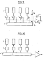
- FIG. 9 represents another embodiment of a mosaic according to the invention.
- the transition from the first to the second step and vice-versa is done sequentially, no longer by a CCD register, but simply by a multiple-output address register R which has several outputs.
- Each output is connected to the gate of a MOS transistor T 41 , T 42 , T 43 ..., which is connected between one of the electrodes e of the second network and a common point R o which receives periodically, through the through a capacitor C i , a pulse i causing the detectors which receive it to pass from one stage to the other.
- the detection substrate 3 and the reading substrate 4 are permanently brought to constant potentials V D and V L.
- the electrodes e can be read in 0 current using, as in the case of FIGS. 6a and 6b, an operational amplifier A mounted as an integrator with a capacity C R.
- the current reading can be done, as in the case of FIGS. 6a and 6b, by integrating the current which circulates in the bias circuit of the detection substrate between the end of the first step and the start of the next first step. It is also possible to integrate the evolution of the current in the bias circuit connected to the electrodes, that is to say at the output of amplifier A.
- the transition from the first to the second stage and vice versa can also be done in parallel, that is to say at the same time for all the detectors. This can be obtained by acting on the polarization of the detection and reading substrates or by acting on the polarization of the electrodes e of the second network which are connected in parallel. In the case of pyroelectric detectors, only the variable polarization of the electrodes e of the second network can be used.
- FIG. 10 represents another embodiment of a mosaic according to the invention in which the passage from one stage to the other takes place in parallel. A CCD register R ′ is then used which ensures lateral transfer, in the direction indicated by an arrow in the figure, of the charge quantities corresponding to the reading carried out at the same instant on the electrodes e.
- This CCD register therefore performs a multiplexed reading of the detectors of a line of the mosaic.
- a preamp Ficitor 10 is connected to this register.
- the register R 'and the preamplifier 10 can be integrated into the read substrate.
- a device f which ensures the conversion of the voltage on each electrode e into charges which can be introduced into the CCD. Indeed, during the integration time t i the electrodes e are floating, that is to say that they are not connected to any bias voltage, their potential therefore evolves and it is this measure of the evolution of the voltage on the electrodes e during the integration time which constitutes the reading signal of the mosaic.
- the conversion of the voltage on the electrodes e into charges in the CCD register can be carried out in various known ways and in particular by the method of equilibration of potentials which is described in the review IEEE, Journal of Solid State Circuits, volume SC 10, Nr. 2, April 1975.
Landscapes
- Engineering & Computer Science (AREA)
- Multimedia (AREA)
- Signal Processing (AREA)
- Transforming Light Signals Into Electric Signals (AREA)
- Solid State Image Pick-Up Elements (AREA)
- Conductive Materials (AREA)
Applications Claiming Priority (2)
| Application Number | Priority Date | Filing Date | Title |
|---|---|---|---|
| FR7916560A FR2460079A1 (fr) | 1979-06-27 | 1979-06-27 | Mosaique de detecteurs de rayonnement lue par un dispositif semi-conducteur, et systeme de prise de vues comportant une telle mosaique |
| FR7916560 | 1979-06-27 |
Publications (1)
| Publication Number | Publication Date |
|---|---|
| EP0021910A1 true EP0021910A1 (fr) | 1981-01-07 |
Family
ID=9227176
Family Applications (1)
| Application Number | Title | Priority Date | Filing Date |
|---|---|---|---|
| EP80400788A Withdrawn EP0021910A1 (fr) | 1979-06-27 | 1980-06-03 | Mosaique de détecteurs de rayonnement lue par un dispositif semiconducteur, et système de prise de vues comportant une telle mosaique |
Country Status (4)
| Country | Link |
|---|---|
| US (1) | US4311906A (OSRAM) |
| EP (1) | EP0021910A1 (OSRAM) |
| JP (1) | JPS5613781A (OSRAM) |
| FR (1) | FR2460079A1 (OSRAM) |
Families Citing this family (5)
| Publication number | Priority date | Publication date | Assignee | Title |
|---|---|---|---|---|
| EP0233866A1 (en) * | 1985-09-03 | 1987-09-02 | FARNUM, Henry Merritt | A universal construction devices for models, stagecraft, models of matrices and the like |
| US4752688A (en) * | 1986-06-18 | 1988-06-21 | Galileo Electro-Optics Corp. | Imaging tube |
| US5340984A (en) * | 1992-05-19 | 1994-08-23 | Skw Corporation | Non-contact interconnect for focal plane arrays |
| US20070236939A1 (en) * | 2006-03-31 | 2007-10-11 | 3M Innovative Properties Company | Structured Composite Optical Films |
| JP2016151523A (ja) * | 2015-02-18 | 2016-08-22 | 浜松ホトニクス株式会社 | 赤外線検出装置 |
Citations (3)
| Publication number | Priority date | Publication date | Assignee | Title |
|---|---|---|---|---|
| GB1258572A (OSRAM) * | 1968-03-07 | 1971-12-30 | ||
| US3973146A (en) * | 1974-03-18 | 1976-08-03 | North American Philips Corporation | Signal detector comprising field effect transistors |
| US4197469A (en) * | 1978-05-25 | 1980-04-08 | Rockwell International Corporation | Capacitively coupled array of photodetectors |
-
1979
- 1979-06-27 FR FR7916560A patent/FR2460079A1/fr active Granted
-
1980
- 1980-06-03 EP EP80400788A patent/EP0021910A1/fr not_active Withdrawn
- 1980-06-24 US US06/162,653 patent/US4311906A/en not_active Expired - Lifetime
- 1980-06-27 JP JP8667880A patent/JPS5613781A/ja active Pending
Patent Citations (3)
| Publication number | Priority date | Publication date | Assignee | Title |
|---|---|---|---|---|
| GB1258572A (OSRAM) * | 1968-03-07 | 1971-12-30 | ||
| US3973146A (en) * | 1974-03-18 | 1976-08-03 | North American Philips Corporation | Signal detector comprising field effect transistors |
| US4197469A (en) * | 1978-05-25 | 1980-04-08 | Rockwell International Corporation | Capacitively coupled array of photodetectors |
Non-Patent Citations (1)
| Title |
|---|
| PROCEEDINGS OF THE IEEE, Vol. 63, No. 1, Janvier 1975 New York US A.J. STECKL et al.: "Application of charge-coupled devices to infrared detection and imaging" pages 67-74. * En entier * * |
Also Published As
| Publication number | Publication date |
|---|---|
| FR2460079B1 (OSRAM) | 1984-08-10 |
| FR2460079A1 (fr) | 1981-01-16 |
| US4311906A (en) | 1982-01-19 |
| JPS5613781A (en) | 1981-02-10 |
Similar Documents
| Publication | Publication Date | Title |
|---|---|---|
| EP0028960B1 (fr) | Matrice de détection d'un rayonnement électromagnétique et intensificateur d'images radiologiques comportant une telle matrice | |
| EP0038725B1 (fr) | Dispositif photosensible lu par transfert de charges, et caméra de télévision comportant un tel dispositif | |
| EP0367650B1 (fr) | Dispositif photosensible du type à amplification du signal au niveau des points photosensibles | |
| EP0153251B1 (fr) | Capteur d'images à barettes multilinéaires à transfert de charges | |
| EP0233104A1 (fr) | Matrice d'élements photosensibles et son procédé de fabrication, procédé de lecture associé, et application de cette matrice à la prise de vue d'images | |
| EP0783227A2 (fr) | Dispositif de lecture de barrettes de détecteurs avec effet TDI | |
| EP0237365A1 (fr) | Dispositif photosensible | |
| FR2598250A1 (fr) | Panneau de prise de vue radiologique, et procede de fabrication | |
| FR2505589A1 (fr) | Appareil analyseur d'images a semi-conducteurs | |
| FR2504334A1 (fr) | Dispositif d'analyse d'image en lignes successives, utilisant le transfert de charges electriques, composant une memoire de ligne, et camera de television comportant un tel dispositif | |
| EP0478457B1 (fr) | Détecteur d'images à l'état solide intégrant un filtre de bruit | |
| EP0021910A1 (fr) | Mosaique de détecteurs de rayonnement lue par un dispositif semiconducteur, et système de prise de vues comportant une telle mosaique | |
| EP0182679B1 (fr) | Dispositif photosensible à transfert de ligne muni d'amplificateurs de contre-réaction | |
| EP0149948B1 (fr) | Perfectionnement aux dispositifs photosensibles à l'état solide | |
| EP0207826B1 (fr) | Dispositif de détection avec retard et intégration en phase | |
| FR2511545A1 (fr) | Dispositif semi-conducteur comportant un dispositif a couplage de charges a quatre phases | |
| EP0958545B1 (fr) | Circuit integrateur de charges photogenerees a linearite amelioree | |
| WO2021043456A1 (fr) | Capteur infrarouge a capture instantanee | |
| FR2561470A1 (fr) | Filtre transversal a couplage de charges | |
| EP0654945B1 (fr) | Circuit d'injection, en imagerie thermique | |
| EP3829160B1 (fr) | Pixel à plage dynamique ajustable pour la réduction de bruit | |
| EP0737002A1 (fr) | Registre de lecture à transfert de charges à sorties multiples | |
| EP0354106A1 (fr) | Circuit d'élimination du bruit, intégré dans un détecteur d'images à l'état solide | |
| EP0028961A1 (fr) | Filtre à transfert de charges et filtre à capacités commutées comportant un multiplicateur de tension à capacités commutées | |
| FR2587864A1 (fr) | Dispositifs imageurs infrarouges |
Legal Events
| Date | Code | Title | Description |
|---|---|---|---|
| PUAI | Public reference made under article 153(3) epc to a published international application that has entered the european phase |
Free format text: ORIGINAL CODE: 0009012 |
|
| AK | Designated contracting states |
Designated state(s): DE GB NL |
|
| 17P | Request for examination filed |
Effective date: 19810117 |
|
| STAA | Information on the status of an ep patent application or granted ep patent |
Free format text: STATUS: THE APPLICATION HAS BEEN WITHDRAWN |
|
| 18W | Application withdrawn |
Withdrawal date: 19830207 |
|
| RIN1 | Information on inventor provided before grant (corrected) |
Inventor name: FELIX, PIERRE Inventor name: LE PARQUIER, GUY |