EP0021908A1 - Charge transfer phase inverter and differential amplifier comprising such a device - Google Patents
Charge transfer phase inverter and differential amplifier comprising such a device Download PDFInfo
- Publication number
- EP0021908A1 EP0021908A1 EP80400786A EP80400786A EP0021908A1 EP 0021908 A1 EP0021908 A1 EP 0021908A1 EP 80400786 A EP80400786 A EP 80400786A EP 80400786 A EP80400786 A EP 80400786A EP 0021908 A1 EP0021908 A1 EP 0021908A1
- Authority
- EP
- European Patent Office
- Prior art keywords
- voltage
- charges
- under
- electrode
- transfer
- Prior art date
- Legal status (The legal status is an assumption and is not a legal conclusion. Google has not performed a legal analysis and makes no representation as to the accuracy of the status listed.)
- Granted
Links
- 238000002347 injection Methods 0.000 claims description 18
- 239000007924 injection Substances 0.000 claims description 18
- 239000000758 substrate Substances 0.000 claims description 9
- 238000011144 upstream manufacturing Methods 0.000 claims description 6
- 239000004065 semiconductor Substances 0.000 claims description 3
- 238000012423 maintenance Methods 0.000 claims 1
- 238000010586 diagram Methods 0.000 description 7
- 238000006243 chemical reaction Methods 0.000 description 3
- 230000003071 parasitic effect Effects 0.000 description 3
- VYPSYNLAJGMNEJ-UHFFFAOYSA-N Silicium dioxide Chemical compound O=[Si]=O VYPSYNLAJGMNEJ-UHFFFAOYSA-N 0.000 description 1
- 240000008042 Zea mays Species 0.000 description 1
- 230000015572 biosynthetic process Effects 0.000 description 1
- 239000000969 carrier Substances 0.000 description 1
- 239000002800 charge carrier Substances 0.000 description 1
- 238000009792 diffusion process Methods 0.000 description 1
- 230000007717 exclusion Effects 0.000 description 1
- 238000002513 implantation Methods 0.000 description 1
- 239000012212 insulator Substances 0.000 description 1
- 230000010354 integration Effects 0.000 description 1
- 150000002500 ions Chemical class 0.000 description 1
- 238000002955 isolation Methods 0.000 description 1
- 244000045947 parasite Species 0.000 description 1
- 230000000737 periodic effect Effects 0.000 description 1
- 230000010287 polarization Effects 0.000 description 1
- 229910052710 silicon Inorganic materials 0.000 description 1
- 239000010703 silicon Substances 0.000 description 1
- 229910052814 silicon oxide Inorganic materials 0.000 description 1
Images
Classifications
-
- H—ELECTRICITY
- H03—ELECTRONIC CIRCUITRY
- H03H—IMPEDANCE NETWORKS, e.g. RESONANT CIRCUITS; RESONATORS
- H03H15/00—Transversal filters
-
- H—ELECTRICITY
- H03—ELECTRONIC CIRCUITRY
- H03F—AMPLIFIERS
- H03F3/00—Amplifiers with only discharge tubes or only semiconductor devices as amplifying elements
- H03F3/005—Amplifiers with only discharge tubes or only semiconductor devices as amplifying elements using switched capacitors, e.g. dynamic amplifiers; using switched capacitors as resistors in differential amplifiers
Definitions
- the present invention relates to a charge transfer phase reversing device.
- the signal to be inverted is generally converted into voltage, then the phase inversion is created into voltage and the voltage variations are re-injected into charges in the charge transfer device.
- the conversions of charges into voltage and vice versa have the disadvantage of being not very linear and of gain which is difficult to reproduce.
- the devices making it possible to carry out these conversions and the phase-to-voltage inversion are generally bulky and of high consumption.
- the present invention relates to a device which performs the phase inversion of a signal while remaining in the field of loads.
- This device has the advantage of being easily integrated into a more complex charge transfer device. It allows to obtain with good precision two signals in phase opposition. In a preferred embodiment, this device does not require, in addition to the DC input voltage which is applied to several transfer electrodes and storage, only three clock signals which ensure the transfer of charges, which increases its simplicity and precision.
- the device according to the invention makes it possible in particular to produce a differential amplifier which does not require conversion of the charges into voltage and which therefore has, compared with the differential amplifiers according to known art, advantages from the point of view of consumption and integration.
- the present invention relates to a charge transfer phase reversing device which receives an input voltage V e constituted by the superposition of a direct voltage V o and a time-varying and sampled voltage v e and which comprises means making the difference between the quantity of charges double that corresponding to the direct voltage V o and the quantity of charges corresponding to each sample of the variable voltage V e superimposed on the direct voltage.
- V e an input voltage
- V o constituted by the superposition of a direct voltage V o and a time-varying and sampled voltage v e
- V e V o ⁇ V e .
- Q e Q avg ⁇ q e .
- the device according to the invention therefore allows to obtain, from a quantity of charges Q avg + q e , a quantity of charges Q avg - qe and vice versa. A phase inversion on the charges is therefore carried out.
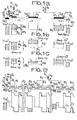
- Figure 1a shows a cross-sectional view of an embodiment of the device according to the invention.
- the device according to the invention is produced on a semiconductor substrate 1, of type P silicon in the example, covered with an insulating layer, of silicon oxide in the example, which is not shown in the Figure 1a. On this insulating layer, alternate charge storage and transfer electrodes which are arranged substantially normally in the direction of charge propagation. The transfer electrodes are deposited on an insulating thickness which is not shown in FIG. 1a.
- this arrangement has a double function, on the one hand ensuring the continuity of the potentials created in the semiconductor 1, and on the other hand imposing a single transfer direction for the charge carriers.
- This structure comprising an extra thickness of insulator can be replaced by an overdoping of the substrate, by implantation of ions, ensuring the same functions.
- FIG. 1a only the transfer and storage electrodes constituting the phase reversing device according to the invention have been shown, with the exclusion of the transfer and storage electrodes ensuring only the transfer of the charges.
- the means performing the subtraction include in particular a first and a second storage electrodes G1 and G 2 electrically connected at a point P which can be connected to the voltage continuous V 0 or which can be left floating, i.e. not connected to any voltage source.
- a switch K symbolically represents the two possibilities of polarization of point P.
- a transfer electrode G o1 Upstream of the first storage electrode, in the direction of charge transfer indicated by an arrow, is a transfer electrode G o1 , brought to a constant voltage V T , and a charge injection diode D e1 , connected at a variable voltage V D.
- the point P is connected to the constant voltage V o .
- the voltage V D applied to the diode D e1 is successively lower then greater than the surface potential V ref under the transfer electrode G o1 connected to V T.
- a quantity of reference charges Q ref is thus stored under the storage electrode G 1 .
- the phase reversing device further comprises a third storage electrode G e located upstream of the second, G 2 , in the direction of charge transfer indicated by an arrow.
- This third storage electrode G e receives the input voltage V e at a point O. Between the point O and a point N, is connected a resistance R. Between the point O and a point M, is connected a capacitance C. The DC input voltage V o is applied to the point N and the voltage variable in time and sampled V e is applied to point M.
- a transfer electrode G Oe carried, as G o1 , at constant voltage V T and a charge injection diode D e2 , carried as D e1 , at the variable voltage V D.
- FIGs 1a, b, c there are shown diagrams illustrating the operation of the device according to the invention. These diagrams represent the evolution of the surface potential ⁇ s in the substrate 1. The hatched areas indicate the presence of minority carriers.
- FIG. 1a illustrates the injection of a quantity of charges Q ref under the electrode G 1 and a quantity of charges Q under the electrode G.
- the injection of charges under the electrodes G 1 and G 2 is done in the same way.
- the transfer electrodes G o1 and G oe are connected to the constant voltage V T which fixes the surface potential under G 1 and G e at the maximum value V ref .
- the voltage V D applied to the diodes D e1 and D e2 successively takes a value lower then higher than the surface potential V ref , which causes the storage of the quantities of charges Q ref and Q e under G 1 and G e .
- the quantity of charges stored under G 1 , Q ref must be equal to twice the quantity of charges Q avg corresponding to the DC input voltage V o .
- the quantity of charges Q injected under the electrode G e which receives the voltage V V o ⁇ v e is written: is a constant which depends on V ref and on physical characteristics which are the same for the whole of the charge transfer device on which the inverter is made and where C e represents the oxide capacity of the electrode G e .
- the quantity of charges Q avg therefore equals (V o - V a ) C e .
- the storage electrode G 1 is generally given a surface twice that of G e , which can be achieved with good precision.
- V T the constant voltage applied to the transfer electrodes G o1 and G Oe , equal to the DC input voltage V o .
- FIG. 1a represents the surface potentials under the device according to the invention in the case where V equals V o and in the case where the surface of the electrode G 1 is twice that of the electrode G e .
- the input voltage V e can vary around V o between Va and 2 V o - Va.
- the surface potential under Geav before the charge injection can therefore vary by the same amount ⁇ 0 around ⁇ o .
- the variation in surface potential ⁇ under the second storage electrode G 2 depends, for a given quantity of charges Q e , on the relative values of the oxide capacities C 1 and C 2 of the storage electrodes G 1 and G 2 .
- the potential well created under the second storage electrode G 2 must be sufficient for the maximum quantity of charges Q max , injected under G e and corresponding to a well depth under Ge before injection of charges equal to ⁇ o + ⁇ ⁇ o , can be stored there.
- the oxide capacity of G 2 (and therefore the surface of G 2 ) is chosen such that:
- FIGS. 1a, b, c represent the surface potentials in the substrate in the case where:
- the variations in surface potential under G 2 , ⁇ are equal to the variations in surface potential under G e , ⁇ ⁇ e .
- FIG. 1b represents the surface potentials in the case where the quantity of charges injected Q e equals:
- FIG. 1c represents the surface potentials in the substrate in the case where
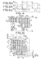
- FIG. 2 shows a cross-sectional view showing the device shown in Figure 1a inserted in a more complex load transfer device, as well as a diagram illustrating the transfer of loads.
- pairs of transfer electrode G o - storage electrode G which ensure the transfer of the charges, are added to the device according to the invention represented in FIG. 1a between the grids G e and G 2 , after the electrode G 2 and after electrode G 1 .
- the transfer electrode G 02 which precedes G 2 is brought to a constant voltage Vu less than V o to increase the depth of the well under G2.
- FIGS. 3a, b, c represent diagrams of signals which can be applied to the device shown in FIG. 2.
- These clock signals ⁇ 1 , ⁇ 2 and ⁇ 3 are periodic functions of the same period T, the amplitude of which varies between a low level and a high level.
- the signals ⁇ 1 and ⁇ 2 are practically in phase opposition, with however a slight overlap at the high level as is customary in the field of charge transfers.
- the signal ⁇ 3 goes high while ⁇ 1 is already there and returns to the low level before ⁇ 1 .
- the signal ⁇ 1 is applied to the diodes D e1 and D e2 , as well as to a transfer electrode-storage electrode pair out of two, and in particular to that which follows the electrode G e .
- the signal ⁇ 2 is applied to the MOS transistor T 1 , connected between the point P and the voltage V o , and which replaces the switch K shown in FIG. 1a.
- the ⁇ 2 signal is also applied to a torque transfer electrode - on two storage electrode, and in particular to that which precedes the torque transfer electrode G02 - storage electrode G 2.
- the signal ⁇ 3 is applied to the pair of electrodes following the storage electrodes G 1 and G2.
- the signal ⁇ 2 is at the high level and the signals ⁇ 1 and ⁇ 3 are at the low level.
- the surface potentials in the substrate are shown in Figure 2 in solid lines.
- the electrodes G 1 and G 2 receive by the transistor T 1 which is made conductive the direct voltage V o .
- the passage from ⁇ 1 to the low level causes the diodes to inject the quantities of charges Q ref and Q e under G 1 and Ge These quantities of charges are blocked under G 1 and G e by the pairs of electrodes along G 1 and G e which are at the low level.
- the signal ⁇ 1 is at the high level and the signals ⁇ 2 and ⁇ 3 are at the low level.
- the potentials in the substrate are shown in broken lines in FIG. 2.
- the pair of electrodes preceding the pair of transfer electrode G o2 - storage electrode G 2 ensures the transfer under G 2 of the quantity of charges Q e , and thus the formation of the quantity of charges Q avg Q e , corresponding to the signal reversed in phase under the electrode G 1 .
- the signals ⁇ 1 and ⁇ 3 are at the high level and the signal ⁇ 2 is at the low level.
- the surface potentials in the substrate are shown in dotted lines in FIG. 2.
- the pairs of electrodes along G 1 and G 2 which are brought to the high level, ensure the evacuation of the charges stored under G 1 and under G 2 .
- the device according to the invention is thus ready to receive at time t 1 according to a new quantity of charges Q e corresponding to a sample of the input voltage under the electrode G. e
- FIG. 4 represents a top view of a device similar to that of FIG. 2.
- the storage electrodes G e and G 2 on the one hand, and G 1 on the other hand, are produced in two parallel charge transfer channels 2 and 3.
- the channel 2 delivers charge quantities corresponding to the input voltage V e and channel 3 delivers quantities of charges corresponding to the input voltage reversed in phase.
- the device shown in FIG. 4 has the advantage, from the point of view of practical implementation, of having a reduced bulk.
- FIG. 5 represents a top view of a differential amplifier according to the invention.
- the device shown in FIG. 5 includes a phase reversing device as previously described, which reverses the phase of one of the two input voltages of the differential amplifier, ie V e this voltage.
- the differential amplifier according to the invention comprises several charge transfer channels isolated by isolation and parallel diffusions. It notably includes channels 2 and 3 identical to those shown in FIG. 4. Channel 2 receives the input voltage to be inverted V and transfers the charge to be inverted Q e . Channel 3 generates the reverse signal load - Q and transfers it.
- the differential amplifier according to the invention also comprises a channel 4 which receives the second input voltage from the differential amplifier V e + and which transfers the charge Q e + .
- a channel 5 joins channels 3 and 4 and adds the charges Q e + and - Q e - . These charges are transferred to channel 5 and read on floating diodes D 1 and D 2 . connected to a follower stage, as is known.
- Channel 4 includes a charge injection device identical to that of channel 2. This device consists in particular of a charge injection diode D e3 and a storage electrode G ' e to which the input voltage V e + of the differential amplifier.
- phase reversing device depends above all on the parasitic capacitance Cp existing at point P where the first and second storage electrodes G 1 and G 2 are connected.
- the parasitic capacitance Cp means that the quantity of charges which is removed from G 2 when Q e arrives - under G 1 is not equal to Q e - but to ⁇ Q e - which is defined:
- the quantity of initial charges Q initial under G 1 is equal to 2 Q avg .
- the quantity of final charges Q under G 1 is therefore expressed:
- the final quantity of charges under the electrode G 1 therefore consists of a constant term (2- ⁇ ) Q avg and a variable term + ⁇ q e -.
- the error in g entered by the coefficient ⁇ on the variable term can be compensated for by injecting the quantity of charges Q + on channel 4 with an attenuation factor ⁇
- the differential amplifier according to the invention therefore has a rejection in common mode whose efficiency depends only on the precision with which the parasitic capacitance C p and therefore the coefficient ⁇ can be determined.
Landscapes
- Engineering & Computer Science (AREA)
- Power Engineering (AREA)
- Solid State Image Pick-Up Elements (AREA)
- Amplifiers (AREA)
Abstract
Dispositif inverseur de phase à transfert de charges dont la tension d'entrée Ve est constituée par la superposition d'une tension continue Vo et d'une tension variable dans le temps et échantillonnée ve. On effectue la soustraction entre la quantité de charges double de celle correspondant à la tension continue, soit 2 Qmoy, et la quantité de charges correspondant à chaque échantillon de la tension variable superposé à la tension continue, soit Qmoy ? qe.Charge transfer phase reversing device, the input voltage Ve of which is constituted by the superposition of a direct voltage Vo and a voltage variable over time and sampled ve. We perform the subtraction between the quantity of charges double that corresponding to the DC voltage, ie 2 Qmoy, and the quantity of charges corresponding to each sample of the variable voltage superimposed on the DC voltage, ie Qmoy? qe.
Description
. La présente invention concerne un dispositif inverseur de phase à transfert de charges.. The present invention relates to a charge transfer phase reversing device.
Elle concerne également un amplificateur différentiel comportant un tel dispositif.It also relates to a differential amplifier comprising such a device.
Lors du traitement par transfert de charges de signaux analogiques, il est souvent nécessaire de produire des signaux en opposition de phase. C'est le cas, par exemple, dans les amplificateurs différentiels utilisés notamment dans l'étage de sortie des filtres à transfert de charges.When processing by charge transfer of analog signals, it is often necessary to produce signals in phase opposition. This is the case, for example, in the differential amplifiers used in particular in the output stage of the charge transfer filters.
Dans l'art antérieur, on convertit généralement le signal à inverser en tension, puis, on crée l'inversion de phase en tension et on ré-injecte en charges dans le dispositif à transfert de charges les variations de tension.In the prior art, the signal to be inverted is generally converted into voltage, then the phase inversion is created into voltage and the voltage variations are re-injected into charges in the charge transfer device.
Les conversions de charges en tension et vice-versa présentent l'inconvénient d'être peu linéaires et de gain difficilement reproductible. D'autre part, les dispositifs permettant de réaliser ces conversions et l'inversion de phase en tension sont généralement encombrants et de consommation-élevée.The conversions of charges into voltage and vice versa have the disadvantage of being not very linear and of gain which is difficult to reproduce. On the other hand, the devices making it possible to carry out these conversions and the phase-to-voltage inversion are generally bulky and of high consumption.
La présente invention concerne un dispositif qui réalise l'inversion de phase d'un signal en restant dans le domaine des charges.The present invention relates to a device which performs the phase inversion of a signal while remaining in the field of loads.
Ce dispositif présente l'avantage d'être facilement intégrable dans un dispositif à transfert de charges plus complexe. Il permet d'obtenir avec une bonne précision deux signaux en opposition de phase. Dans un mode de réalisation préféré, ce dispositif ne nécessite, outre la tension continue d'entrée qui est appliquée à plusieurs électrodes de transfert et de stockage, que trois signaux d'horloge qui assurent le transfert des charges, ce qui accroît sa simplicité et sa précision.This device has the advantage of being easily integrated into a more complex charge transfer device. It allows to obtain with good precision two signals in phase opposition. In a preferred embodiment, this device does not require, in addition to the DC input voltage which is applied to several transfer electrodes and storage, only three clock signals which ensure the transfer of charges, which increases its simplicity and precision.
Le dispositif selon l'invention permet notamment de réaliser un amplificateur différentiel qui ne nécessite pas de conversion des charges en tension et qui présente donc par rapport aux amplificateurs différentiels selon l'art connu des avantages au point de vue de la consommation et de l'intégration.The device according to the invention makes it possible in particular to produce a differential amplifier which does not require conversion of the charges into voltage and which therefore has, compared with the differential amplifiers according to known art, advantages from the point of view of consumption and integration.
La présente invention concerne un dispositif inverseur de phase à transfert de charges qui reçoit une tension d'entrée Ve constituée par la superposition d'une tension continue Vo et d'une tension variable dans le temps et échantillonnée ve et qui comporte des moyens effectuant la différence entre la quantité de charges double de celle correspondant à la tension continue Vo et la quantité de charges correspondant à chaque échantillon de la tension variable Ve superposée à la tension continue. Ainsi se trouvent élaborés des paquets de charges correspondant à une tension en opposition de phase avec la tension d'entrée V . eThe present invention relates to a charge transfer phase reversing device which receives an input voltage V e constituted by the superposition of a direct voltage V o and a time-varying and sampled voltage v e and which comprises means making the difference between the quantity of charges double that corresponding to the direct voltage V o and the quantity of charges corresponding to each sample of the variable voltage V e superimposed on the direct voltage. Thus packets of charges are produced corresponding to a voltage in phase opposition with the input voltage V. e
La tension d'entrée V s'écrit : Ve = Vo ± Ve. Après injection dans le dispositif, la quantité de charges Qe correspondant à la tension Ve s'écrit : Qe = Qmoy ± qe. Selon l'invention, des moyens effectuent la différence entre 2 Q moy et Q . e The input voltage V is written: V e = V o ± V e . After injection into the device, the quantity of charges Q e corresponding to the voltage V e is written: Q e = Q avg ± q e . According to the invention, means make the difference between 2 Q avg and Q. e
Lorsque Qe est supérieur à Qmoy (Qe = Qmoy + qe), le résultat de cette soustraction s'écrit :![]()
![]()
Lorsque Qe est inférieur à Q moy (Qe = Q moy - qe), le résultat de cette soustraction s'écrit :![]()
![]()
Le dispositif selon l'invention permet donc d'obtenir, à partir d'une quantité de charges Qmoy + qe, une quantité de charges Qmoy - q e et vice-versa. Une inversion de phase sur les charges est donc réalisée.The device according to the invention therefore allows to obtain, from a quantity of charges Q avg + q e , a quantity of charges Q avg - qe and vice versa. A phase inversion on the charges is therefore carried out.
La description suivante donne, à titre d'exemple, un mode de réalisation des moyens effectuant la soustraction selon l'invention.The following description gives, by way of example, an embodiment of the means performing the subtraction according to the invention.
D'autres objets, caractéristiques et résultats de l'invention ressortiront de la description suivante, donnée à titre d'exemple non limitatif et illustrée par les figures annexées qui représentent :
- - les figures 1a, b, c, une vue en coupe transversale d'un mode de réalisation du dispositif selon l'invention et des schémas illustrant son fonctionnement ;
- - la figure 2, une vue en coupe transversale montrant le dispositif représenté sur la figure 1a inséré dans un dispositif à transfert de charges plus complexe et un schéma illustrant le transfert des charges ;
- - les figures 3a, b, c, des diagrammes de si- gnauxsusceptibles d'être appliqués au dispositif représenté sur la figure 2 ;
- - la figure 4, une vue de dessus d'un dispositif analogue à celui de la figure 2 ;
- - la figure 5, une vue de dessus d'un amplificateur différentiel selon l'invention.
- - Figures 1a, b, c, a cross-sectional view of an embodiment of the device according to the invention and diagrams illustrating its operation;
- - Figure 2, a cross-sectional view showing the device shown in Figure 1a inserted in a more complex load transfer device and a diagram illustrating the transfer of loads;
- FIGS. 3a, b, c, diagrams of signals which can be applied to the device shown in FIG. 2;
- - Figure 4, a top view of a device similar to that of Figure 2;
- - Figure 5, a top view of a differential amplifier according to the invention.
Sur les différentes figures, les mêmes reprères désignent les mêmes éléments, mais, pour des raisons de clarté, les cotes et proportions des différents éléments n'ont pas été respectées.In the different figures, the same references designate the same elements, but, for reasons of clarity, the dimensions and proportions of the different elements have not been respected.
La figure 1a représente une vue en coupe transversale d'un mode de réalisation du dispositif selon l'invention.Figure 1a shows a cross-sectional view of an embodiment of the device according to the invention.
Le dispositif selon l'invention est réalisé sur un substrat semi-conducteur 1, en silicium de type P dans l'exemple, recouvert d'une couche isolante, en oxyde de silicium dans l'exemple, qui n'est pas représentée sur la figure 1a. Sur cette couche isolante, alternent des électrodes de stockage et de transfert de charges qui sont disposées sensiblement normalement à la direction de propagation des charges. Les électrodes de transfert sont déposées sur une surépaisseur d'isolant qui n'est pas représentée sur la figure 1a.The device according to the invention is produced on a semiconductor substrate 1, of type P silicon in the example, covered with an insulating layer, of silicon oxide in the example, which is not shown in the Figure 1a. On this insulating layer, alternate charge storage and transfer electrodes which are arranged substantially normally in the direction of charge propagation. The transfer electrodes are deposited on an insulating thickness which is not shown in FIG. 1a.
Ainsi qu'il est connu, cette disposition a une double fonction, d'une part assurer la continuité des potentiels créés dans le semi-conducteur 1, et d'autre part imposer un sens de transfert unique pour les porteurs de charges.As is known, this arrangement has a double function, on the one hand ensuring the continuity of the potentials created in the semiconductor 1, and on the other hand imposing a single transfer direction for the charge carriers.
Cette structure comportant une surépaisseur d'isolant peut être remplacée par un surdopage du substrat, par implantation d'ions, assurant les mêmes fonctions.This structure comprising an extra thickness of insulator can be replaced by an overdoping of the substrate, by implantation of ions, ensuring the same functions.
Sur-la figure 1a, on n'a représenté que les électrodes de transfert et de stockage constituant le dispositif inverseur de phase selon l'invention à l'exclusion des électrodes de transfert et de stockage assurant uniquement le transfert des charges.In FIG. 1a, only the transfer and storage electrodes constituting the phase reversing device according to the invention have been shown, with the exclusion of the transfer and storage electrodes ensuring only the transfer of the charges.
1 Dans le mode de réalisation du dispositif selon l'invention représenté sur la figure 1a, les moyens effectuant la soustraction comportent notamment une première et une deuxième électrodes de stockage G1 et G2 connectées électriquement en un point P qui peut être relié à la tension continue V0 ou qui peut être laissé flottant, c'est-à-dire n'être relié à aucune source de tension. Sur la figure, un interrupteur K représente symboliquement les deux possibilités de polarisation du point P.1 In the embodiment of the device according to the invention shown in FIG. 1a, the means performing the subtraction include in particular a first and a second storage electrodes G1 and G 2 electrically connected at a point P which can be connected to the voltage continuous V 0 or which can be left floating, i.e. not connected to any voltage source. In the figure, a switch K symbolically represents the two possibilities of polarization of point P.
En amont de la première électrode de stockage, selon le sens de transfert des charges indiqué par une flèche, se trouve une électrode de transfert Go1, portée à une tension constante VT, et une diode d'injection de charges De1, reliée à une tension variable VD.Upstream of the first storage electrode, in the direction of charge transfer indicated by an arrow, is a transfer electrode G o1 , brought to a constant voltage V T , and a charge injection diode D e1 , connected at a variable voltage V D.
On connaît, dans l'art antérieur, le fonctionnement d'un dispositif constitué par les électrodes G1, G2, Go1 et par la diode De1.The operation of a device constituted by the electrodes G 1 , G 2 , G o1 and by the diode D e1 is known in the prior art.
Dans un premier temps, le point P est relié à la tension constante Vo. Avant l'arrivée des charges sous l'électrode de stockage G2, la tension VD appliquée à la diode De1 est successivement inférieure puis supérieure au potentiel de surface Vréf sous l'électrode de transfert Go1 reliée à VT. Une quantité de charges de référence Qréf est ainsi stockée sous l'électrode de stockage G1.First, the point P is connected to the constant voltage V o . Before the arrival of the charges under the storage electrode G 2 , the voltage V D applied to the diode D e1 is successively lower then greater than the surface potential V ref under the transfer electrode G o1 connected to V T. A quantity of reference charges Q ref is thus stored under the storage electrode G 1 .
Dans un deuxième temps, le point P est laissé flottant. Lors de l'arrivée d'une quantité de charges Qe sous G2, le potentiel de surface sous G1 est maintenu constant à la valeur Vréf par Go1 et l'excédent de charges est envoyé sous la diode De1. On démontre que la quantité de charges se trouvant sous De1 à la fin de ce deuxième temps est sensiblement égale à Qréf - Qe (il faut pour cela négliger la capacité de déplétion sous G2 devant les capacités d'oxyde de G1 et G2).Secondly, point P is left floating. When a quantity of charges Q e arrives under G 2 , the surface potential under G 1 is kept constant at the value V ref by G o1 and the excess charges is sent under the diode D e1 . It is shown that the quantity of charges found under D e1 at the end of this second time is substantially equal to Q ref - Q e (this requires neglecting the depletion capacity under G 2 compared to the oxide capacities of G1 and G 2 ).
Le dispositif inverseur de phase selon l'invention comporte, en outre, une troisième électrode de stockage Ge située en amont de la deuxième, G2, selon le sens de transfert des charges indiqué par une flèche.Cette troisième électrode de stockage Ge reçoit la tension d'entrée Ve en un point O. Entre le point O et un point N, est reliée une résistance R. Entre le point O et un point M, est reliée une capacité C. La tension continue d'entrée Vo est appliquée au point N et la tension variable dans le temps et échantillonnée Ve est appliquée au point M.The phase reversing device according to the invention further comprises a third storage electrode G e located upstream of the second, G 2 , in the direction of charge transfer indicated by an arrow. This third storage electrode G e receives the input voltage V e at a point O. Between the point O and a point N, is connected a resistance R. Between the point O and a point M, is connected a capacitance C. The DC input voltage V o is applied to the point N and the voltage variable in time and sampled V e is applied to point M.
En amont de la troisième électrode de stockage G selon le sens de transfert des charges, se trouve une électrode de transfert GOe portée, comme Go1, à la tension constante VT et une diode d'injection de charges De2, portée comme De1, à la tension variable VD.Upstream of the third storage electrode G in the direction of charge transfer, there is a transfer electrode G Oe carried, as G o1 , at constant voltage V T and a charge injection diode D e2 , carried as D e1 , at the variable voltage V D.
Selon l'invention, on rappelle qu'on doit effectuer la soustraction entre la quantité de charges double de celle correspondant à la tension continue V0 et la quantité de charges correspondant à chaque échantillon de la tension variable Ve superposée à la tension continue. On injecte donc sous G1 une quantité de charges double de celle correspondant à la tension continue Vo, avant l'arrivée d'un échantillon sous la deuxième électrode de stockage G2 et alors que le point P est à la tension constante Vo. On maintient ensuite le potentiel de surface constant sous la première électrode de stockage G1, lors de l'arrivée d'un échantillon sous la deuxième électrode de stockage G2 et alors que le point P est laissé flottant.According to the invention, it is recalled that the subtraction between the quantity of charges double that corresponding to the DC voltage V 0 and the quantity of charges corresponding to each sample of the variable voltage V e superimposed on the DC voltage must be carried out. A quantity of charges is therefore injected under G 1 twice that corresponding to the direct voltage V o , before the arrival of a sample under the second storage electrode G 2 and while the point P is at the constant voltage V o . The surface potential is then kept constant under the first storage electrode G 1 , when a sample arrives under the second storage electrode G 2 and while the point P is left floating.
Sur les figures 1a, b,c, on a représenté des schémas illustrant le fonctionnement du dispositif selon l'invention. Ces schémas représentent l'évolution du potentiel dé surface φs dans le substrat 1. Les zones hachurées indiquent la présence de porteurs minoritaires.In Figures 1a, b, c, there are shown diagrams illustrating the operation of the device according to the invention. These diagrams represent the evolution of the surface potential φ s in the substrate 1. The hatched areas indicate the presence of minority carriers.
La figure 1a illustre l'injection d'une quantité de charges Qref sous l'électrode G1 et d'une quantité de charges Q sous l'électrode G . L'injection de charges sous les électrodes G1 et G2 se fait de la même façon. Les électrodes de transfert Go1 et Goe sont reliées à la tension constante VT qui fixe le potentiel de surface sous G1 et Ge à la valeur maximale Vref. La tension VD appliquée aux diodes De1 et De2 prend successivement une valeur inférieure puis supérieure au potentiel de surface Vref, ce qui provoque le stockage des quantités de charges Qref et Qe sous G1 et Ge. Cette variation de la tension VD appliquée aux diodes se produit d'une part alors que le point P est relié à la tension constante Vo et avant l'arrivée d'un échantillon sous la deuxième électrode de stockage G2, et d'autre part, alors qu'un échantillon de la tension variable ve est appliquée au point M.FIG. 1a illustrates the injection of a quantity of charges Q ref under the electrode G 1 and a quantity of charges Q under the electrode G. The injection of charges under the electrodes G 1 and G 2 is done in the same way. The transfer electrodes G o1 and G oe are connected to the constant voltage V T which fixes the surface potential under G 1 and G e at the maximum value V ref . The voltage V D applied to the diodes D e1 and D e2 successively takes a value lower then higher than the surface potential V ref , which causes the storage of the quantities of charges Q ref and Q e under G 1 and G e . This variation in the voltage V D applied to the diodes occurs on the one hand while the point P is connected to the constant voltage V o and before the arrival of a sample under the second storage electrode G 2 , and d on the other hand, while a sample of the variable voltage v e is applied at point M.
Selon l'invention, la quantité de charges stockée sous G1, Qref doit être égale au double de la quantité de charges Qmoy correspondant à la tension continue d'entrée Vo.According to the invention, the quantity of charges stored under G 1 , Q ref must be equal to twice the quantity of charges Q avg corresponding to the DC input voltage V o .
La quantité de charges Q injectée sous l'électrode Ge qui reçoit la tension V = Vo ± ve s'écrit :![]()
![]()
D'autre part, la quantité de charges Qréf injectée sous l'électrode G1 qui reçoit la tension Vo s'écrit :
- Qréf = (VO - VA) C1, où C1 représente la capacité d'oxyde de l'électrode G1.
- Q ref = (V O - V A ) C 1 , where C 1 represents the oxide capacity of the electrode G 1 .
Lorsque le point P reçoit une tension constante égale à Vo, il suffit de choisir la capacité d'oxyde C1 double de C e pour que Qréf égale 2 Qmoy, ce qui est le résultat recherché.When point P receives a constant voltage equal to V o , it suffices to choose the oxide capacity C 1 double of C e so that Q ref equals 2 Q avg , which is the desired result.
Pour choisir la capacité d'oxyde C1 double de Ce, on donne généralement à l'électrode de stockage G1 une surface double de celle de Ge, ce qui peut être réalisé avec une bonne précision.To choose the double oxide capacity C 1 of C e , the storage electrode G 1 is generally given a surface twice that of G e , which can be achieved with good precision.
La précision du dispositif selon l'invention dépend en effet de l'égalité des charges 2 Q moy et Qréf.The precision of the device according to the invention indeed depends on the equality of the charges 2 Q avg and Q ref .
Il est possible, pour diminuer le nombre de tensions de polarisation du dispositif selon l'invention de choisir VT, la tension constante appliquée aux électrodes de transfert Go1 et GOe, égale à la tension continue d'entrée Vo.It is possible, to reduce the number of bias voltages of the device according to the invention, to choose V T , the constant voltage applied to the transfer electrodes G o1 and G Oe , equal to the DC input voltage V o .
Après injection de la quantité de charges Qréf = 2 Qmoy, le point P est laissé flottant. Le potentiel de surface sous la première électrode de stockage G1 est maintenu constant à la valeur Vréf par l'électrode de transfert Go1 portée à la tension constante VT (qui peut être égale à Vo). La diode d'injection D e1 est portée à une tension supérieure au potentiel de surface Vréf. La quantité de charges Qe est transférée sous la deuxième électrode de stockage G2. Lors de l'arrivée de la quantité de charges Qe sous G2, une quantité de charges équivalente est soustraite de Qréf stockée sous G1 et éva- cuée vers la diode De1. Il reste donc sous G1 la quantité de charges QS telle que : QS = 2 Qmoy - Qe, ce qui est bien le résultat recherché.After injection of the quantity of charges Q ref = 2 Q avg , the point P is left floating. The surface potential under the first storage electrode G 1 is kept constant at the value V ref by the transfer electrode G o1 brought to the constant voltage V T (which can be equal to V o ). The injection diode D e1 is brought to a voltage greater than the surface potential V ref . The quantity of charges Q e is transferred under the second storage electrode G 2 . When the quantity of charges Q e arrives under G 2 , an equivalent quantity of charges is subtracted from Q ref stored under G 1 and discharged towards the diode D e1 . It therefore remains under G 1 the quantity of charges Q S such that: Q S = 2 Q avg - Q e , which is indeed the desired result.
.La figure 1a représente les potentiels de surface sous le dispositif selon l'invention dans le cas où V égale Vo et dans le cas où la surface de l'électrode G1 est double de celle de l'électrode Ge.FIG. 1a represents the surface potentials under the device according to the invention in the case where V equals V o and in the case where the surface of the electrode G 1 is twice that of the electrode G e .
La tension d'entrée Ve peut varier autour de Vo entre Va et 2 Vo - Va. Le potentiel de surface sous Geavant l'injection des charges peut donc varier d'une même quantité Δφ0 autour de φo.The input voltage V e can vary around V o between Va and 2 V o - Va. The surface potential under Geav before the charge injection can therefore vary by the same amount Δφ 0 around φ o .
La variation de potentiel de surface Δφ sous la deuxième électrode de stockage G2 dépend, pour une quantité de charges Qe donnée, des valeurs relatives des capacités d'oxyde C1 et C2 des électrodes de stockage G1 et G2.The variation in surface potential Δφ under the second storage electrode G 2 depends, for a given quantity of charges Q e , on the relative values of the oxide capacities C 1 and C 2 of the storage electrodes G 1 and G 2 .
En première approximation, la profondeur du puits de potentiel ΔVe sous l'électrode Ge à partir du niveau Vréf s'écrit : ΔVe ≃ ![]()
![]()
L'écriture des relations en charges au point P et sous l'électrode G2, après injection de la quantité de-charges Qréf sous l'électrode G1 et après injection de la quantité de charges Qe sous l'électrode G2, permet d'obtenir l'expression de Δφ suivante, dans laquelle la capacité de déplétion sous G2 est négligée : ;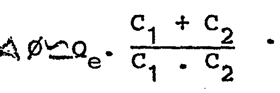
Le puits de potentiel créé sous la deuxième électrode de stockage G2 doit être suffisant pour que la quantité de charges maximale Qmax, injectée sous Ge et correspondant à une profondeur de puits sous Ge avant injection des charges égale à φo + Δ φo, puisse y être stockée.The potential well created under the second storage electrode G 2 must be sufficient for the maximum quantity of charges Q max , injected under G e and corresponding to a well depth under Ge before injection of charges equal to φ o + Δ φ o , can be stored there.
Pour minimiser la variation de potentiel de surface Δφ sous G2, on choisit la capacité d'oxyde de G2 (et donc la surface de G2) telle que :![]()
![]()
Les figures 1a, b, c représentent les potentiels de surface dans le substrat dans le cas où :![]()
![]()
Dans ce cas et toujours en première approximation, les variations de potentiel de surface sous G2, Δφ, sont égales aux variations de potentiel de surface sous Ge, Δ φe.In this case and always as a first approximation, the variations in surface potential under G 2 , Δφ, are equal to the variations in surface potential under G e , Δ φ e .
La figure 1b représente les potentiels de surface dans le cas où la quantité de charges injectée Qe égale :![]()
![]()
La figure 1c représente les potentiels de surface dans le substrat dans le cas où![]()
![]()
La figure 2 représente une vue en coupe transversale montrant le dispositif représenté sur la figure 1a inséré dans un dispositif à transfert de charges plus complexe, ainsi qu'un schéma illustrant le transfert des charges.2 shows a cross-sectional view showing the device shown in Figure 1a inserted in a more complex load transfer device, as well as a diagram illustrating the transfer of loads.
Sur la figure 2, des couples électrode de transfert Go - électrode de stockage G, qui assurent le transfert des charges, sont ajoutés au dispositif selon l'invention représenté sur la figure 1a entre les grilles Ge et G2, après l'électrode G2 et après l'électrode G1.In FIG. 2, pairs of transfer electrode G o - storage electrode G, which ensure the transfer of the charges, are added to the device according to the invention represented in FIG. 1a between the grids G e and G 2 , after the electrode G 2 and after electrode G 1 .
Dans l'exemple représenté sur la figure 2, l'électrode de transfert G02 qui précède G2 est portée à une tension constante Vu inférieure à Vo pour accroître la profondeur du puits sous G2.In the example shown in FIG. 2, the transfer electrode G 02 which precedes G 2 is brought to a constant voltage Vu less than V o to increase the depth of the well under G2.
Les figures 3a, b, c représentent des diagrammes de signaux susceptibles d'être appliqués au dispositif représenté sur la figure 2.FIGS. 3a, b, c represent diagrams of signals which can be applied to the device shown in FIG. 2.
Ces signaux d'horloge φ1, φ2 et φ3 sont des fonctions périodiques de même période T dont l'amplitude varie entre un niveau bas et un niveau haut.These clock signals φ 1 , φ 2 and φ 3 are periodic functions of the same period T, the amplitude of which varies between a low level and a high level.
Les signaux φ1 et φ2 sont pratiquement en opposition de phase, avec toutefois un léger recou- vremant au niveau haut comme cela est d'usage dans le domaine des transferts de charges. Le signal φ3 passe au niveau haut alors que φ1 s'y trouve déjà et revient au niveau bas avant φ1.The signals φ 1 and φ 2 are practically in phase opposition, with however a slight overlap at the high level as is customary in the field of charge transfers. The signal φ 3 goes high while φ 1 is already there and returns to the low level before φ 1 .
Le signal φ1 est appliqué aux diodes De1 et De2, ainsi qu'à un couple électrode de transfert- électrode de stockage sur deux, et en particulier à celui qui suit l'électrode Ge.The signal φ 1 is applied to the diodes D e1 and D e2 , as well as to a transfer electrode-storage electrode pair out of two, and in particular to that which follows the electrode G e .
Le signal φ2 est appliqué au transistor MOS T1, relié entre le point P et la tension Vo, et qui remplace l'interrupteur K représenté sur la figure 1a. Le signal φ2 est également appliqué à un couple électrode de transfert - électrode de stockage sur deux, et en particulier à celui qui précède le couple élec- trode de transfert G02 - électrode de stockage G2.The signal φ 2 is applied to the MOS transistor T 1 , connected between the point P and the voltage V o , and which replaces the switch K shown in FIG. 1a. The φ 2 signal is also applied to a torque transfer electrode - on two storage electrode, and in particular to that which precedes the torque transfer electrode G02 - storage electrode G 2.
Enfin, le signal φ3 est appliqué au couple d'électrodes suivant les électrodes de stockage G1 et G2.Finally, the signal φ 3 is applied to the pair of electrodes following the storage electrodes G 1 and G2.
Au temps t1, le signal φ2 est au niveau haut et les signaux φ1 et φ3 sont au niveau bas. Les potentiels de surface dans le substrat sont représentés sur la figure 2 en trait continu. Les électrodes G1 et G2 reçoivent par le transistor T1 qui est rendu conducteur la tension continue Vo. Le passage de φ1 au niveau bas provoque l'injection par les diodes des quantités de charges Qréf et Qe sous G1 et Ge Ces quantités de charges sont bloquées sous G1 et Ge par les couples d'électrodes suivant G1 et Ge qui sont au niveau bas.At time t 1 , the signal φ 2 is at the high level and the signals φ 1 and φ 3 are at the low level. The surface potentials in the substrate are shown in Figure 2 in solid lines. The electrodes G 1 and G 2 receive by the transistor T 1 which is made conductive the direct voltage V o . The passage from φ 1 to the low level causes the diodes to inject the quantities of charges Q ref and Q e under G 1 and Ge These quantities of charges are blocked under G 1 and G e by the pairs of electrodes along G 1 and G e which are at the low level.
Au temps t2, le signal φ1 est au niveau haut et les signaux φ2 et φ3 sont au niveau bas. Les potentiels dans le substrat sont représentés en trait discontinu sur la figure 2. Le couple d'électrodes précédant le couple électrode de transfert Go2- électrode de stockage G2 assure le transfert sous G2 de la quantité de charges Qe, et ainsi la formation de la quantité de charges Qmoy Qe, correspondant au signal inversé en phase sous l'électrode G1.At time t 2 , the signal φ 1 is at the high level and the signals φ 2 and φ 3 are at the low level. The potentials in the substrate are shown in broken lines in FIG. 2. The pair of electrodes preceding the pair of transfer electrode G o2 - storage electrode G 2 ensures the transfer under G 2 of the quantity of charges Q e , and thus the formation of the quantity of charges Q avg Q e , corresponding to the signal reversed in phase under the electrode G 1 .
Au temps t3, les signaux φ1 et φ3 sont au niveau haut et le signal φ2 est au niveau bas. Les potentiels de surface dans le substrat sont représentés en pointillés sur la figure 2. Les couples d'électrodes suivant G1 et G2, qui sont portés au niveau haut, assurent l'évacuation des charges stockées sous G1 et sous G2. Le dispositif selon l'invention est ainsi prêt pour recevoir au temps t1 suivant une nouvelle quantité de charges Qe correspondant à un échantillon de la tension d'entrée sous l'électrode G . eAt time t 3 , the signals φ 1 and φ 3 are at the high level and the signal φ 2 is at the low level. The surface potentials in the substrate are shown in dotted lines in FIG. 2. The pairs of electrodes along G 1 and G 2 , which are brought to the high level, ensure the evacuation of the charges stored under G 1 and under G 2 . The device according to the invention is thus ready to receive at time t 1 according to a new quantity of charges Q e corresponding to a sample of the input voltage under the electrode G. e
La précision du dispositif selon l'invention dépend :
- - de la précision avec laquelle on peut réaliser la surface de l'électrode G1 double de celle de l'électrode G ;
- - de l'importance de la capacité de déplétion sous l'électrode G2 qui est considérée comme négligeable par rapport aux capacités d'oxyde C1 et C2 des électrodes G1 et G2;
- - mais surtout de l'importance de la capacité parasite au point P qui est due notamment au recouvrement des électrodes de transfert et de stockage et au transistor MOS T1 qui est connecté au point P.
- - the precision with which the surface of the electrode G 1 can be produced double that of the electrode G;
- - the importance of the depletion capacity under the electrode G 2 which is considered to be negligible compared to the oxide capacities C 1 and C 2 of the electrodes G 1 and G 2 ;
- - but above all the importance of the stray capacitance at point P which is due in particular to the overlap of the transfer and storage electrodes and to the MOS transistor T 1 which is connected to point P.
La figure 4 représente une vue de dessus d'un dispositif analogue à celui de la figure 2.FIG. 4 represents a top view of a device similar to that of FIG. 2.
Dans le dispositif représenté sur la figure 4, les électrodes de stockage Ge et G2 d'une part, et G1 d'autre part, sont réalisées dans deux canaux à transfert de charges parallèles 2 et 3. Le canal 2 délivre des quantités de charges correspondant à la tension d'entrée Ve et le canal 3 délivre des quantités de charges correspondant à la tension d'entrée inversée en phase. Le dispositif représenté sur la figure 4 présente l'avantage, du point de vue de la réalisation pratique, d'avoir un encombrement réduit.In the device shown in FIG. 4, the storage electrodes G e and G 2 on the one hand, and G 1 on the other hand, are produced in two parallel
La figure 5 représente une vue de dessus d'un amplificateur différentiel selon l'invention.FIG. 5 represents a top view of a differential amplifier according to the invention.
Le dispositif représenté sur la figure 5 comporte un dispositif inverseur de phase tel qu'il a été précédemment décrit, qui inverse la phase de l'une des deux tensions d'entrée de l'amplificateur différentiel, soit Ve cette tension.The device shown in FIG. 5 includes a phase reversing device as previously described, which reverses the phase of one of the two input voltages of the differential amplifier, ie V e this voltage.
L'amplificateur différentiel selon l'invention comporte plusieurs canaux à transfert de charges isolés par des diffusions d'isolement et parallèles. Il comporte notamment des canaux 2 et 3 identiques à ceux représentés sur la figure 4. Le canal 2 reçoit la tension d'entrée à inverser V et transfère la charge à inverser Qe. Le canal 3 génère la charge signal inversée - Q et la transfère. L'amplificateur différentiel selon l'invention comporte également un canal 4 qui reçoit la deuxième tension d'entrée de l'amplificateur différentiel Ve + et qui transfère la charge Qe +. Enfin, un canal 5 réalise la jonction des canaux 3 et 4 et la sommation des charges Qe + et - Qe -. Ces charges sont transférées sur le canal 5 et lues sur des diodes flottantes D1 et D2. reliées à un étage suiveur, comme cela est connu.The differential amplifier according to the invention comprises several charge transfer channels isolated by isolation and parallel diffusions. It notably includes
Le canal 4 comporte un dispositif d'injection des charges identique à celui du canal 2. Ce dispositif.est notamment constitué d'une diode d'injection des charges De3 et d'une électrode de stockage G'e à laquelle est appliquée la tension d'entrée Ve + de l'amplificateur différentiel.Channel 4 includes a charge injection device identical to that of
On a vu précédemment que la précision du dispositif inverseur de phase selon l'invention dépend surtout de la capacité parasite Cp existant au point P où sont connectées la première et la deuxième électrodes de stockage G1 et G2.We have previously seen that the precision of the phase reversing device according to the invention depends above all on the parasitic capacitance Cp existing at point P where the first and second storage electrodes G 1 and G 2 are connected.
La capacité parasite Cp fait que la quantité de charges qui est évacuée de G2 lors de l'arrivée de Qe - sous G1 n'est pas égale à Qe - mais à α Qe - qui est définie :
La quantité de charges initale Qinitiale sous G1 est égale à 2 Qmoy. La quantité de charges Qfinale sous G1 s'exprime donc :![]()
![]()
![]()
![]()
La quantité de charges finale sous l'électrode G1 est donc constituée d'un terme constant(2-α)Qmoy et d'un terme variable + αqe -. L'erreur engen- drée par le coefficient α sur le terme variable peut être compensée en injectant la quantité de charges Q+ sur le canal 4 avec un facteur d'atténuation αThe final quantity of charges under the electrode G 1 therefore consists of a constant term (2-α) Q avg and a variable term + αq e -. The error in g entered by the coefficient α on the variable term can be compensated for by injecting the quantity of charges Q + on channel 4 with an attenuation factor α
Il suffit pour cela que le rapport des surfaces, ou des longueurs lorsque les largeurs sont constantes ce qui est généralement le cas, des deux électrodes de stockage Ge' et Ge auxquelles sont appliquées les deux tensions d'entrée de l'amplificateur Ve + et Ve -, soit égal à :
Dans ce cas, en effet, la quantité de charges Q injectée dans le canal 4 s'écrit :![]()
![]()
La charge résultante dans le canal 5 qui réalise la sommation des charges transférées dans les canaux 3 et 4 devient :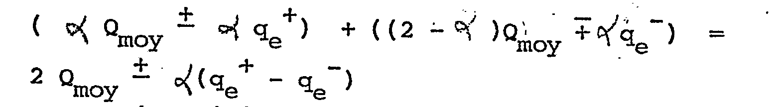
L'amplificateur différentiel selon l'invention a donc une réjection en mode commun dont l'efficacité ne dépend que de la précision avec laquelle peut être déterminée la capacité parasite Cp et donc le coefficient α.The differential amplifier according to the invention therefore has a rejection in common mode whose efficiency depends only on the precision with which the parasitic capacitance C p and therefore the coefficient α can be determined.
Claims (8)
Applications Claiming Priority (2)
| Application Number | Priority Date | Filing Date | Title |
|---|---|---|---|
| FR7914998 | 1979-06-12 | ||
| FR7914998A FR2458947A1 (en) | 1979-06-12 | 1979-06-12 | CHARGE TRANSFER PHASE INVERTER DEVICE AND DIFFERENTIAL AMPLIFIER COMPRISING SUCH A DEVICE |
Publications (2)
| Publication Number | Publication Date |
|---|---|
| EP0021908A1 true EP0021908A1 (en) | 1981-01-07 |
| EP0021908B1 EP0021908B1 (en) | 1983-06-29 |
Family
ID=9226484
Family Applications (1)
| Application Number | Title | Priority Date | Filing Date |
|---|---|---|---|
| EP80400786A Expired EP0021908B1 (en) | 1979-06-12 | 1980-06-03 | Charge transfer phase inverter and differential amplifier comprising such a device |
Country Status (5)
| Country | Link |
|---|---|
| US (1) | US4337403A (en) |
| EP (1) | EP0021908B1 (en) |
| JP (1) | JPS564907A (en) |
| DE (1) | DE3063959D1 (en) |
| FR (1) | FR2458947A1 (en) |
Cited By (1)
| Publication number | Priority date | Publication date | Assignee | Title |
|---|---|---|---|---|
| US11007573B2 (en) | 2009-01-15 | 2021-05-18 | David Kyle Pierce | Continuous, semicontinuous and batch methods for treating liquids and manufacturing certain constituents (e.g., nanoparticles) in liquids, apparatuses and nanoparticles and nanoparticle/liquid solution(s) and colloids resulting therefrom |
Families Citing this family (2)
| Publication number | Priority date | Publication date | Assignee | Title |
|---|---|---|---|---|
| JPS58202688A (en) * | 1982-05-21 | 1983-11-25 | Sony Corp | Color signal processing charge transfer device |
| US4509181A (en) * | 1982-05-28 | 1985-04-02 | Rca Corporation | CCD charge substraction arrangement |
Citations (3)
| Publication number | Priority date | Publication date | Assignee | Title |
|---|---|---|---|---|
| US3935477A (en) * | 1973-04-23 | 1976-01-27 | Bell Telephone Laboratories, Incorporated | Analog inverter for use in charge transfer apparatus |
| US4071775A (en) * | 1976-04-02 | 1978-01-31 | Texas Instruments Incorporated | Charge coupled differential amplifier for transversal filter |
| FR2365245A1 (en) * | 1976-09-15 | 1978-04-14 | Hughes Aircraft Co | SUBTRACTION CIRCUIT WITH LOAD COUPLING DEVICES |
Family Cites Families (3)
| Publication number | Priority date | Publication date | Assignee | Title |
|---|---|---|---|---|
| US4099197A (en) * | 1976-08-12 | 1978-07-04 | Northern Telecom Limited | Complementary input structure for charge coupled device |
| US4210825A (en) * | 1976-12-08 | 1980-07-01 | Bell Telephone Laboratories, Incorporated | Linear differential charge splitting input for charge coupled devices |
| FR2427009A1 (en) * | 1978-05-26 | 1979-12-21 | Thomson Csf | DIFFERENTIAL DEVICE USING THE TRANSFER OF ELECTRIC CHARGES IN A SEMICONDUCTOR, AND FILTER AND DELAY LINE CONTAINING SUCH A DEVICE |
-
1979
- 1979-06-12 FR FR7914998A patent/FR2458947A1/en active Granted
-
1980
- 1980-06-03 EP EP80400786A patent/EP0021908B1/en not_active Expired
- 1980-06-03 DE DE8080400786T patent/DE3063959D1/en not_active Expired
- 1980-06-11 JP JP7886380A patent/JPS564907A/en active Pending
- 1980-06-12 US US06/158,863 patent/US4337403A/en not_active Expired - Lifetime
Patent Citations (3)
| Publication number | Priority date | Publication date | Assignee | Title |
|---|---|---|---|---|
| US3935477A (en) * | 1973-04-23 | 1976-01-27 | Bell Telephone Laboratories, Incorporated | Analog inverter for use in charge transfer apparatus |
| US4071775A (en) * | 1976-04-02 | 1978-01-31 | Texas Instruments Incorporated | Charge coupled differential amplifier for transversal filter |
| FR2365245A1 (en) * | 1976-09-15 | 1978-04-14 | Hughes Aircraft Co | SUBTRACTION CIRCUIT WITH LOAD COUPLING DEVICES |
Non-Patent Citations (1)
| Title |
|---|
| IBM TECHNICAL DISCLOSURE BULLETIN, Vol. 18, No. 9, Fevrier 1976, New York, US D.L. CRITCHLOW et al. "Magnitude differencing circuit". pages 3071-3072. * Article en entier * * |
Cited By (1)
| Publication number | Priority date | Publication date | Assignee | Title |
|---|---|---|---|---|
| US11007573B2 (en) | 2009-01-15 | 2021-05-18 | David Kyle Pierce | Continuous, semicontinuous and batch methods for treating liquids and manufacturing certain constituents (e.g., nanoparticles) in liquids, apparatuses and nanoparticles and nanoparticle/liquid solution(s) and colloids resulting therefrom |
Also Published As
| Publication number | Publication date |
|---|---|
| EP0021908B1 (en) | 1983-06-29 |
| US4337403A (en) | 1982-06-29 |
| FR2458947B1 (en) | 1984-08-24 |
| FR2458947A1 (en) | 1981-01-02 |
| DE3063959D1 (en) | 1983-08-04 |
| JPS564907A (en) | 1981-01-19 |
Similar Documents
| Publication | Publication Date | Title |
|---|---|---|
| EP0030173B1 (en) | Switched capacitor charge transfer filter | |
| EP0237365A1 (en) | Photo-sensitive device | |
| EP0010014B1 (en) | Charge transfer filter and switched capacitor filter comprising a voltage muliplier having switched capacitors | |
| EP0168267A1 (en) | Multilinear charge tranfer array and scanning method | |
| EP0011556B1 (en) | Digitally programmable charge transfer filter | |
| EP0006053B1 (en) | Charge coupled differential device; filter and delay line comprising such a device | |
| EP1608069A2 (en) | Method for controling an analog switch | |
| EP0021908B1 (en) | Charge transfer phase inverter and differential amplifier comprising such a device | |
| EP0325524B1 (en) | Charge transfer memory and method of producing it | |
| EP0098191A1 (en) | Photosensor with anti-blooming control | |
| EP0182679B1 (en) | Line transfer photosensitive device with feed-back amplifiers | |
| EP0281465B1 (en) | Memory sense amplifier | |
| EP0604281B1 (en) | CCD shift register with improved read-out device | |
| EP0019506B1 (en) | Charge substraction and charge quantity generation transfer device | |
| EP0323924B1 (en) | Low-noise detection method and circuit for a photosensitive line transfer matrix | |
| FR2511545A1 (en) | SEMICONDUCTOR DEVICE COMPRISING A FOUR-PHASE CHARGE COUPLING DEVICE | |
| EP0012667B1 (en) | Method of filtering an electric signal by charge transfer in a semi-conductor and switched capacitor filter utilizing such a method | |
| EP0028961A1 (en) | Charge transfer filter and switched capacitor filter comprising a voltage multiplier with switched capacitors | |
| FR2561470A1 (en) | TRANSVERSE FILTER WITH CHARGE COUPLING | |
| FR2558670A1 (en) | IMPROVEMENT TO SOLID STATE PHOTOSENSITIVE DEVICES | |
| EP0645884B1 (en) | Current mode amplifier chain, operational amplifier, gain cell and corresponding amplifying elements | |
| EP0031751B1 (en) | Charge-transfer coded voltage generator, analog-digital coder and decoder comprising such a generator | |
| EP0017541B1 (en) | Transversal electric-charge transfer filter | |
| EP0334735B1 (en) | Device for reading electrical charges supplied by photodiodes with a semiconductor substrate | |
| FR2759509A1 (en) | INTEGRATED CIRCUIT WITH IMPROVED LINEARITY |
Legal Events
| Date | Code | Title | Description |
|---|---|---|---|
| PUAI | Public reference made under article 153(3) epc to a published international application that has entered the european phase |
Free format text: ORIGINAL CODE: 0009012 |
|
| AK | Designated contracting states |
Designated state(s): DE GB NL |
|
| 17P | Request for examination filed |
Effective date: 19810117 |
|
| GRAA | (expected) grant |
Free format text: ORIGINAL CODE: 0009210 |
|
| AK | Designated contracting states |
Designated state(s): DE GB NL |
|
| REF | Corresponds to: |
Ref document number: 3063959 Country of ref document: DE Date of ref document: 19830804 |
|
| PLBE | No opposition filed within time limit |
Free format text: ORIGINAL CODE: 0009261 |
|
| STAA | Information on the status of an ep patent application or granted ep patent |
Free format text: STATUS: NO OPPOSITION FILED WITHIN TIME LIMIT |
|
| 26N | No opposition filed | ||
| PGFP | Annual fee paid to national office [announced via postgrant information from national office to epo] |
Ref country code: GB Payment date: 19970521 Year of fee payment: 18 |
|
| PGFP | Annual fee paid to national office [announced via postgrant information from national office to epo] |
Ref country code: DE Payment date: 19970522 Year of fee payment: 18 |
|
| PGFP | Annual fee paid to national office [announced via postgrant information from national office to epo] |
Ref country code: NL Payment date: 19970616 Year of fee payment: 18 |
|
| PG25 | Lapsed in a contracting state [announced via postgrant information from national office to epo] |
Ref country code: GB Free format text: LAPSE BECAUSE OF NON-PAYMENT OF DUE FEES Effective date: 19980603 |
|
| PG25 | Lapsed in a contracting state [announced via postgrant information from national office to epo] |
Ref country code: NL Free format text: LAPSE BECAUSE OF NON-PAYMENT OF DUE FEES Effective date: 19990101 |
|
| GBPC | Gb: european patent ceased through non-payment of renewal fee |
Effective date: 19980603 |
|
| NLV4 | Nl: lapsed or anulled due to non-payment of the annual fee |
Effective date: 19990101 |
|
| PG25 | Lapsed in a contracting state [announced via postgrant information from national office to epo] |
Ref country code: DE Free format text: LAPSE BECAUSE OF NON-PAYMENT OF DUE FEES Effective date: 19990401 |