EP0021908A1 - Phasenumkehrschaltung mit Ladungsübertragung und Differenzverstärker mit solch einer Schaltung - Google Patents
Phasenumkehrschaltung mit Ladungsübertragung und Differenzverstärker mit solch einer Schaltung Download PDFInfo
- Publication number
- EP0021908A1 EP0021908A1 EP80400786A EP80400786A EP0021908A1 EP 0021908 A1 EP0021908 A1 EP 0021908A1 EP 80400786 A EP80400786 A EP 80400786A EP 80400786 A EP80400786 A EP 80400786A EP 0021908 A1 EP0021908 A1 EP 0021908A1
- Authority
- EP
- European Patent Office
- Prior art keywords
- voltage
- charges
- under
- electrode
- transfer
- Prior art date
- Legal status (The legal status is an assumption and is not a legal conclusion. Google has not performed a legal analysis and makes no representation as to the accuracy of the status listed.)
- Granted
Links
- 238000002347 injection Methods 0.000 claims description 18
- 239000007924 injection Substances 0.000 claims description 18
- 239000000758 substrate Substances 0.000 claims description 9
- 238000011144 upstream manufacturing Methods 0.000 claims description 6
- 239000004065 semiconductor Substances 0.000 claims description 3
- 238000012423 maintenance Methods 0.000 claims 1
- 238000010586 diagram Methods 0.000 description 7
- 238000006243 chemical reaction Methods 0.000 description 3
- 230000003071 parasitic effect Effects 0.000 description 3
- VYPSYNLAJGMNEJ-UHFFFAOYSA-N Silicium dioxide Chemical compound O=[Si]=O VYPSYNLAJGMNEJ-UHFFFAOYSA-N 0.000 description 1
- 240000008042 Zea mays Species 0.000 description 1
- 230000015572 biosynthetic process Effects 0.000 description 1
- 239000000969 carrier Substances 0.000 description 1
- 239000002800 charge carrier Substances 0.000 description 1
- 238000009792 diffusion process Methods 0.000 description 1
- 230000007717 exclusion Effects 0.000 description 1
- 238000002513 implantation Methods 0.000 description 1
- 239000012212 insulator Substances 0.000 description 1
- 230000010354 integration Effects 0.000 description 1
- 150000002500 ions Chemical class 0.000 description 1
- 238000002955 isolation Methods 0.000 description 1
- 244000045947 parasite Species 0.000 description 1
- 230000000737 periodic effect Effects 0.000 description 1
- 230000010287 polarization Effects 0.000 description 1
- 229910052710 silicon Inorganic materials 0.000 description 1
- 239000010703 silicon Substances 0.000 description 1
- 229910052814 silicon oxide Inorganic materials 0.000 description 1
Images
Classifications
-
- H—ELECTRICITY
- H03—ELECTRONIC CIRCUITRY
- H03H—IMPEDANCE NETWORKS, e.g. RESONANT CIRCUITS; RESONATORS
- H03H15/00—Transversal filters
-
- H—ELECTRICITY
- H03—ELECTRONIC CIRCUITRY
- H03F—AMPLIFIERS
- H03F3/00—Amplifiers with only discharge tubes or only semiconductor devices as amplifying elements
- H03F3/005—Amplifiers with only discharge tubes or only semiconductor devices as amplifying elements using switched capacitors, e.g. dynamic amplifiers; using switched capacitors as resistors in differential amplifiers
Definitions
- the present invention relates to a charge transfer phase reversing device.
- the signal to be inverted is generally converted into voltage, then the phase inversion is created into voltage and the voltage variations are re-injected into charges in the charge transfer device.
- the conversions of charges into voltage and vice versa have the disadvantage of being not very linear and of gain which is difficult to reproduce.
- the devices making it possible to carry out these conversions and the phase-to-voltage inversion are generally bulky and of high consumption.
- the present invention relates to a device which performs the phase inversion of a signal while remaining in the field of loads.
- This device has the advantage of being easily integrated into a more complex charge transfer device. It allows to obtain with good precision two signals in phase opposition. In a preferred embodiment, this device does not require, in addition to the DC input voltage which is applied to several transfer electrodes and storage, only three clock signals which ensure the transfer of charges, which increases its simplicity and precision.
- the device according to the invention makes it possible in particular to produce a differential amplifier which does not require conversion of the charges into voltage and which therefore has, compared with the differential amplifiers according to known art, advantages from the point of view of consumption and integration.
- the present invention relates to a charge transfer phase reversing device which receives an input voltage V e constituted by the superposition of a direct voltage V o and a time-varying and sampled voltage v e and which comprises means making the difference between the quantity of charges double that corresponding to the direct voltage V o and the quantity of charges corresponding to each sample of the variable voltage V e superimposed on the direct voltage.
- V e an input voltage
- V o constituted by the superposition of a direct voltage V o and a time-varying and sampled voltage v e
- V e V o ⁇ V e .
- Q e Q avg ⁇ q e .
- the device according to the invention therefore allows to obtain, from a quantity of charges Q avg + q e , a quantity of charges Q avg - qe and vice versa. A phase inversion on the charges is therefore carried out.
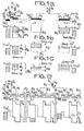
- Figure 1a shows a cross-sectional view of an embodiment of the device according to the invention.
- the device according to the invention is produced on a semiconductor substrate 1, of type P silicon in the example, covered with an insulating layer, of silicon oxide in the example, which is not shown in the Figure 1a. On this insulating layer, alternate charge storage and transfer electrodes which are arranged substantially normally in the direction of charge propagation. The transfer electrodes are deposited on an insulating thickness which is not shown in FIG. 1a.
- this arrangement has a double function, on the one hand ensuring the continuity of the potentials created in the semiconductor 1, and on the other hand imposing a single transfer direction for the charge carriers.
- This structure comprising an extra thickness of insulator can be replaced by an overdoping of the substrate, by implantation of ions, ensuring the same functions.
- FIG. 1a only the transfer and storage electrodes constituting the phase reversing device according to the invention have been shown, with the exclusion of the transfer and storage electrodes ensuring only the transfer of the charges.
- the means performing the subtraction include in particular a first and a second storage electrodes G1 and G 2 electrically connected at a point P which can be connected to the voltage continuous V 0 or which can be left floating, i.e. not connected to any voltage source.
- a switch K symbolically represents the two possibilities of polarization of point P.
- a transfer electrode G o1 Upstream of the first storage electrode, in the direction of charge transfer indicated by an arrow, is a transfer electrode G o1 , brought to a constant voltage V T , and a charge injection diode D e1 , connected at a variable voltage V D.
- the point P is connected to the constant voltage V o .
- the voltage V D applied to the diode D e1 is successively lower then greater than the surface potential V ref under the transfer electrode G o1 connected to V T.
- a quantity of reference charges Q ref is thus stored under the storage electrode G 1 .
- the phase reversing device further comprises a third storage electrode G e located upstream of the second, G 2 , in the direction of charge transfer indicated by an arrow.
- This third storage electrode G e receives the input voltage V e at a point O. Between the point O and a point N, is connected a resistance R. Between the point O and a point M, is connected a capacitance C. The DC input voltage V o is applied to the point N and the voltage variable in time and sampled V e is applied to point M.
- a transfer electrode G Oe carried, as G o1 , at constant voltage V T and a charge injection diode D e2 , carried as D e1 , at the variable voltage V D.
- FIGs 1a, b, c there are shown diagrams illustrating the operation of the device according to the invention. These diagrams represent the evolution of the surface potential ⁇ s in the substrate 1. The hatched areas indicate the presence of minority carriers.
- FIG. 1a illustrates the injection of a quantity of charges Q ref under the electrode G 1 and a quantity of charges Q under the electrode G.
- the injection of charges under the electrodes G 1 and G 2 is done in the same way.
- the transfer electrodes G o1 and G oe are connected to the constant voltage V T which fixes the surface potential under G 1 and G e at the maximum value V ref .
- the voltage V D applied to the diodes D e1 and D e2 successively takes a value lower then higher than the surface potential V ref , which causes the storage of the quantities of charges Q ref and Q e under G 1 and G e .
- the quantity of charges stored under G 1 , Q ref must be equal to twice the quantity of charges Q avg corresponding to the DC input voltage V o .
- the quantity of charges Q injected under the electrode G e which receives the voltage V V o ⁇ v e is written: is a constant which depends on V ref and on physical characteristics which are the same for the whole of the charge transfer device on which the inverter is made and where C e represents the oxide capacity of the electrode G e .
- the quantity of charges Q avg therefore equals (V o - V a ) C e .
- the storage electrode G 1 is generally given a surface twice that of G e , which can be achieved with good precision.
- V T the constant voltage applied to the transfer electrodes G o1 and G Oe , equal to the DC input voltage V o .
- FIG. 1a represents the surface potentials under the device according to the invention in the case where V equals V o and in the case where the surface of the electrode G 1 is twice that of the electrode G e .
- the input voltage V e can vary around V o between Va and 2 V o - Va.
- the surface potential under Geav before the charge injection can therefore vary by the same amount ⁇ 0 around ⁇ o .
- the variation in surface potential ⁇ under the second storage electrode G 2 depends, for a given quantity of charges Q e , on the relative values of the oxide capacities C 1 and C 2 of the storage electrodes G 1 and G 2 .
- the potential well created under the second storage electrode G 2 must be sufficient for the maximum quantity of charges Q max , injected under G e and corresponding to a well depth under Ge before injection of charges equal to ⁇ o + ⁇ ⁇ o , can be stored there.
- the oxide capacity of G 2 (and therefore the surface of G 2 ) is chosen such that:
- FIGS. 1a, b, c represent the surface potentials in the substrate in the case where:
- the variations in surface potential under G 2 , ⁇ are equal to the variations in surface potential under G e , ⁇ ⁇ e .
- FIG. 1b represents the surface potentials in the case where the quantity of charges injected Q e equals:
- FIG. 1c represents the surface potentials in the substrate in the case where
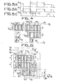
- FIG. 2 shows a cross-sectional view showing the device shown in Figure 1a inserted in a more complex load transfer device, as well as a diagram illustrating the transfer of loads.
- pairs of transfer electrode G o - storage electrode G which ensure the transfer of the charges, are added to the device according to the invention represented in FIG. 1a between the grids G e and G 2 , after the electrode G 2 and after electrode G 1 .
- the transfer electrode G 02 which precedes G 2 is brought to a constant voltage Vu less than V o to increase the depth of the well under G2.
- FIGS. 3a, b, c represent diagrams of signals which can be applied to the device shown in FIG. 2.
- These clock signals ⁇ 1 , ⁇ 2 and ⁇ 3 are periodic functions of the same period T, the amplitude of which varies between a low level and a high level.
- the signals ⁇ 1 and ⁇ 2 are practically in phase opposition, with however a slight overlap at the high level as is customary in the field of charge transfers.
- the signal ⁇ 3 goes high while ⁇ 1 is already there and returns to the low level before ⁇ 1 .
- the signal ⁇ 1 is applied to the diodes D e1 and D e2 , as well as to a transfer electrode-storage electrode pair out of two, and in particular to that which follows the electrode G e .
- the signal ⁇ 2 is applied to the MOS transistor T 1 , connected between the point P and the voltage V o , and which replaces the switch K shown in FIG. 1a.
- the ⁇ 2 signal is also applied to a torque transfer electrode - on two storage electrode, and in particular to that which precedes the torque transfer electrode G02 - storage electrode G 2.
- the signal ⁇ 3 is applied to the pair of electrodes following the storage electrodes G 1 and G2.
- the signal ⁇ 2 is at the high level and the signals ⁇ 1 and ⁇ 3 are at the low level.
- the surface potentials in the substrate are shown in Figure 2 in solid lines.
- the electrodes G 1 and G 2 receive by the transistor T 1 which is made conductive the direct voltage V o .
- the passage from ⁇ 1 to the low level causes the diodes to inject the quantities of charges Q ref and Q e under G 1 and Ge These quantities of charges are blocked under G 1 and G e by the pairs of electrodes along G 1 and G e which are at the low level.
- the signal ⁇ 1 is at the high level and the signals ⁇ 2 and ⁇ 3 are at the low level.
- the potentials in the substrate are shown in broken lines in FIG. 2.
- the pair of electrodes preceding the pair of transfer electrode G o2 - storage electrode G 2 ensures the transfer under G 2 of the quantity of charges Q e , and thus the formation of the quantity of charges Q avg Q e , corresponding to the signal reversed in phase under the electrode G 1 .
- the signals ⁇ 1 and ⁇ 3 are at the high level and the signal ⁇ 2 is at the low level.
- the surface potentials in the substrate are shown in dotted lines in FIG. 2.
- the pairs of electrodes along G 1 and G 2 which are brought to the high level, ensure the evacuation of the charges stored under G 1 and under G 2 .
- the device according to the invention is thus ready to receive at time t 1 according to a new quantity of charges Q e corresponding to a sample of the input voltage under the electrode G. e
- FIG. 4 represents a top view of a device similar to that of FIG. 2.
- the storage electrodes G e and G 2 on the one hand, and G 1 on the other hand, are produced in two parallel charge transfer channels 2 and 3.
- the channel 2 delivers charge quantities corresponding to the input voltage V e and channel 3 delivers quantities of charges corresponding to the input voltage reversed in phase.
- the device shown in FIG. 4 has the advantage, from the point of view of practical implementation, of having a reduced bulk.
- FIG. 5 represents a top view of a differential amplifier according to the invention.
- the device shown in FIG. 5 includes a phase reversing device as previously described, which reverses the phase of one of the two input voltages of the differential amplifier, ie V e this voltage.
- the differential amplifier according to the invention comprises several charge transfer channels isolated by isolation and parallel diffusions. It notably includes channels 2 and 3 identical to those shown in FIG. 4. Channel 2 receives the input voltage to be inverted V and transfers the charge to be inverted Q e . Channel 3 generates the reverse signal load - Q and transfers it.
- the differential amplifier according to the invention also comprises a channel 4 which receives the second input voltage from the differential amplifier V e + and which transfers the charge Q e + .
- a channel 5 joins channels 3 and 4 and adds the charges Q e + and - Q e - . These charges are transferred to channel 5 and read on floating diodes D 1 and D 2 . connected to a follower stage, as is known.
- Channel 4 includes a charge injection device identical to that of channel 2. This device consists in particular of a charge injection diode D e3 and a storage electrode G ' e to which the input voltage V e + of the differential amplifier.
- phase reversing device depends above all on the parasitic capacitance Cp existing at point P where the first and second storage electrodes G 1 and G 2 are connected.
- the parasitic capacitance Cp means that the quantity of charges which is removed from G 2 when Q e arrives - under G 1 is not equal to Q e - but to ⁇ Q e - which is defined:
- the quantity of initial charges Q initial under G 1 is equal to 2 Q avg .
- the quantity of final charges Q under G 1 is therefore expressed:
- the final quantity of charges under the electrode G 1 therefore consists of a constant term (2- ⁇ ) Q avg and a variable term + ⁇ q e -.
- the error in g entered by the coefficient ⁇ on the variable term can be compensated for by injecting the quantity of charges Q + on channel 4 with an attenuation factor ⁇
- the differential amplifier according to the invention therefore has a rejection in common mode whose efficiency depends only on the precision with which the parasitic capacitance C p and therefore the coefficient ⁇ can be determined.
Landscapes
- Engineering & Computer Science (AREA)
- Power Engineering (AREA)
- Solid State Image Pick-Up Elements (AREA)
- Amplifiers (AREA)
Applications Claiming Priority (2)
| Application Number | Priority Date | Filing Date | Title |
|---|---|---|---|
| FR7914998A FR2458947A1 (fr) | 1979-06-12 | 1979-06-12 | Dispositif inverseur de phase a transfert de charges et amplificateur differentiel comportant un tel dispositif |
| FR7914998 | 1979-06-12 |
Publications (2)
| Publication Number | Publication Date |
|---|---|
| EP0021908A1 true EP0021908A1 (de) | 1981-01-07 |
| EP0021908B1 EP0021908B1 (de) | 1983-06-29 |
Family
ID=9226484
Family Applications (1)
| Application Number | Title | Priority Date | Filing Date |
|---|---|---|---|
| EP80400786A Expired EP0021908B1 (de) | 1979-06-12 | 1980-06-03 | Phasenumkehrschaltung mit Ladungsübertragung und Differenzverstärker mit solch einer Schaltung |
Country Status (5)
| Country | Link |
|---|---|
| US (1) | US4337403A (de) |
| EP (1) | EP0021908B1 (de) |
| JP (1) | JPS564907A (de) |
| DE (1) | DE3063959D1 (de) |
| FR (1) | FR2458947A1 (de) |
Cited By (1)
| Publication number | Priority date | Publication date | Assignee | Title |
|---|---|---|---|---|
| US11007573B2 (en) | 2009-01-15 | 2021-05-18 | David Kyle Pierce | Continuous, semicontinuous and batch methods for treating liquids and manufacturing certain constituents (e.g., nanoparticles) in liquids, apparatuses and nanoparticles and nanoparticle/liquid solution(s) and colloids resulting therefrom |
Families Citing this family (2)
| Publication number | Priority date | Publication date | Assignee | Title |
|---|---|---|---|---|
| JPS58202688A (ja) * | 1982-05-21 | 1983-11-25 | Sony Corp | 色信号処理用電荷転送装置 |
| US4509181A (en) * | 1982-05-28 | 1985-04-02 | Rca Corporation | CCD charge substraction arrangement |
Citations (3)
| Publication number | Priority date | Publication date | Assignee | Title |
|---|---|---|---|---|
| US3935477A (en) * | 1973-04-23 | 1976-01-27 | Bell Telephone Laboratories, Incorporated | Analog inverter for use in charge transfer apparatus |
| US4071775A (en) * | 1976-04-02 | 1978-01-31 | Texas Instruments Incorporated | Charge coupled differential amplifier for transversal filter |
| FR2365245A1 (fr) * | 1976-09-15 | 1978-04-14 | Hughes Aircraft Co | Circuit de soustraction a dispositifs a couplage par charges |
Family Cites Families (3)
| Publication number | Priority date | Publication date | Assignee | Title |
|---|---|---|---|---|
| US4099197A (en) * | 1976-08-12 | 1978-07-04 | Northern Telecom Limited | Complementary input structure for charge coupled device |
| US4210825A (en) * | 1976-12-08 | 1980-07-01 | Bell Telephone Laboratories, Incorporated | Linear differential charge splitting input for charge coupled devices |
| FR2427009A1 (fr) * | 1978-05-26 | 1979-12-21 | Thomson Csf | Dispositif differentiel utilisant le transfert de charges electriques dans un semi-conducteur, et filtre et ligne a retard comportant un tel dispositif |
-
1979
- 1979-06-12 FR FR7914998A patent/FR2458947A1/fr active Granted
-
1980
- 1980-06-03 DE DE8080400786T patent/DE3063959D1/de not_active Expired
- 1980-06-03 EP EP80400786A patent/EP0021908B1/de not_active Expired
- 1980-06-11 JP JP7886380A patent/JPS564907A/ja active Pending
- 1980-06-12 US US06/158,863 patent/US4337403A/en not_active Expired - Lifetime
Patent Citations (3)
| Publication number | Priority date | Publication date | Assignee | Title |
|---|---|---|---|---|
| US3935477A (en) * | 1973-04-23 | 1976-01-27 | Bell Telephone Laboratories, Incorporated | Analog inverter for use in charge transfer apparatus |
| US4071775A (en) * | 1976-04-02 | 1978-01-31 | Texas Instruments Incorporated | Charge coupled differential amplifier for transversal filter |
| FR2365245A1 (fr) * | 1976-09-15 | 1978-04-14 | Hughes Aircraft Co | Circuit de soustraction a dispositifs a couplage par charges |
Non-Patent Citations (1)
| Title |
|---|
| IBM TECHNICAL DISCLOSURE BULLETIN, Vol. 18, No. 9, Fevrier 1976, New York, US D.L. CRITCHLOW et al. "Magnitude differencing circuit". pages 3071-3072. * Article en entier * * |
Cited By (1)
| Publication number | Priority date | Publication date | Assignee | Title |
|---|---|---|---|---|
| US11007573B2 (en) | 2009-01-15 | 2021-05-18 | David Kyle Pierce | Continuous, semicontinuous and batch methods for treating liquids and manufacturing certain constituents (e.g., nanoparticles) in liquids, apparatuses and nanoparticles and nanoparticle/liquid solution(s) and colloids resulting therefrom |
Also Published As
| Publication number | Publication date |
|---|---|
| DE3063959D1 (en) | 1983-08-04 |
| EP0021908B1 (de) | 1983-06-29 |
| US4337403A (en) | 1982-06-29 |
| FR2458947A1 (fr) | 1981-01-02 |
| JPS564907A (en) | 1981-01-19 |
| FR2458947B1 (de) | 1984-08-24 |
Similar Documents
| Publication | Publication Date | Title |
|---|---|---|
| EP0030173B1 (de) | Ladungsverschiebungsfilter mit geschalteten Kapazitäten | |
| EP0237365A1 (de) | Lichtempfindliche Vorrichtung | |
| EP0010014B1 (de) | Filter mit Ladungsverschiebung und Filter mit Kapazitätsumschaltung, jeweils mit einem auf Kapazitätsumschaltung beruhenden Spannungsvervielfacher | |
| EP0168267A1 (de) | Aus mehreren Zeilen bestehende ladungsgekoppelte Sensoranordnung und Abtastverfahren | |
| EP0011556B1 (de) | Numerisch programmierbares Ladungsübertragungsfilter | |
| EP0006053B1 (de) | Differenzbildungsvorrichtung mit Ladungskopplung; Filter und Verzögerungsleitung mit einer solchen Vorrichtung | |
| EP1608069A2 (de) | Verfahren zur Steuerung eines Analogschalters | |
| EP0021908B1 (de) | Phasenumkehrschaltung mit Ladungsübertragung und Differenzverstärker mit solch einer Schaltung | |
| EP0325524B1 (de) | Ladungstransferspeicher und Verfahren zur Herstellung desselben | |
| EP0098191A1 (de) | Optoelektronischer Sensor mit Überlaufvorrichtung | |
| EP0182679B1 (de) | Photoempfindliche Zwischenspaltanordnung mit zurückgekoppeltem Verstärker | |
| EP0281465B1 (de) | Speicherleseverstärker | |
| EP0019506B1 (de) | Ladungsverschiebevorrichtung für Ladungssubstraktion und Ladungserzeugung | |
| EP0323924B1 (de) | Leseverfahren und Schaltung mit niedrigem Geräusch für photosensitive Zeilentransfermatrix | |
| FR2511545A1 (fr) | Dispositif semi-conducteur comportant un dispositif a couplage de charges a quatre phases | |
| EP0012667B1 (de) | Verfahren zum Filtern eines elektrischen Signals durch Ladungsübertragung in einem Halbleiter und Filter mit geschalteten Kondensatoren, das dieses Verfahren verwendet | |
| EP0958545B1 (de) | Integratorschaltung von photoerzeugten ladungen mit verbesserter linearität | |
| EP0028961A1 (de) | Ladungsverschiebungsfilter und Filter mit geschalteten Kapazitäten versehen mit einem Vervielfacher mit geschalteten Kapazitäten | |
| FR2561470A1 (fr) | Filtre transversal a couplage de charges | |
| FR2558670A1 (fr) | Perfectionnement aux dispositifs photosensibles a l'etat solide | |
| EP0645884B1 (de) | Verstärkerkette in Strommode, Operationsverstärker, Verstärkungszelle und zugehöriges Verstärkerelement | |
| EP0031751B1 (de) | Ladungstransportgenerator kodierter Spannung; mit solchem Ladungstransportgenerator ausgerüsteter Analog-Digital-Kodierer und -Dekodierer | |
| EP0017541B1 (de) | Transversal-Filter mit elektrischer Ladungsverschiebung | |
| EP0334735B1 (de) | Einrichtung zum Auslesen von elektrischen Ladungen, die durch Halbleitersubstrat-Photodioden geliefert werden | |
| EP0322303A1 (de) | Ladungsverschiebeanordnung mit Senkung der Ausgangsverschiebespannung und Verfahren zu ihrer Herstellung |
Legal Events
| Date | Code | Title | Description |
|---|---|---|---|
| PUAI | Public reference made under article 153(3) epc to a published international application that has entered the european phase |
Free format text: ORIGINAL CODE: 0009012 |
|
| AK | Designated contracting states |
Designated state(s): DE GB NL |
|
| 17P | Request for examination filed |
Effective date: 19810117 |
|
| GRAA | (expected) grant |
Free format text: ORIGINAL CODE: 0009210 |
|
| AK | Designated contracting states |
Designated state(s): DE GB NL |
|
| REF | Corresponds to: |
Ref document number: 3063959 Country of ref document: DE Date of ref document: 19830804 |
|
| PLBE | No opposition filed within time limit |
Free format text: ORIGINAL CODE: 0009261 |
|
| STAA | Information on the status of an ep patent application or granted ep patent |
Free format text: STATUS: NO OPPOSITION FILED WITHIN TIME LIMIT |
|
| 26N | No opposition filed | ||
| PGFP | Annual fee paid to national office [announced via postgrant information from national office to epo] |
Ref country code: GB Payment date: 19970521 Year of fee payment: 18 |
|
| PGFP | Annual fee paid to national office [announced via postgrant information from national office to epo] |
Ref country code: DE Payment date: 19970522 Year of fee payment: 18 |
|
| PGFP | Annual fee paid to national office [announced via postgrant information from national office to epo] |
Ref country code: NL Payment date: 19970616 Year of fee payment: 18 |
|
| PG25 | Lapsed in a contracting state [announced via postgrant information from national office to epo] |
Ref country code: GB Free format text: LAPSE BECAUSE OF NON-PAYMENT OF DUE FEES Effective date: 19980603 |
|
| PG25 | Lapsed in a contracting state [announced via postgrant information from national office to epo] |
Ref country code: NL Free format text: LAPSE BECAUSE OF NON-PAYMENT OF DUE FEES Effective date: 19990101 |
|
| GBPC | Gb: european patent ceased through non-payment of renewal fee |
Effective date: 19980603 |
|
| NLV4 | Nl: lapsed or anulled due to non-payment of the annual fee |
Effective date: 19990101 |
|
| PG25 | Lapsed in a contracting state [announced via postgrant information from national office to epo] |
Ref country code: DE Free format text: LAPSE BECAUSE OF NON-PAYMENT OF DUE FEES Effective date: 19990401 |