EP0021697B1 - Electrode probe - Google Patents
Electrode probe Download PDFInfo
- Publication number
- EP0021697B1 EP0021697B1 EP80301932A EP80301932A EP0021697B1 EP 0021697 B1 EP0021697 B1 EP 0021697B1 EP 80301932 A EP80301932 A EP 80301932A EP 80301932 A EP80301932 A EP 80301932A EP 0021697 B1 EP0021697 B1 EP 0021697B1
- Authority
- EP
- European Patent Office
- Prior art keywords
- electrode assembly
- electrode
- tip portion
- segments
- forward tip
- Prior art date
- Legal status (The legal status is an assumption and is not a legal conclusion. Google has not performed a legal analysis and makes no representation as to the accuracy of the status listed.)
- Expired
Links
- 239000000523 sample Substances 0.000 title claims description 52
- 238000010276 construction Methods 0.000 claims description 4
- 238000000576 coating method Methods 0.000 claims description 2
- 239000011248 coating agent Substances 0.000 claims 1
- 230000000284 resting effect Effects 0.000 claims 1
- 238000002347 injection Methods 0.000 description 42
- 239000007924 injection Substances 0.000 description 42
- 238000005259 measurement Methods 0.000 description 7
- 238000000034 method Methods 0.000 description 4
- 238000007747 plating Methods 0.000 description 4
- 230000000712 assembly Effects 0.000 description 3
- 238000000429 assembly Methods 0.000 description 3
- 239000004020 conductor Substances 0.000 description 2
- 239000011810 insulating material Substances 0.000 description 2
- 239000000463 material Substances 0.000 description 2
- 229910001220 stainless steel Inorganic materials 0.000 description 2
- 239000010935 stainless steel Substances 0.000 description 2
- 235000001674 Agaricus brunnescens Nutrition 0.000 description 1
- 229910001369 Brass Inorganic materials 0.000 description 1
- 229920004943 Delrin® Polymers 0.000 description 1
- 239000004677 Nylon Substances 0.000 description 1
- 239000004809 Teflon Substances 0.000 description 1
- 229920006362 Teflon® Polymers 0.000 description 1
- 239000010951 brass Substances 0.000 description 1
- 238000010292 electrical insulation Methods 0.000 description 1
- 238000005516 engineering process Methods 0.000 description 1
- 238000000691 measurement method Methods 0.000 description 1
- 229920001778 nylon Polymers 0.000 description 1
Images

Classifications
-
- G—PHYSICS
- G01—MEASURING; TESTING
- G01R—MEASURING ELECTRIC VARIABLES; MEASURING MAGNETIC VARIABLES
- G01R1/00—Details of instruments or arrangements of the types included in groups G01R5/00 - G01R13/00 and G01R31/00
- G01R1/02—General constructional details
- G01R1/06—Measuring leads; Measuring probes
- G01R1/067—Measuring probes
- G01R1/06788—Hand-held or hand-manipulated probes, e.g. for oscilloscopes or for portable test instruments
Definitions
- This invention relates to instruments for measuring the conductivity of thin layers or coatings of electrically conductive material within apertures or holes and particularly to instruments for measuring the plating thickness or conductivity of electrically conductive material on the walls defining a through hole in printed circuit boards.
- Two pairs of electrodes, one pair on each side of the through hole are used for measuring the conductivity of plated through holes.
- One electrode of each pair is used for injecting current into the through hole and the other electrode of each pair is used for measuring the resulting voltage drop across the through hole.
- This technique is old in the art and is commonly referred to as the Kelvin technique or four-point measurement technique.
- the present invention overcomes the disadvantages of known instruments for measuring the thickness of through hole platings in circuit board workpieces by providing apparatus for injecting current substantially a full 360° into the through hole and also incorporating a voltage electrode for making multiple contacts with the through hole to insure a good electrical contact between the voltage electrode and the walls of the through hole.
- the electrode probe according to this invention comprises a first electrode assembly having a forward tip portion shaped to engage substantially 360° of a circular edge formed by the intersection of the wall defining the through hole and the surface of the circuit board workpiece; a second electrode assembly electrically insulated from said first electrode assembly and having a forward tip portion disposed adjacent the tip portion of the first electrode assembly and shaped to engage said circular edge when the forward tip portion of the first electrode assembly is positioned to engage the circular edge; characterised in that said first electrode assembly is of segmented construction having an interstice between adjacent segments thereof and said second electrode assembly is displaceably mounted within said interstice and its forward tip portion is shaped to contact said circular edge at at least two discrete and separated locations when the forward tip portion of said first electrode assembly is disposed in operative engagement with substantially 360° of said circular edge.
- the invention refers also to the use of the electrode probe as shown in claim 11.
- the current injection segments are spring biased in the forward direction but are movable against the spring bias to a rearward position.
- the current injection segments are brought into engagement with the circular edge of the through hole and are moved against the spring bias into the housing until each segment thereof is stopped by a stop means.
- the voltage electrode With the current electrode extended to its most forward position, the voltage electrode is recessed behind the forward tips of the current injection segments. When the current injection segments engage the through hole and are pushed rearwardly against the spring, the voltage tip is exposed.
- a hand held probe assembly 20 having a forward housing portion 22, having ribs 24 to provide for easy gripping by the user.
- a barrel cap or rearward housing portion 26 has a forward portion receiving the rearward portion of forward housing 22 and is affixed thereto by means of set screw 28 as shown in Fig. 2.
- a mushroom cap 30 preferably of a nylon type material such as sold under the trademark Delrin is frictionally mounted to the rearward end of the barrel cap 26.
- the forward housing portion 22 has a forward bore 32 extending axially and partially through the forward housing portion 22.
- the bore 32 is open at the forward end and closed at the rearward end.
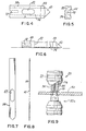
- Two current injection segments 34 and 36 for injecting current into a through hole are mounted in bore 32. These segments are of identical construction and one such segment is depicted in Figs. 4, 5 and 6.
- Each segment has a rearward portion 38 having a semi-circular cross-section as shown in Fig. 5 and having a forward rectangular block 39 which has its forward end shaped to form, preferably but by way of illustration only, a cone half 40 as shown in Figs. 4, 5 and 6.
- This cone half 40 is a forward tip portion of the current injection segments for engaging the through hole.
- the two current injection segments are made preferably of stainless steel. Before mounting in the housing of probe assembly 20, the two current injection segments are positioned with the flat sides of the rearward portions 38 adjacent to one another. A current injection electrode is thus provided having a rearward portion which has a cylindrical cross-section and which is mounted in the bore 32.
- Each of the current injection segments has a slot 42 as shown in Figs. 4, 5 and 6 through which an electrically non-conductive pin 48 is inserted after the current injection segments 34 and 36 are positioned inside bore 32.
- This pin 48 extends through bores 46 extending through opposite sides of the forward housing portion 22 and through the slots 42.
- the pin 48 is adhesively or press fit mounted in bore 46 and serves to hold the two current injection segments 34 and 36 in the bore 32.
- a spring 50 is compressively positioned between the rearward ends of the current injection segments 34 and 36 and the closed end of bore 32.
- the spring 50 biases the current injection segments in a forward position.
- Pin 48 acting against rearward edge 42a of slot 42 acts as a stop means for limiting or stopping the forward movement of the current injection segments 34 and 36.
- the forward edge 42b of the slot 42 which rests against the pin 48 when the current injection segments are moved in the rearward direction also acts as a stop means for limiting or stopping the rearward movement of the current injection segments.
- Rearward movement of current injection segments 34, and 36 may also be limited by the corner portions of the rearward face of rectangular block 39 striking the forward edge of forward housing 22 as shown in Fig. 3. Either stop means may be used to limit this rearward movement of current injection segments 34 and 36 and both are considered to be within the scope of the present invention.
- Each current injection segment also has a longitudinal channel 54 as shown in Figs. 4, 5 and 6.
- a voltage electrode spear 56 also preferably made of stainless steel and having a rectangular cross-section is positioned in the space bounded by the sides of the channel 54 as shown in Fig. 3.
- the voltage electrode spear 56 is shown in Figs. 7 and 8.
- the voltage spear 56 also has a slot 62 as shown in Fig. 7 through which the pin 48 extends to hold the voltage spear in the housing as shown in Fig. 2.
- the rearward edge of slot 62 provides a limit on the forward movement of the voltage spear 56 and the forward edge of slot 62 limits the rearward movement of voltage spear 56.
- the rearward portion of the voltage spear 56 is inserted in a slot 58 formed in an electrode holder 60 and soldered thereto.
- a rod like element 64 is soldered to the electrode holder 60 which has an enlarged diameter portion 66 which is mounted in a spring probe housing 68.
- a spring 70 is mounted compressively in the spring probe housing 68 between the rearward end of enlarged diameter portion 66 and a rearward closed end of spring probe housing 68. This spring 70 biases the rod 64 and thus the voltage spear 56 in a forward direction.
- the shoulder formed at the enlarged portion 66 on rod 64 engages a forward bent-in portion of housing 68 to retain the enlarged portion 66 and spring 70 in the spring probe housing 68.
- the forward movement of the voltage spear 56 is limited so that when the current injection segments 34 and 36 do not engage a through hole, the voltage spear is slightly recessed from the forward tips of the current injection segments 34 and 36.
- the current injection segments 34 and 36 serve to protect the voltage spear 56 from damage when the probe assembly is not being useful.
- each of the current injection segments 34 and 36 there is provided a bore 72 as shown in Figs. 4, 5 and 6.
- current posts 76 and 78 are mounted in the bores 72.
- Current posts 76 and 78 are preferably constructed of brass and soldered to the respective current injection segment.
- the current posts 76 and 78 slidably extend through bores 80 and 82 respectively in the rearward end of forward housing portion 22.
- the spring probe housing 68 is mounted in a bore 69 and is held in place by a pressure-fit provided by an annular bulge 71 on spring probe housing 68 which depresses the wall of bore 69 at 73 as shown in Fig. 2.
- each of the current injection segments 34 and 36 is coated with an insulating material 55 such as material marketed under the trademark Teflon. This insulating material provides electrical insulation between the current injection segments 34 and 36 and the voltage spear 56 as shown in Figs. 2 and 3.
- probe unit 20 In order to make a measurement of electrical conductivity or resistivity of a plated through hole, two probe units must be used, one located on each side of the through hole of a circuit board workpiece as shown in Fig. 9. This is the arrangement for using the Kelvin or four-point technique of measuring conductivity or resistivity of a through hole.
- the probe 20 may be used in conjunction with another similar probe 20a as shown in Fig. 9.
- the probe units 20 and 20a are positioned axially with a plated through hole 88 in a circuit board 90. In discussing the operation of this probe unit, only probe unit 20 will be discussed. Probe 20a operates in a similar manner.
- the probe unit 20 is pushed by the user into the through hole 88 until the current injection segments 34 and 36 are moved to their most rearward position.
- the voltage electrode spear 56 normally recessed behind the forward tip of the current injection segments 34 and 36 prior to the time the current injection segments engage the through hole 88, becomes exposed when these segments move rearwardly with respect to the forward housing 22 against the biasing force of spring 50 as shown in Fig. 2.
- the voltage spear 56 then engages the circular edge of the through hole 88 on opposite sides of the through hole. Since the voltage electrode spear 56 engages the through hole at two places better electrical contact is insured than with the conventional one place contact.
- each of the current injection segments 34 and 36 are independently movable, errors caused by imperfections and discontinuities in the circular edge are reduced and superior current injection in approximately 360° of the through hole is achieved. Furthermore, the construction of probe 20 with the independently movable current injection segments allows a user a certain amount of flexibility in axially positioning the probe with the through hole. Therefore the probe need not be perfectly aligned perpendicular to the circuit board workpiece.
- the current leads 84 and 86 and the voltage lead 90 of probe 20 and the corresponding leads of probe 20a are directed to a readout unit or meter (not shown) which supplies current to the current injection segments of one probe unit and a current return path through the current injection segments of the other probe.
- the voltage measurement is made across the through hole between the voltage electrode spears of the two probes and is directed via the voltage leads 90 to the readout unit.
- the readout unit coverts the voltage measurement into utilizable intelligence such as the conductivity or resistivity of the through hole.
- a readout device which may be used, for example, is the CAVIDERM Model CD-6 manufactured by UPA Technology, Inc.
Landscapes
- Physics & Mathematics (AREA)
- General Physics & Mathematics (AREA)
- Measuring Leads Or Probes (AREA)
Description
- This invention relates to instruments for measuring the conductivity of thin layers or coatings of electrically conductive material within apertures or holes and particularly to instruments for measuring the plating thickness or conductivity of electrically conductive material on the walls defining a through hole in printed circuit boards.
- Two pairs of electrodes, one pair on each side of the through hole are used for measuring the conductivity of plated through holes. One electrode of each pair is used for injecting current into the through hole and the other electrode of each pair is used for measuring the resulting voltage drop across the through hole. This technique is old in the art and is commonly referred to as the Kelvin technique or four-point measurement technique.
- Electrical probe assemblies of various configurations are known such as described in U.S. Patent No. 902,753; U.S. Patent No. 2,142,619; U.S. Patent No. 2,208,023; U.S. Patent No. 2,437,697; U.S. Patent No. 3,042,862; U.S. Patent No. 3,192,474; U.S. Patent No. 3,335,358; U.S. Patent No. 3,676,776; British Patent Specification No. 922,225; W. Gee et al. A Versatile Over-Under Four-Point Probe Apparatus, J. Physics E. (GB), January, 1971, pp. 70-72; and R. M. Murcko, Split-Tip for Terminal Resistance Measurements, IBM Technical Disclosure Bulletin, July, 1971, P. 479.
- Instruments for measuring the effective thickness of through hole plating in circuit board workpieces have been developed such as U.S. Patent No. 3,776,470; U.S. Patent No. 3,885,215; U.S. Patent No. 4,042,880; and British Patent Specification No. 1,244,572. Apparatus of the type described in these patents utilize four-point techniques to measure the conductivity of through holes. These types of electrode assemblies are characterized by having an electrode tip divided into a current injection portion and a voltage measurement portion which are fixed relative to one another.
- Electrical probe assemblies for measuring resistance having spring biased electrodes are described, for example; in U.S. Patent No. 2,885,648 and U.S. Patent No. 3,229,200. However, with the two types of electrodes shown, it is not possible to get substantially a full 360° current injection by the current electrode and also at the same time insure good contact for the voltage electrode with the through hole.
- The present invention overcomes the disadvantages of known instruments for measuring the thickness of through hole platings in circuit board workpieces by providing apparatus for injecting current substantially a full 360° into the through hole and also incorporating a voltage electrode for making multiple contacts with the through hole to insure a good electrical contact between the voltage electrode and the walls of the through hole.
- The electrode probe according to this invention comprises a first electrode assembly having a forward tip portion shaped to engage substantially 360° of a circular edge formed by the intersection of the wall defining the through hole and the surface of the circuit board workpiece; a second electrode assembly electrically insulated from said first electrode assembly and having a forward tip portion disposed adjacent the tip portion of the first electrode assembly and shaped to engage said circular edge when the forward tip portion of the first electrode assembly is positioned to engage the circular edge; characterised in that said first electrode assembly is of segmented construction having an interstice between adjacent segments thereof and said second electrode assembly is displaceably mounted within said interstice and its forward tip portion is shaped to contact said circular edge at at least two discrete and separated locations when the forward tip portion of said first electrode assembly is disposed in operative engagement with substantially 360° of said circular edge.
- The invention refers also to the use of the electrode probe as shown in claim 11.
- In a preferred embodiment, the current injection segments are spring biased in the forward direction but are movable against the spring bias to a rearward position. When the probe assembly is positioned for measuring plating thickness of a through hole, the current injection segments are brought into engagement with the circular edge of the through hole and are moved against the spring bias into the housing until each segment thereof is stopped by a stop means. With the current electrode extended to its most forward position, the voltage electrode is recessed behind the forward tips of the current injection segments. When the current injection segments engage the through hole and are pushed rearwardly against the spring, the voltage tip is exposed.
- Thus, with the present invention there is substantially a full 360° of current injection into the through hole. There is also multiple engagement of the through hole by the voltage measurement electrode thereby insuring good electrical contact by the voltage electrode.
- For a better understanding of the invention, reference may be made to the following description of a representative embodiment, taken in conjunction with the figures of the accompanying drawings in which:
- Fig. 1 is a perspective view showing the probe assembly according to the present invention;
- Fig. 2 is a longitudinal cross-sectional view of the probe assembly shown in Fig. 1;
- Fig. 3 is a front view of the probe shown in Fig. 2;
- Fig. 4 is a plan view of a current injection electrode segment according to the present invention;
- Fig. 5 is a right hand side view of the current injection electrode segment shown in Fig.4;
- Fig. 6 is an elevational view of the current injection electrode segment shown in Fig. 4;
- Fig. 7 is a plan view of a voltage electrode according to the present invention;
- Fig. 8 is a right hand side view of the voltage electrode shown in Fig. 7;
- Fig. 9 is a partial elevational view of a probe assembly constructed in accordance with the principles of this invention with portions broken away and schematically showing a circuit board with a through hole together with a second probe assembly positioned for making a four-point measurement.
- In the embodiment illustrated in Fig. 1, a hand held
probe assembly 20 is shown having aforward housing portion 22, havingribs 24 to provide for easy gripping by the user. A barrel cap orrearward housing portion 26 has a forward portion receiving the rearward portion offorward housing 22 and is affixed thereto by means of setscrew 28 as shown in Fig. 2. Amushroom cap 30 preferably of a nylon type material such as sold under the trademark Delrin is frictionally mounted to the rearward end of thebarrel cap 26. - The
forward housing portion 22 has aforward bore 32 extending axially and partially through theforward housing portion 22. For purposes of description, the right hand side of the probe assembly shown in Fig. 2 shall be the forward end and the left hand side the rearward end. Thebore 32 is open at the forward end and closed at the rearward end. Twocurrent injection segments bore 32. These segments are of identical construction and one such segment is depicted in Figs. 4, 5 and 6. Each segment has arearward portion 38 having a semi-circular cross-section as shown in Fig. 5 and having a forwardrectangular block 39 which has its forward end shaped to form, preferably but by way of illustration only, a cone half 40 as shown in Figs. 4, 5 and 6. This cone half 40 is a forward tip portion of the current injection segments for engaging the through hole. - The two current injection segments are made preferably of stainless steel. Before mounting in the housing of
probe assembly 20, the two current injection segments are positioned with the flat sides of therearward portions 38 adjacent to one another. A current injection electrode is thus provided having a rearward portion which has a cylindrical cross-section and which is mounted in thebore 32. - Each of the current injection segments has a
slot 42 as shown in Figs. 4, 5 and 6 through which an electricallynon-conductive pin 48 is inserted after thecurrent injection segments bore 32. Thispin 48 extends throughbores 46 extending through opposite sides of theforward housing portion 22 and through theslots 42. Thepin 48 is adhesively or press fit mounted inbore 46 and serves to hold the twocurrent injection segments bore 32. - A spring 50 is compressively positioned between the rearward ends of the
current injection segments bore 32. Thus, the spring 50 biases the current injection segments in a forward position.Pin 48 acting against rearward edge 42a ofslot 42 acts as a stop means for limiting or stopping the forward movement of thecurrent injection segments slot 42 which rests against thepin 48 when the current injection segments are moved in the rearward direction also acts as a stop means for limiting or stopping the rearward movement of the current injection segments. Rearward movement ofcurrent injection segments rectangular block 39 striking the forward edge offorward housing 22 as shown in Fig. 3. Either stop means may be used to limit this rearward movement ofcurrent injection segments - Each current injection segment also has a
longitudinal channel 54 as shown in Figs. 4, 5 and 6. Avoltage electrode spear 56 also preferably made of stainless steel and having a rectangular cross-section is positioned in the space bounded by the sides of thechannel 54 as shown in Fig. 3. Thevoltage electrode spear 56 is shown in Figs. 7 and 8. Thevoltage spear 56 also has aslot 62 as shown in Fig. 7 through which thepin 48 extends to hold the voltage spear in the housing as shown in Fig. 2. The rearward edge ofslot 62 provides a limit on the forward movement of thevoltage spear 56 and the forward edge ofslot 62 limits the rearward movement ofvoltage spear 56. - The rearward portion of the
voltage spear 56 is inserted in aslot 58 formed in anelectrode holder 60 and soldered thereto. A rod like element 64 is soldered to theelectrode holder 60 which has anenlarged diameter portion 66 which is mounted in aspring probe housing 68. Aspring 70 is mounted compressively in thespring probe housing 68 between the rearward end ofenlarged diameter portion 66 and a rearward closed end ofspring probe housing 68. Thisspring 70 biases the rod 64 and thus thevoltage spear 56 in a forward direction. The shoulder formed at theenlarged portion 66 on rod 64 engages a forward bent-in portion ofhousing 68 to retain theenlarged portion 66 andspring 70 in thespring probe housing 68. Preferably, the forward movement of thevoltage spear 56 is limited so that when thecurrent injection segments current injection segments current injection segments voltage spear 56 from damage when the probe assembly is not being useful. - In the rearward end of each of the
current injection segments bore 72 as shown in Figs. 4, 5 and 6. In thebores 72, are mounted current posts 76 and 78 respectively as shown in Fig. 2. Current posts 76 and 78 are preferably constructed of brass and soldered to the respective current injection segment. The current posts 76 and 78 slidably extend throughbores 80 and 82 respectively in the rearward end offorward housing portion 22. Thus, when thecurrent injection segments - The
spring probe housing 68 is mounted in abore 69 and is held in place by a pressure-fit provided by an annular bulge 71 onspring probe housing 68 which depresses the wall ofbore 69 at 73 as shown in Fig. 2. - Electrical current is provided to the current posts 76 and 78 through
current leads cable 88 which is brought into the housing through bore 89 in thebarrel cap 26. Avoltage lead 90 also carried by thecable 88 is soldered to thespring probe housing 68 and is thereby connected to the voltageelectrical spear 56. Thechannel 52 of each of thecurrent injection segments material 55 such as material marketed under the trademark Teflon. This insulating material provides electrical insulation between thecurrent injection segments voltage spear 56 as shown in Figs. 2 and 3. - The operation of the
probe unit 20 will now be described with reference to Figs. 2 and 9. In order to make a measurement of electrical conductivity or resistivity of a plated through hole, two probe units must be used, one located on each side of the through hole of a circuit board workpiece as shown in Fig. 9. This is the arrangement for using the Kelvin or four-point technique of measuring conductivity or resistivity of a through hole. Theprobe 20 may be used in conjunction with anothersimilar probe 20a as shown in Fig. 9. Theprobe units hole 88 in acircuit board 90. In discussing the operation of this probe unit,only probe unit 20 will be discussed.Probe 20a operates in a similar manner. Theprobe unit 20 is pushed by the user into the throughhole 88 until thecurrent injection segments voltage electrode spear 56, normally recessed behind the forward tip of thecurrent injection segments hole 88, becomes exposed when these segments move rearwardly with respect to theforward housing 22 against the biasing force of spring 50 as shown in Fig. 2. Thevoltage spear 56 then engages the circular edge of the throughhole 88 on opposite sides of the through hole. Since thevoltage electrode spear 56 engages the through hole at two places better electrical contact is insured than with the conventional one place contact. Furthermore, since each of thecurrent injection segments probe 20 with the independently movable current injection segments allows a user a certain amount of flexibility in axially positioning the probe with the through hole. Therefore the probe need not be perfectly aligned perpendicular to the circuit board workpiece. - The current leads 84 and 86 and the
voltage lead 90 ofprobe 20 and the corresponding leads ofprobe 20a are directed to a readout unit or meter (not shown) which supplies current to the current injection segments of one probe unit and a current return path through the current injection segments of the other probe. The voltage measurement is made across the through hole between the voltage electrode spears of the two probes and is directed via the voltage leads 90 to the readout unit. The readout unit coverts the voltage measurement into utilizable intelligence such as the conductivity or resistivity of the through hole. A readout device which may be used, for example, is the CAVIDERM Model CD-6 manufactured by UPA Technology, Inc.
Claims (11)
Applications Claiming Priority (2)
| Application Number | Priority Date | Filing Date | Title |
|---|---|---|---|
| US06/048,547 US4245189A (en) | 1979-06-14 | 1979-06-14 | Probe assembly for measuring conductivity of plated through holes |
| US48547 | 1979-06-14 |
Publications (3)
| Publication Number | Publication Date |
|---|---|
| EP0021697A2 EP0021697A2 (en) | 1981-01-07 |
| EP0021697A3 EP0021697A3 (en) | 1981-07-15 |
| EP0021697B1 true EP0021697B1 (en) | 1984-01-18 |
Family
ID=21955171
Family Applications (1)
| Application Number | Title | Priority Date | Filing Date |
|---|---|---|---|
| EP80301932A Expired EP0021697B1 (en) | 1979-06-14 | 1980-06-09 | Electrode probe |
Country Status (4)
| Country | Link |
|---|---|
| US (1) | US4245189A (en) |
| EP (1) | EP0021697B1 (en) |
| JP (1) | JPS564295A (en) |
| DE (1) | DE3066152D1 (en) |
Families Citing this family (23)
| Publication number | Priority date | Publication date | Assignee | Title |
|---|---|---|---|---|
| US4423373A (en) * | 1981-03-16 | 1983-12-27 | Lecroy Research Systems Corporation | Test probe |
| DE3316103C2 (en) * | 1983-05-03 | 1991-12-12 | Nixdorf Computer Ag, 4790 Paderborn | Test needle for a test device for testing printed circuit boards |
| JPS59222996A (en) * | 1983-06-01 | 1984-12-14 | 株式会社中央製作所 | Device for holding hanger in surface treating equipment |
| US4675600A (en) * | 1984-05-17 | 1987-06-23 | Geo International Corporation | Testing apparatus for plated through-holes on printed circuit boards, and probe therefor |
| GB8829273D0 (en) * | 1988-12-15 | 1989-01-25 | Bath Scient Ltd | Electrical testing probe |
| US4966556A (en) * | 1989-06-13 | 1990-10-30 | General Datacomm, Inc. | Electrical connector for direct connection to plated through holes in circuit board |
| US5256073A (en) * | 1989-06-13 | 1993-10-26 | General Datacomm, Inc. | Electrical connectors for direct connection to plated through holes in circuit board |
| US5425649A (en) * | 1989-06-13 | 1995-06-20 | General Datacomm, Inc. | Connector system having switching and testing functions using tapered spring contact elements and actuators therefor |
| US5366380A (en) * | 1989-06-13 | 1994-11-22 | General Datacomm, Inc. | Spring biased tapered contact elements for electrical connectors and integrated circuit packages |
| US5215471A (en) * | 1989-06-13 | 1993-06-01 | General Datacomm, Inc. | Electrical connectors having tapered spring contact elements for direct mating to holes |
| US5032787A (en) * | 1989-11-03 | 1991-07-16 | Everett/Charles Contact Products, Inc. | Electrical test probe having rotational control of the probe shaft |
| JP2759299B2 (en) * | 1990-04-16 | 1998-05-28 | 日本シイエムケイ株式会社 | Printed wiring board with through holes |
| DE4212881A1 (en) * | 1992-04-17 | 1993-10-21 | Diehl Gmbh & Co | Device for determining the state of coating of an object in a galvanic bath - comprises build=up of layers of insulating material with metallised elements |
| KR20010033843A (en) * | 1998-01-05 | 2001-04-25 | 리카 일렉트로닉스 인터내셔널, 인크. | Coaxial contact assembly apparatus |
| US6262579B1 (en) | 1998-11-13 | 2001-07-17 | Kulicke & Soffa Holdings, Inc. | Method and structure for detecting open vias in high density interconnect substrates |
| AU1820900A (en) | 1998-11-25 | 2000-06-13 | Rika Electronics International, Inc. | Electrical contact system |
| US7102370B2 (en) * | 2004-04-22 | 2006-09-05 | Agilent Technologies, Inc. | Compliant micro-browser for a hand held probe |
| JP2007218840A (en) * | 2006-02-20 | 2007-08-30 | Fujitsu Ltd | Probe, probe card and inspection device |
| US7456642B2 (en) * | 2006-09-25 | 2008-11-25 | Ceramic Component Technologies, Inc. | Handheld electronic test probe assembly |
| US9529014B1 (en) * | 2013-03-15 | 2016-12-27 | Insight Photonic Solutions, Inc. | System and method for acquiring electrical measurements of an electronic device |
| CN103323635B (en) * | 2013-06-21 | 2015-12-02 | 深圳市华星光电技术有限公司 | For detecting the probe module of contact effect |
| US9267969B2 (en) * | 2013-11-13 | 2016-02-23 | Hamilton Sundstrand Corporation | Electrical connector pin cover |
| US10705119B2 (en) * | 2018-02-21 | 2020-07-07 | Fluke Corporation | Shrouded test probe |
Family Cites Families (11)
| Publication number | Priority date | Publication date | Assignee | Title |
|---|---|---|---|---|
| DD92086A (en) * | ||||
| US902753A (en) * | 1907-05-08 | 1908-11-03 | George E Marshall | Bullet-probe. |
| US2208023A (en) * | 1937-08-21 | 1940-07-16 | Francis C Ellis | Electrode |
| US3229200A (en) * | 1961-11-17 | 1966-01-11 | Illinois Tool Works | Resistor test probe |
| GB1244572A (en) * | 1969-05-23 | 1971-09-02 | M E L Equipment Co Ltd | Electrical probe |
| DE2204169A1 (en) * | 1972-01-29 | 1973-08-02 | Siemens Ag | PROBE FOR TESTING PURPOSES |
| JPS4914690U (en) * | 1972-05-08 | 1974-02-07 | ||
| JPS596080B2 (en) * | 1974-01-07 | 1984-02-08 | ユニツト プロセス アセンブリ−ズ インコ−ポレイテツド | Kantsuukouno Hifukubutsuno Dodenritsuosokuteisuru Tameno Denkiyokusouchi |
| US4042880A (en) * | 1974-01-07 | 1977-08-16 | Unit Process Assemblies, Inc. | Electrode assembly for measuring the effective thickness of thru-hole plating circuit board workpieces |
| US3885215A (en) * | 1974-01-07 | 1975-05-20 | Unit Process Assemblies | Electrode assembly for measuring the effective thickness of thru-hole plating in circuit board workpieces or the like |
| US3970934A (en) * | 1974-08-12 | 1976-07-20 | Akin Aksu | Printed circuit board testing means |
-
1979
- 1979-06-14 US US06/048,547 patent/US4245189A/en not_active Expired - Lifetime
-
1980
- 1980-06-09 DE DE8080301932T patent/DE3066152D1/en not_active Expired
- 1980-06-09 EP EP80301932A patent/EP0021697B1/en not_active Expired
- 1980-06-13 JP JP7914180A patent/JPS564295A/en active Pending
Also Published As
| Publication number | Publication date |
|---|---|
| DE3066152D1 (en) | 1984-02-23 |
| EP0021697A3 (en) | 1981-07-15 |
| JPS564295A (en) | 1981-01-17 |
| EP0021697A2 (en) | 1981-01-07 |
| US4245189A (en) | 1981-01-13 |
Similar Documents
| Publication | Publication Date | Title |
|---|---|---|
| US4245189A (en) | Probe assembly for measuring conductivity of plated through holes | |
| US4151465A (en) | Variable flexure test probe for microelectronic circuits | |
| US10161963B2 (en) | Electrical contact and testing apparatus | |
| US3369210A (en) | Electrical connector | |
| JP4745130B2 (en) | Differential measurement probe | |
| EP1726965B1 (en) | Differential measurement probe having a ground clip system for the probing tips | |
| EP0938760B1 (en) | Rolling electrical contactor | |
| US4281888A (en) | Apparatus for testing leads of fuse holders | |
| US3996514A (en) | Circuit board contact resistance probe | |
| US2719775A (en) | Stylus assembly | |
| JPH05215773A (en) | Conducting contactor unit for multipoint measurement | |
| US5184065A (en) | Twist lock probe tip | |
| US4308498A (en) | Kelvin test fixture for electrically contacting miniature, two terminal, leadless, electrical components | |
| US3753098A (en) | Guarded oil test cell with triaxial connector | |
| US3944922A (en) | Resistivity measuring heads | |
| US6293814B1 (en) | Socket contact with kelvin contact for testing integrated circuit devices | |
| US4812745A (en) | Probe for testing electronic components | |
| US7902850B2 (en) | Versatile materials probe | |
| JP3190128B2 (en) | 4-terminal resistance measurement probe head | |
| US1970232A (en) | Testing device | |
| JPH0346462Y2 (en) | ||
| US2611006A (en) | Electrode assembly for moisture meters | |
| US2925578A (en) | Probe circuit closer | |
| EP1747438B1 (en) | Temperature sensor and temperature monitoring device | |
| US4218653A (en) | Connector contact contamination probe |
Legal Events
| Date | Code | Title | Description |
|---|---|---|---|
| PUAI | Public reference made under article 153(3) epc to a published international application that has entered the european phase |
Free format text: ORIGINAL CODE: 0009012 |
|
| AK | Designated contracting states |
Designated state(s): DE FR GB |
|
| PUAL | Search report despatched |
Free format text: ORIGINAL CODE: 0009013 |
|
| AK | Designated contracting states |
Designated state(s): DE FR GB |
|
| 17P | Request for examination filed |
Effective date: 19810916 |
|
| GRAA | (expected) grant |
Free format text: ORIGINAL CODE: 0009210 |
|
| AK | Designated contracting states |
Designated state(s): DE FR GB |
|
| REF | Corresponds to: |
Ref document number: 3066152 Country of ref document: DE Date of ref document: 19840223 |
|
| ET | Fr: translation filed | ||
| PLBE | No opposition filed within time limit |
Free format text: ORIGINAL CODE: 0009261 |
|
| STAA | Information on the status of an ep patent application or granted ep patent |
Free format text: STATUS: NO OPPOSITION FILED WITHIN TIME LIMIT |
|
| 26N | No opposition filed | ||
| PGFP | Annual fee paid to national office [announced via postgrant information from national office to epo] |
Ref country code: FR Payment date: 19950526 Year of fee payment: 16 Ref country code: DE Payment date: 19950526 Year of fee payment: 16 |
|
| PGFP | Annual fee paid to national office [announced via postgrant information from national office to epo] |
Ref country code: GB Payment date: 19950530 Year of fee payment: 16 |
|
| PG25 | Lapsed in a contracting state [announced via postgrant information from national office to epo] |
Ref country code: GB Effective date: 19960609 |
|
| GBPC | Gb: european patent ceased through non-payment of renewal fee |
Effective date: 19960609 |
|
| PG25 | Lapsed in a contracting state [announced via postgrant information from national office to epo] |
Ref country code: FR Effective date: 19970228 |
|
| PG25 | Lapsed in a contracting state [announced via postgrant information from national office to epo] |
Ref country code: DE Effective date: 19970301 |
|
| REG | Reference to a national code |
Ref country code: FR Ref legal event code: ST |