EP0020067B1 - Test apparatus for testing internal combustion engine electronic spark ignition systems - Google Patents
Test apparatus for testing internal combustion engine electronic spark ignition systems Download PDFInfo
- Publication number
- EP0020067B1 EP0020067B1 EP80301630A EP80301630A EP0020067B1 EP 0020067 B1 EP0020067 B1 EP 0020067B1 EP 80301630 A EP80301630 A EP 80301630A EP 80301630 A EP80301630 A EP 80301630A EP 0020067 B1 EP0020067 B1 EP 0020067B1
- Authority
- EP
- European Patent Office
- Prior art keywords
- output
- gate
- detection means
- circuit
- input
- Prior art date
- Legal status (The legal status is an assumption and is not a legal conclusion. Google has not performed a legal analysis and makes no representation as to the accuracy of the status listed.)
- Expired
Links
Images


Classifications
-
- F—MECHANICAL ENGINEERING; LIGHTING; HEATING; WEAPONS; BLASTING
- F02—COMBUSTION ENGINES; HOT-GAS OR COMBUSTION-PRODUCT ENGINE PLANTS
- F02P—IGNITION, OTHER THAN COMPRESSION IGNITION, FOR INTERNAL-COMBUSTION ENGINES; TESTING OF IGNITION TIMING IN COMPRESSION-IGNITION ENGINES
- F02P11/00—Safety means for electric spark ignition, not otherwise provided for
- F02P11/06—Indicating unsafe conditions
-
- F—MECHANICAL ENGINEERING; LIGHTING; HEATING; WEAPONS; BLASTING
- F02—COMBUSTION ENGINES; HOT-GAS OR COMBUSTION-PRODUCT ENGINE PLANTS
- F02P—IGNITION, OTHER THAN COMPRESSION IGNITION, FOR INTERNAL-COMBUSTION ENGINES; TESTING OF IGNITION TIMING IN COMPRESSION-IGNITION ENGINES
- F02P15/00—Electric spark ignition having characteristics not provided for in, or of interest apart from, groups F02P1/00 - F02P13/00 and combined with layout of ignition circuits
- F02P15/10—Electric spark ignition having characteristics not provided for in, or of interest apart from, groups F02P1/00 - F02P13/00 and combined with layout of ignition circuits having continuous electric sparks
-
- F—MECHANICAL ENGINEERING; LIGHTING; HEATING; WEAPONS; BLASTING
- F02—COMBUSTION ENGINES; HOT-GAS OR COMBUSTION-PRODUCT ENGINE PLANTS
- F02P—IGNITION, OTHER THAN COMPRESSION IGNITION, FOR INTERNAL-COMBUSTION ENGINES; TESTING OF IGNITION TIMING IN COMPRESSION-IGNITION ENGINES
- F02P17/00—Testing of ignition installations, e.g. in combination with adjusting; Testing of ignition timing in compression-ignition engines
- F02P17/12—Testing characteristics of the spark, ignition voltage or current
Definitions
- This invention relates to an apparatus for testing an internal combustion engine electronic ignition switch of the type in which an electronic switch device is periodically rendered conductive to connect the primary winding of an ignition coil across a supply, the current which builds up in the winding subsequently being interrupted to produce a spark by rapid turning off of the switch device.
- the invention is based on our discovery that an essential indication of a proper spark producing operation is the absence of coil current for a predetermined interval following rapid interruption of coil current.
- the invention comprises a test apparatus including a first detection means for connection to the switch means and operating to detect a voltage spike which occurs on interruption of primary current, timer means connected to said first detection means and arranged to be triggered into operation for a predetermined time interval by said first detection means, second detection means for connection to said primary winding so as to detect current flow therein, and logic means connected to said timer means and said second detection means and operating to provide an output signal indicating a satisfactory spark-producing operation only if said second detection means has not produced an output indicating recommencement of coil current flow with said predetermined time from the instant of interruption of coil current.
- the apparatus includes a circuit for detecting when a spark has been created by detecting a voltage spike which remains over 200V for less than 20 ⁇ S.
- this circuit includes a detector 10 which produces a positive going output signal for as long as its input is at more than 200V.
- the output of detector 10 is applied to one input of a NAND gate 11 the output of which is applied to the input of a monostable circuit 12 which is triggered by a negative going edge at its input and then produces a high output for the following 20 ,uS.
- the outputs of gate 11 and circuit 12 are applied to two inputs of a NAND gate 13.
- This gate 13 produces a low output only if the output of detector 10 goes low again before the output of circuit 12 goes low after 20 ⁇ S.
- the output of gate 13 is applied via an inverter 14 to a monostable circuit 15 which is negative edge triggered and has one output 15a which goes low for 1 mS following triggering and another output 15b which goes high for the same period.
- the output 15a is connected to the other input of gate 11 so as to block this gate for 1 mS following recognition of a spike.
- Circuit 16 For sensing the re-initiation of current flow in the primary winding there is a current detector circuit 16 which produces a high output at a terminal 16a whenever the current is in excess of a threshold value. Circuit 16 also has a terminal 16b at which there is a high output in the event of a supply fault as will be hereinafter explained.
- Terminal 16a is connected to one input of a NAND gate 17 the other input of which is connected to the output of a further monostable circuit 18 triggered by the same input as circuit 15 and producing a high output for 100 ⁇ S after triggering.
- the output of gate 17 is connected to the input of a monostable circuit 19 which is negative going edge triggered and produces a low output for 4 uS following triggering.
- the output of the gate 17 is also connected via an inverter 20 to one input of a NAND gate 21, the other input of which is connected via an inverter 22 to the output of detector 10.
- the output of gate 21 is connected by a resistor 42 and a capacitor 23 in series to earth and the junction of the resistor 42 and capacitor 23 is connected to the input of an inverter 24.
- a NAND gate 25 has one input connected to the output of circuit 19 and the other to the output of inverter 24.
- the output of gate 25 is normally high, but goes low if the output at terminal 16a goes low for more than 4 pS whilst the output of circuit 18 is high.
- the monostable circuit 19 prevents spurious operation of the gate 25 by noise and also delays the output of gate 25 in the event that the output of circuit 16a is already low when the 100 ⁇ S pulse from circuit 18 commences. This prevents pulse coincidence problems at other points in the circuit.
- the output of gate 25 is connected to one input of a NAND gate 26, the other input of which is connected to the output of a NAND gate 27 which has one input connected to terminal 15b and the other to output of gate 26.
- the outputs of gates 26 and 27 are connected to two NAND gates 28, 29 respectively, each having its other input connected to the output of a monostable circuit 30 connected to be triggered by negative-going edges of the output of circuit 18 and providing a high output for 200 pS following triggering.
- Gates 26 and 27 act as a latch enabled by the 1 mS output of circuit 15 and set (if at all) by the output of gate 25. As mentioned above the output 1 5b of circuit 15 only goes high for 1 mS on recognition of a short duration high voltage spike at the input of detector 10.
- the 100 ⁇ S circuit 18 is started at the same time as the circuit 15 and if no output is produced by gate 25 during this 100 ⁇ S period gates 26 and 27 remain in their initial states, i.e., gate 26 producing a low output and gate 27 a high output..At the end of the 100 ⁇ S period the output of circuit 30 goes high so that the output of gate 29 goes low for 200 ⁇ S whilst the output of gate 28 remains high.
- gates 26 and 27 are both set, i.e. the output of gate 26 goes high causing the output of gate 27 to go low.
- circuit 30 is triggered the output of gate 28 goes low for 200 ⁇ S, whereas the output of gate 29 remains high. This is taken to indicate a multiple spark condition.
- the output of gate 29 is connected to the input terminal of a missing pulse detector circuit 31 which is described in detail in copending EP-A-20 071 of even date.
- the gate 29 produces a train of regularly spaced 200 ⁇ S negative-going pulses.
- the circuit 31 produces at one output terminal 31 a a negative going 200 pS pulse each time a pulse is missing from the input pulse train. This negative-going pulse is synchronised with the next pulse in the input pulse train.
- a second output terminal 31 b of the circuit 31 transmits a positive going 200 pS pulse immediately following each negative going pulse of the input pulse train.
- the terminal 31 a is connected to the input terminal of a d.c. triggered monostable circuit 32 the output of which goes low for 200 ⁇ S each time the input thereto goes low.
- the output of circuit 32 is connected by a resistor 33 to the cathode of a light emitting diode 34 which has its anode connected to the +ve supply.
- the light emitting diode 34 is energised each time a missing pulse is detected.
- Both outputs 31 a and 31 b of the missing pulse detector 31 are connected to inputs of a cyclic pulse pattern recognition circuit 35 which is described in detail in copending EP-A-20070 of even date.
- This circuit includes a cycle length selection switch and produces a negative-going output pulse at an output terminal ' 35a if the same pulse is missed in two successive cycles or a negative going output pulse at a second output terminal 35b if two pulses are missed within one cycle.
- These output pulses, if produced are synchronised with the input pulses to circuit 31 (although they may be of shorter duration).
- the two outputs 35a and 35b of the circuit 35 are connected to a display control circuit 36 which also has inputs from terminal 31 b, from gate 28 and from terminal 16b.
- the circuit 36 controls four light emitting diodes 37, 38 39 and 40 and is shown in detail in Figure 3.
- FIG. 2 shows the input stages of the test apparatus in more detail in conjunction with an ignition system under test.
- the system includes a step-up coil 50 having a primary winding 50a and a secondary winding 50b.
- the primary winding 50a is connected at one end by a ballast resistor 51 to the positive terminal of a battery 52, and at the other end by the output transistor 53a of an electronic switching circuit 53 to earth (i.e. the negative terminal of the battery 52).
- the secondary winding of the coil 50 is connected between said one end of the primary winding and a spark circuit 54 having the usual earth return.
- the test apparatus which forms the subject of the present invention has terminals 60 and 61 for connection to the battery positive and negative terminals and input terminals 62 and 63 for connection to said one end and said other end of the primary winding 50a.
- An additional terminal 64 is provided for use when the system to be tested does not include a ballast resistor, but uses some other means of limiting the primary current.
- the terminal 64 is connected by a resistor 65 to the terminal 60 and terminal 64 is used in these circumstances to supply the primary current to the coil, the normal connection between the primary winding and the battery +ve terminal being broken for this purpose.
- the test apparatus includes a first reference voltage generator 66 which is connected between terminals 60 and 61 and provides an output voltage (at a terminal 66a which is a fixed voltage below the voltage on terminal 60).
- the terminal 66a is connected by a potentiometer 67 and a resistor 68 in series to the terminal 60 and the variable point of the potentiometer 67 is connected by two resistors 69 and 70 in series to the terminal 60.
- a second reference voltage generator 71 is connected between the terminal 61 and the cathode of a protective diode 72 having its anode connected to terminal 60.
- the generator 71 has two output terminals 71a and 71 b at different fixed voltages above the voltage at terminal 61.
- a voltage comparator 73 has its non-inverting input connected to the terminal 71 a and its inverting input connected to the common point of two resistors 74, 75 which are in series between the cathode of diode 72 and earth.
- the output of comparator 73 is connected by a resistor 76 to the cathode of a light emitting diode 77 the anode of which is connected to a positive supply rail connected to the output of a voltage regulator circuit 78 having its input connected to the cathode of diode 72.
- the light emitting diode 77 is energised whenever the battery voltage is above a predetermined minimum.
- a voltage comparator 80 has its non-inverting input connected to the junction of two resistors 81, 82 which are in series between the junction of resistors 69, 70 and earth and its inverting input connected to the junction of two resistors 83, 84 connected in series between the terminal 64 and earth.
- the output of comparator 80 is connected by a load resistor 85 to the +ve supply rail.
- a further voltage comparator 86 has its non-inverting input connected to the junction of two resistors 87 and 88 which are in series between terminal 66a and earth, and its inverting input connected to the junction of two resistors 89 and 90 which are in series between the terminal 62 and earth.
- the output of the comparator 86 is connected by a load resistor 91 to the +ve rail.
- a selector switch 92 is connected to select which of the two comparators 80, 86 has its output connected to the output terminal 16a of the current detector 16 of which the comparators 80, 86 and the associated reference voltage generator 66 form part.
- the output of the selected comparator 80 or 86 goes high only when there is sufficient current flowing in the ballast resistor 51 or substitute resistor 65 to take the potential at the inverter input of that comparator below the voltage at the non-inverting input thereto.
- a voltage comparator 93 also forms part of the circuit 16 and its output is connected to terminal 16b and also by a resistor 94 to the +ve and by a capacitor 95 to earth.
- the non-inverting input of comparator 93 is connected directly to terminal 71b and its inverting input is connected to the junction of two resistors 96 and 97 in series between the terminal 62 and earth.
- the output of comparator 93 is high only if the combined voltage drop across the transistor 53a and the primary winding 50a falls below a threshold level determined by the voltage at terminal 71 b and the ratio of the resistors 97, 96.
- the capacitor 95 ensures that the output of comparator 93 does not go high immediately this condition occurs so as to obviate amplification of noise by the comparator 93.
- the 200 V detector circuit 10 includes a voltage comparator 9 having its inverting input connected to the terminal 71 b and its non-inverting input connected to the junction of two resistors 98, 99 in series between terminal 63 and earth.
- the output of comparator 9 is connected by a resistor 100 to the positive rail and its output is the signal fed to gate 11 and inverter 22 in Figure 1.
- the terminal 16b is connected to one input of a NAND gate 111, the other input of which is connected to the output of an inverter 112.
- the output of gate 111 is connected to one input of a NAND gate 113, the other input of which is connected to the output of a NAND gate 114 and the output of which is connected to one input of gate 114.
- the other input of gate 114 is connected to the output of a NAND gate 115 one input of which is connected to terminal 31 b and the other input of which is connected to the output of inverter 112.
- the output of gate 113 is also connected to one input of a NAND gate 116 the other input of which is connected to the output of a NAND gate 117 to which the input of inverter 112 is also connected.
- the output of gate 116 is connected by a resistor 118 to the cathode of light emitting diode 37.
- a NAND gate 119 has one input connected to the output of gate 114 and its other input connected to the output of gate 115.
- the output terminal 28a of gate 28 (see Figure 1) is connected via an inverter 120 to one input of a NAND gate 121 the other input of which is connected to the output of inverter 112.
- the output of gate 121 is connected via an inverter 122 to the SET input of a D-type flip-flop circuit 123 having its CLOCK and D inputs grounded and its RESET input connected to the output of gate 119.
- the Q output of circuit 123 is connected to one input of a NAND gate 124, the other input of which is connected to the output of gate 117 and the output of which is connected by a resistor 125 to the cathode of light emitting diode 38.
- the terminal 35a of the cyclic pattern recognition circuit 35 is connected via an inverter 126 to one input of a NAND gate 127 the other input of which is connected to the output of inverter 112.
- the output of gate 127 is connected via an inverter 128 to the SET input of a D-type flip-flop circuit 129 having its CLOCK and D inputs grounded and its RESET input connected to the output of an inverter 130.
- the Q output of circuit 129 is connected by a resistor 131 to the cathode of light emitting diode 39.
- the terminal 35b is connected via an inverter 132 to one input of a NAND gate 133 the other input of which is connected to the output of the inverter 112 and the output of which is connected via an inverter 134 to the SET input of a D-type flip-flop circuit 135 having its CLOCK and D inputs grounded and its RESET input connected to the output of inverter 130.
- the Q output of circuit 135 is connected by a resistor 136 to the cathode of the light emitting diode 40.
- the gate 117 has its two inputs connected to the Q outputs of circuits 129 and 135.
- the inverter 130 has its input connected to the output of an inverter 137, a feedback resistor 138 being connected between the output of inverter 130 and the input of inverter 137 which is connected by two resistors 139, 140 in series to the output of gate 117, a capacitor 141 connecting the junction of resistors 139, 140 to earth. This junction is also connected to a switch 142 by means of which it can be selected whether the apparatus will reset automatically after detecting a fault. In the open position shown the capacitor 141 will charge up slowly following the output of gate 140 going high, until the output of inverter 130 goes high thereby providing a resetting pulse to circuits 129 and 135.
- switch 142 In the alternative position of switch 142 the junction of resistors 139 and 140 is connected to a reset switch 143 which in its normal position (as shown) connects this junction to earth so that charging of capacitor 141 is prevented. When actuated, switch 143 connects this junction to the +ve rail, thereby charging capacitor 141 rapidly to provide the reset pulse.
- a negative going pulse at terminal 28a indicates (as mentioned above) a multiple firing condition. If such a pulse occurs between resetting of circuits 129 and 135 and the first low output of terminal 35a and 35b circuit 123 will be set and its Q output will go high. Gate 124 will, however, be blocked by the low output of gate 117 and circuit 123 will be reset by the next pulse at terminal 31 b via gates 115 and 119. If, however, a negative going pulse at terminal 28a coincides with one at terminal 35b circuits 123 and 135 will both be set (the latter slightly later than the former) so that the Q output of circuit 135 goes low before the next pulse arrives at terminal 31 b.
Description
- This invention relates to an apparatus for testing an internal combustion engine electronic ignition switch of the type in which an electronic switch device is periodically rendered conductive to connect the primary winding of an ignition coil across a supply, the current which builds up in the winding subsequently being interrupted to produce a spark by rapid turning off of the switch device.
- Many ignition analysers are already known (e.g. FR-A-2317520) which operate reasonably satisfactorily for traditional mechanical contact-breaker type ignition systems, but these are incapable of detecting certain faults which can occur in electronic systems.
- It has also been proposed (seem e.g. US-A-4101822) to test an electronic ignition system by establishing whether the voltage across the electronic switch device falls below a set level and the voltage across the coil is within a voltage "window" at some stage of operation. Such a test does not, however, reveal whether a spark-producing switch operation has occurred. The previously mentioned French Specification No. FR-A-2317520 includes probes attached to the high tension leads of the ignition system to detect spark pulses, but the very high voltages involved make such detection methods highly undesirable.
- It is accordingly an object of the invention to provide a test apparatus which can determine when a spark-producing switch operation has occurred.
- The invention is based on our discovery that an essential indication of a proper spark producing operation is the absence of coil current for a predetermined interval following rapid interruption of coil current.
- Accordingly, the invention comprises a test apparatus including a first detection means for connection to the switch means and operating to detect a voltage spike which occurs on interruption of primary current, timer means connected to said first detection means and arranged to be triggered into operation for a predetermined time interval by said first detection means, second detection means for connection to said primary winding so as to detect current flow therein, and logic means connected to said timer means and said second detection means and operating to provide an output signal indicating a satisfactory spark-producing operation only if said second detection means has not produced an output indicating recommencement of coil current flow with said predetermined time from the instant of interruption of coil current.
- An example of the invention is shown in the accompanying drawings, in which:-
- Figure 1 is a schematic diagram of the test apparatus,
- Figure 2 is a more detailed circuit diagram of a part of the apparatus including coil current and voltage detection circuits as well as the ignition system under test, and
- Figure 3 is a more detailed diagram of a display control included in Figure 1.
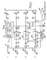
- Referring firstly to Figure 1, the apparatus includes a circuit for detecting when a spark has been created by detecting a voltage spike which remains over 200V for less than 20 µS. The details of the circuit for this purpose are disclosed in copending EP-A-20 069 of even date. As shown in Figure 1, however, this circuit includes a
detector 10 which produces a positive going output signal for as long as its input is at more than 200V. The output ofdetector 10 is applied to one input of a NAND gate 11 the output of which is applied to the input of a monostable circuit 12 which is triggered by a negative going edge at its input and then produces a high output for the following 20 ,uS. The outputs of gate 11 and circuit 12 are applied to two inputs of aNAND gate 13. Thisgate 13 produces a low output only if the output ofdetector 10 goes low again before the output of circuit 12 goes low after 20 µS. The output ofgate 13 is applied via aninverter 14 to a monostable circuit 15 which is negative edge triggered and has oneoutput 15a which goes low for 1 mS following triggering and anotheroutput 15b which goes high for the same period. Theoutput 15a is connected to the other input of gate 11 so as to block this gate for 1 mS following recognition of a spike. - For sensing the re-initiation of current flow in the primary winding there is a
current detector circuit 16 which produces a high output at aterminal 16a whenever the current is in excess of a threshold value.Circuit 16 also has aterminal 16b at which there is a high output in the event of a supply fault as will be hereinafter explained. -
Terminal 16a is connected to one input of a NAND gate 17 the other input of which is connected to the output of a furthermonostable circuit 18 triggered by the same input as circuit 15 and producing a high output for 100 µS after triggering. The output of gate 17 is connected to the input of amonostable circuit 19 which is negative going edge triggered and produces a low output for 4 uS following triggering. The output of the gate 17 is also connected via aninverter 20 to one input of aNAND gate 21, the other input of which is connected via aninverter 22 to the output ofdetector 10. The output ofgate 21 is connected by aresistor 42 and acapacitor 23 in series to earth and the junction of theresistor 42 andcapacitor 23 is connected to the input of aninverter 24. ANAND gate 25 has one input connected to the output ofcircuit 19 and the other to the output ofinverter 24. - The output of
gate 25 is normally high, but goes low if the output atterminal 16a goes low for more than 4 pS whilst the output ofcircuit 18 is high. Themonostable circuit 19 prevents spurious operation of thegate 25 by noise and also delays the output ofgate 25 in the event that the output ofcircuit 16a is already low when the 100 µS pulse fromcircuit 18 commences. This prevents pulse coincidence problems at other points in the circuit. - The output of
gate 25 is connected to one input of aNAND gate 26, the other input of which is connected to the output of aNAND gate 27 which has one input connected toterminal 15b and the other to output ofgate 26. The outputs ofgates NAND gates monostable circuit 30 connected to be triggered by negative-going edges of the output ofcircuit 18 and providing a high output for 200 pS following triggering. - Gates 26 and 27 act as a latch enabled by the 1 mS output of circuit 15 and set (if at all) by the output of
gate 25. As mentioned above theoutput 1 5b of circuit 15 only goes high for 1 mS on recognition of a short duration high voltage spike at the input ofdetector 10. The 100µS circuit 18 is started at the same time as the circuit 15 and if no output is produced bygate 25 during this 100µS period gates gate 26 producing a low output and gate 27 a high output..At the end of the 100 µS period the output ofcircuit 30 goes high so that the output ofgate 29 goes low for 200 µS whilst the output ofgate 28 remains high. In the event ofgate 25 producing a low output during the 100pS period gates gate 26 goes high causing the output ofgate 27 to go low. Whencircuit 30 is triggered the output ofgate 28 goes low for 200 µS, whereas the output ofgate 29 remains high. This is taken to indicate a multiple spark condition. - The output of
gate 29 is connected to the input terminal of a missingpulse detector circuit 31 which is described in detail in copending EP-A-20 071 of even date. During normal steady running operation circuit thegate 29 produces a train of regularly spaced 200 µS negative-going pulses. Thecircuit 31 produces at oneoutput terminal 31 a a negative going 200 pS pulse each time a pulse is missing from the input pulse train. This negative-going pulse is synchronised with the next pulse in the input pulse train. A second output terminal 31 b of thecircuit 31 transmits a positive going 200 pS pulse immediately following each negative going pulse of the input pulse train. - The terminal 31 a is connected to the input terminal of a d.c. triggered
monostable circuit 32 the output of which goes low for 200 µS each time the input thereto goes low. The output ofcircuit 32 is connected by aresistor 33 to the cathode of alight emitting diode 34 which has its anode connected to the +ve supply. Thelight emitting diode 34 is energised each time a missing pulse is detected. - Both outputs 31 a and 31 b of the
missing pulse detector 31 are connected to inputs of a cyclic pulsepattern recognition circuit 35 which is described in detail in copending EP-A-20070 of even date. This circuit includes a cycle length selection switch and produces a negative-going output pulse at anoutput terminal '35a if the same pulse is missed in two successive cycles or a negative going output pulse at asecond output terminal 35b if two pulses are missed within one cycle. These output pulses, if produced are synchronised with the input pulses to circuit 31 (although they may be of shorter duration). - The two
outputs circuit 35 are connected to adisplay control circuit 36 which also has inputs from terminal 31 b, fromgate 28 and fromterminal 16b. Thecircuit 36 controls fourlight emitting diodes - Figure 2 shows the input stages of the test apparatus in more detail in conjunction with an ignition system under test. As shown, the system includes a step-
up coil 50 having a primary winding 50a and asecondary winding 50b. Theprimary winding 50a is connected at one end by aballast resistor 51 to the positive terminal of a battery 52, and at the other end by theoutput transistor 53a of anelectronic switching circuit 53 to earth (i.e. the negative terminal of the battery 52). The secondary winding of thecoil 50 is connected between said one end of the primary winding and a spark circuit 54 having the usual earth return. - The test apparatus which forms the subject of the present invention has
terminals input terminals primary winding 50a. Anadditional terminal 64 is provided for use when the system to be tested does not include a ballast resistor, but uses some other means of limiting the primary current. Theterminal 64 is connected by aresistor 65 to theterminal 60 andterminal 64 is used in these circumstances to supply the primary current to the coil, the normal connection between the primary winding and the battery +ve terminal being broken for this purpose. - The test apparatus includes a first
reference voltage generator 66 which is connected betweenterminals terminal 66a which is a fixed voltage below the voltage on terminal 60). Theterminal 66a is connected by apotentiometer 67 and aresistor 68 in series to theterminal 60 and the variable point of thepotentiometer 67 is connected by two resistors 69 and 70 in series to theterminal 60. - A second
reference voltage generator 71 is connected between theterminal 61 and the cathode of aprotective diode 72 having its anode connected toterminal 60. Thegenerator 71 has twooutput terminals 71a and 71 b at different fixed voltages above the voltage atterminal 61. - A voltage comparator 73 has its non-inverting input connected to the
terminal 71 a and its inverting input connected to the common point of tworesistors diode 72 and earth. The output of comparator 73 is connected by aresistor 76 to the cathode of alight emitting diode 77 the anode of which is connected to a positive supply rail connected to the output of avoltage regulator circuit 78 having its input connected to the cathode ofdiode 72. Thelight emitting diode 77 is energised whenever the battery voltage is above a predetermined minimum. - A voltage comparator 80 has its non-inverting input connected to the junction of two resistors 81, 82 which are in series between the junction of resistors 69, 70 and earth and its inverting input connected to the junction of two
resistors 83, 84 connected in series between the terminal 64 and earth. The output of comparator 80 is connected by aload resistor 85 to the +ve supply rail. Afurther voltage comparator 86 has its non-inverting input connected to the junction of tworesistors 87 and 88 which are in series betweenterminal 66a and earth, and its inverting input connected to the junction of tworesistors comparator 86 is connected by aload resistor 91 to the +ve rail. Aselector switch 92 is connected to select which of the twocomparators 80, 86 has its output connected to theoutput terminal 16a of thecurrent detector 16 of which thecomparators 80, 86 and the associatedreference voltage generator 66 form part. The output of the selectedcomparator 80 or 86 goes high only when there is sufficient current flowing in theballast resistor 51 orsubstitute resistor 65 to take the potential at the inverter input of that comparator below the voltage at the non-inverting input thereto. - A
voltage comparator 93 also forms part of thecircuit 16 and its output is connected to terminal 16b and also by aresistor 94 to the +ve and by acapacitor 95 to earth. The non-inverting input ofcomparator 93 is connected directly to terminal 71b and its inverting input is connected to the junction of tworesistors comparator 93 is high only if the combined voltage drop across thetransistor 53a and the primary winding 50a falls below a threshold level determined by the voltage at terminal 71 b and the ratio of theresistors capacitor 95 ensures that the output ofcomparator 93 does not go high immediately this condition occurs so as to obviate amplification of noise by thecomparator 93. - The 200
V detector circuit 10 includes a voltage comparator 9 having its inverting input connected to the terminal 71 b and its non-inverting input connected to the junction of tworesistors 98, 99 in series betweenterminal 63 and earth. The output of comparator 9 is connected by aresistor 100 to the positive rail and its output is the signal fed to gate 11 andinverter 22 in Figure 1. - Turning now to Figure 3, the terminal 16b is connected to one input of a NAND gate 111, the other input of which is connected to the output of an
inverter 112. The output of gate 111 is connected to one input of aNAND gate 113, the other input of which is connected to the output of aNAND gate 114 and the output of which is connected to one input ofgate 114. The other input ofgate 114 is connected to the output of aNAND gate 115 one input of which is connected to terminal 31 b and the other input of which is connected to the output ofinverter 112. The output ofgate 113 is also connected to one input of aNAND gate 116 the other input of which is connected to the output of aNAND gate 117 to which the input ofinverter 112 is also connected. The output ofgate 116 is connected by aresistor 118 to the cathode oflight emitting diode 37. ANAND gate 119 has one input connected to the output ofgate 114 and its other input connected to the output ofgate 115. - The
output terminal 28a of gate 28 (see Figure 1) is connected via aninverter 120 to one input of aNAND gate 121 the other input of which is connected to the output ofinverter 112. The output ofgate 121 is connected via aninverter 122 to the SET input of a D-type flip-flop circuit 123 having its CLOCK and D inputs grounded and its RESET input connected to the output ofgate 119. The Q output ofcircuit 123 is connected to one input of aNAND gate 124, the other input of which is connected to the output ofgate 117 and the output of which is connected by a resistor 125 to the cathode oflight emitting diode 38. - The terminal 35a of the cyclic
pattern recognition circuit 35 is connected via aninverter 126 to one input of aNAND gate 127 the other input of which is connected to the output ofinverter 112. The output ofgate 127 is connected via aninverter 128 to the SET input of a D-type flip-flop circuit 129 having its CLOCK and D inputs grounded and its RESET input connected to the output of aninverter 130. The Q output ofcircuit 129 is connected by aresistor 131 to the cathode oflight emitting diode 39. - The terminal 35b is connected via an
inverter 132 to one input of aNAND gate 133 the other input of which is connected to the output of theinverter 112 and the output of which is connected via aninverter 134 to the SET input of a D-type flip-flop circuit 135 having its CLOCK and D inputs grounded and its RESET input connected to the output ofinverter 130. The Q output ofcircuit 135 is connected by aresistor 136 to the cathode of the light emitting diode 40. - The
gate 117 has its two inputs connected to the Q outputs ofcircuits - The
inverter 130 has its input connected to the output of aninverter 137, afeedback resistor 138 being connected between the output ofinverter 130 and the input ofinverter 137 which is connected by tworesistors 139, 140 in series to the output ofgate 117, a capacitor 141 connecting the junction ofresistors 139, 140 to earth. This junction is also connected to a switch 142 by means of which it can be selected whether the apparatus will reset automatically after detecting a fault. In the open position shown the capacitor 141 will charge up slowly following the output ofgate 140 going high, until the output ofinverter 130 goes high thereby providing a resetting pulse tocircuits resistors 139 and 140 is connected to areset switch 143 which in its normal position (as shown) connects this junction to earth so that charging of capacitor 141 is prevented. When actuated,switch 143 connects this junction to the +ve rail, thereby charging capacitor 141 rapidly to provide the reset pulse. - After resetting the Q outputs of
circuits gate 117 is low and that ofinverter 112 high. Thusgates gates - In the event of a cyclically repeated missing pulse occurring, the output at
terminal 35a goes low briefly thereby settingcircuit 129 so that the Q output thereof goes low. As a resultlight emitting diode 39 is lit and the output ofgate 117 goes high. In the auto-reset mode capacitor 141 now starts charging up. The output ofinverter 112 goes low thereby blockinggates - In the event of the first fault after resetting being a multiple misfire, i.e. two missing pulses within one cycle the output of
terminal 35b goes low briefly causing circuit 135 Q output to go low, lighting light emitting diode 40, starting the reset operation and blockinggates - The occurrence of a negative going pulse at terminal 28a indicates (as mentioned above) a multiple firing condition. If such a pulse occurs between resetting of
circuits 35b circuit 123 will be set and its Q output will go high.Gate 124 will, however, be blocked by the low output ofgate 117 andcircuit 123 will be reset by the next pulse at terminal 31 b viagates terminal 35b circuitscircuit 135 goes low before the next pulse arrives at terminal 31 b. As a result the operation of the missingpulse detector 31 is arrestedgates gate 124 is enabled so that light emittingdiode 38 is lit.Gate 115 is also blocked so that the following pulses at terminal 316 do not resetcircuit 123 untilcircuit 135 has been reset. - The above paragraph is true only if the signal at
terminal 16b is not high at the same time as the signal at terminal 28a is low. If this condition does occur the output of gate 111 goes low causing the output ofgate 113 to go high thereby causing the output ofgate 114 to go low thereby latchinggates gate 115 goes high, and resettingcircuit 123. The output ofinverter 112 goes low before the next pulse at terminal 31 b thereby blockinggate 115.Gate 116 is enabled and tight emittingdiode 37 is lit instead ofdiode 38.
Claims (7)
Applications Claiming Priority (2)
| Application Number | Priority Date | Filing Date | Title |
|---|---|---|---|
| GB7918389 | 1979-05-25 | ||
| GB7918389 | 1979-05-25 |
Publications (2)
| Publication Number | Publication Date |
|---|---|
| EP0020067A1 EP0020067A1 (en) | 1980-12-10 |
| EP0020067B1 true EP0020067B1 (en) | 1983-11-09 |
Family
ID=10505471
Family Applications (1)
| Application Number | Title | Priority Date | Filing Date |
|---|---|---|---|
| EP80301630A Expired EP0020067B1 (en) | 1979-05-25 | 1980-05-19 | Test apparatus for testing internal combustion engine electronic spark ignition systems |
Country Status (5)
| Country | Link |
|---|---|
| US (1) | US4331921A (en) |
| EP (1) | EP0020067B1 (en) |
| JP (1) | JPS55161974A (en) |
| AU (1) | AU533621B2 (en) |
| DE (1) | DE3065510D1 (en) |
Families Citing this family (9)
| Publication number | Priority date | Publication date | Assignee | Title |
|---|---|---|---|---|
| DE3208587C2 (en) * | 1982-03-10 | 1985-10-31 | Daimler-Benz Ag, 7000 Stuttgart | Device for detecting misfires |
| IT1157997B (en) * | 1982-12-29 | 1987-02-18 | Sic Societa Ind E Di Consulenz | APPARATUS FOR TESTS ON IGNITION DEVICES OF ENDOTHERMAL ENGINES |
| US4689573A (en) * | 1985-08-20 | 1987-08-25 | Switches, Inc. | On-vehicle diagnostic unit for electronic ignition systems |
| EP0384436B1 (en) * | 1989-02-22 | 1994-12-14 | Nippondenso Co., Ltd. | Ignition detecting device of ignition apparatus |
| US5216369A (en) * | 1989-02-22 | 1993-06-01 | Nippondenso Co., Ltd. | Ignition occurrence detecting device for use in an ignition apparatus |
| DE3909906A1 (en) * | 1989-03-25 | 1990-09-27 | Bosch Gmbh Robert | CIRCUIT ARRANGEMENT FOR MONITORING A HIGH VOLTAGE IGNITION SYSTEM |
| FR2768186B1 (en) * | 1997-09-11 | 1999-10-15 | Siemens Automotive Sa | METHOD AND DEVICE FOR DIAGNOSING AN IGNITION SYSTEM FOR AN INTERNAL COMBUSTION ENGINE |
| DE10120142B4 (en) * | 2001-04-25 | 2010-12-30 | Nxp B.V. | Detector circuit for the detection of voltage spikes |
| JP6273988B2 (en) * | 2014-04-10 | 2018-02-07 | 株式会社デンソー | Ignition device for internal combustion engine |
Citations (1)
| Publication number | Priority date | Publication date | Assignee | Title |
|---|---|---|---|---|
| US4101822A (en) * | 1977-03-25 | 1978-07-18 | Owatonna Tool Company | Instrument for testing a breakerless ignition system |
Family Cites Families (5)
| Publication number | Priority date | Publication date | Assignee | Title |
|---|---|---|---|---|
| US3551800A (en) * | 1968-06-06 | 1970-12-29 | Ibm | Test apparatus for analyzing the performance characteristics of internal combustion engine ignition systems |
| DE2040913C3 (en) * | 1970-08-18 | 1978-06-15 | Volkswagenwerk Ag, 3180 Wolfsburg | Device for the automatic detection of the timing of the ignition voltages in a multi-cylinder internal combustion engine |
| SE403508B (en) * | 1974-12-19 | 1978-08-21 | United Technologies Corp | APPLIANCE FOR TESTING THE IGNITION COIL / CONDENSER IN THE IGNITION SYSTEM IGNITION SYSTEM |
| FR2317520A1 (en) * | 1975-07-11 | 1977-02-04 | Renault | END OF IGNITION VOLTAGE ANALYZER OF AN INTERNAL COMBUSTION ENGINE |
| US4112351A (en) * | 1977-09-01 | 1978-09-05 | United Technologies Corporation | Dual threshold low coil signal conditioner |
-
1980
- 1980-05-19 EP EP80301630A patent/EP0020067B1/en not_active Expired
- 1980-05-19 DE DE8080301630T patent/DE3065510D1/en not_active Expired
- 1980-05-21 US US06/151,929 patent/US4331921A/en not_active Expired - Lifetime
- 1980-05-23 AU AU58695/80A patent/AU533621B2/en not_active Ceased
- 1980-05-26 JP JP6906080A patent/JPS55161974A/en active Pending
Patent Citations (1)
| Publication number | Priority date | Publication date | Assignee | Title |
|---|---|---|---|---|
| US4101822A (en) * | 1977-03-25 | 1978-07-18 | Owatonna Tool Company | Instrument for testing a breakerless ignition system |
Also Published As
| Publication number | Publication date |
|---|---|
| DE3065510D1 (en) | 1983-12-15 |
| US4331921A (en) | 1982-05-25 |
| EP0020067A1 (en) | 1980-12-10 |
| AU5869580A (en) | 1980-11-27 |
| AU533621B2 (en) | 1983-12-01 |
| JPS55161974A (en) | 1980-12-16 |
Similar Documents
| Publication | Publication Date | Title |
|---|---|---|
| US4333054A (en) | Apparatus for use in testing an internal combustion engine ignition system | |
| US4886029A (en) | Ignition misfire detector | |
| US4987771A (en) | Misfire detection device for an internal combustion engine | |
| US4112351A (en) | Dual threshold low coil signal conditioner | |
| KR900001444B1 (en) | Engine control apparatus | |
| JPH04232340A (en) | Motion monitor device for ignition system and monitor method, and sound condition diagnosis method and ignition system for ignition plug | |
| US6275041B1 (en) | Combustion state detecting apparatus for internal combustion engine | |
| EP0020067B1 (en) | Test apparatus for testing internal combustion engine electronic spark ignition systems | |
| US4893564A (en) | Electric detonator of delay type | |
| JPH05106545A (en) | Misfiring detection device for gasoline engine | |
| US4008430A (en) | Automotive test apparatus for coupling to the ignition system of automotive internal combustion engines | |
| US4030095A (en) | Pulsed alarm system | |
| US2976485A (en) | Continuity testing device for explosive igniting circuits | |
| US4377835A (en) | Recovery protection device for a thyristor valve | |
| US4331922A (en) | Test apparatus for testing internal combustion spark ignition systems | |
| EP0659999A1 (en) | Diagnostic apparatus and methods for ignition circuits | |
| US4186711A (en) | Ignition device with speed limitation for internal combustion engines | |
| US20050066948A1 (en) | Capacitor discharge ignition device | |
| EP0384436B1 (en) | Ignition detecting device of ignition apparatus | |
| US4502447A (en) | Method of and device for supervising electrical fuel injection systems | |
| US3281810A (en) | Pulse monitoring circuit | |
| US4277752A (en) | Device for testing ignition system of a combustion engine | |
| US4170131A (en) | Single sensor engine analyzer with noise rejection and automatic triggering circuit | |
| JP2665794B2 (en) | Ignition device for internal combustion engine | |
| JPS6019962A (en) | Ignition device for internal-combustion engine |
Legal Events
| Date | Code | Title | Description |
|---|---|---|---|
| PUAI | Public reference made under article 153(3) epc to a published international application that has entered the european phase |
Free format text: ORIGINAL CODE: 0009012 |
|
| AK | Designated contracting states |
Designated state(s): BE DE FR GB IT NL |
|
| 17P | Request for examination filed |
Effective date: 19810224 |
|
| RAP1 | Party data changed (applicant data changed or rights of an application transferred) |
Owner name: LUCAS INDUSTRIES PLC |
|
| ITF | It: translation for a ep patent filed |
Owner name: SOCIETA' ITALIANA BREVETTI S.P.A. |
|
| GRAA | (expected) grant |
Free format text: ORIGINAL CODE: 0009210 |
|
| AK | Designated contracting states |
Designated state(s): BE DE FR GB IT NL |
|
| REF | Corresponds to: |
Ref document number: 3065510 Country of ref document: DE Date of ref document: 19831215 |
|
| ET | Fr: translation filed | ||
| PGFP | Annual fee paid to national office [announced via postgrant information from national office to epo] |
Ref country code: FR Payment date: 19840227 Year of fee payment: 5 |
|
| PGFP | Annual fee paid to national office [announced via postgrant information from national office to epo] |
Ref country code: DE Payment date: 19840526 Year of fee payment: 5 |
|
| PGFP | Annual fee paid to national office [announced via postgrant information from national office to epo] |
Ref country code: BE Payment date: 19840630 Year of fee payment: 5 |
|
| PLBE | No opposition filed within time limit |
Free format text: ORIGINAL CODE: 0009261 |
|
| STAA | Information on the status of an ep patent application or granted ep patent |
Free format text: STATUS: NO OPPOSITION FILED WITHIN TIME LIMIT |
|
| 26N | No opposition filed | ||
| PGFP | Annual fee paid to national office [announced via postgrant information from national office to epo] |
Ref country code: NL Payment date: 19870531 Year of fee payment: 8 |
|
| PG25 | Lapsed in a contracting state [announced via postgrant information from national office to epo] |
Ref country code: GB Effective date: 19880519 |
|
| BERE | Be: lapsed |
Owner name: LUCAS INDUSTRIES P.L.C. Effective date: 19880531 |
|
| PG25 | Lapsed in a contracting state [announced via postgrant information from national office to epo] |
Ref country code: NL Effective date: 19881201 |
|
| NLV4 | Nl: lapsed or anulled due to non-payment of the annual fee | ||
| PG25 | Lapsed in a contracting state [announced via postgrant information from national office to epo] |
Ref country code: FR Free format text: LAPSE BECAUSE OF NON-PAYMENT OF DUE FEES Effective date: 19890131 |
|
| GBPC | Gb: european patent ceased through non-payment of renewal fee | ||
| PG25 | Lapsed in a contracting state [announced via postgrant information from national office to epo] |
Ref country code: DE Effective date: 19890201 |
|
| REG | Reference to a national code |
Ref country code: FR Ref legal event code: ST |
|
| PG25 | Lapsed in a contracting state [announced via postgrant information from national office to epo] |
Ref country code: BE Effective date: 19890531 |