EP0019735A1 - Method and circuit for contrast correction of colour television signals - Google Patents
Method and circuit for contrast correction of colour television signals Download PDFInfo
- Publication number
- EP0019735A1 EP0019735A1 EP80102335A EP80102335A EP0019735A1 EP 0019735 A1 EP0019735 A1 EP 0019735A1 EP 80102335 A EP80102335 A EP 80102335A EP 80102335 A EP80102335 A EP 80102335A EP 0019735 A1 EP0019735 A1 EP 0019735A1
- Authority
- EP
- European Patent Office
- Prior art keywords
- signal
- output
- input
- color
- stage
- Prior art date
- Legal status (The legal status is an assumption and is not a legal conclusion. Google has not performed a legal analysis and makes no representation as to the accuracy of the status listed.)
- Granted
Links
Images

Classifications
-
- H—ELECTRICITY
- H04—ELECTRIC COMMUNICATION TECHNIQUE
- H04N—PICTORIAL COMMUNICATION, e.g. TELEVISION
- H04N9/00—Details of colour television systems
- H04N9/64—Circuits for processing colour signals
- H04N9/68—Circuits for processing colour signals for controlling the amplitude of colour signals, e.g. automatic chroma control circuits
- H04N9/69—Circuits for processing colour signals for controlling the amplitude of colour signals, e.g. automatic chroma control circuits for modifying the colour signals by gamma correction
Definitions
- the invention is based on a method according to the preamble of the main claim.
- the electronic image converters, recording tubes and picture display tubes can often not process the range of contrast in the order of several 100: 1 specified by an original image, natural scene, slide, etc.
- the transmission characteristic becomes in addition to the gamma decryption performed, subjected to an additional contrast correction.
- the method according to the invention with the characterizing features of the main claim has the advantage that it is less complex by using only one multiplier. It is also advantageous that the contrast in the darker parts of the image is corrected particularly intensely.
- the color separation signals R, G, R which are generated by an image signal source not shown in the figure, are fed to a coder 1, which generates a composite uncorrected color signal in accordance with a predefined television standard, for example PAL or NTSC.
- This color signal is fed to the first input of an adder 2.
- the color separation signals also become a non-additive mixing circuit 3, at the output of which a signal corresponding to the greatest brightness can be removed.
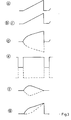
- the signals supplied to circuits 1, 2 and 3 are denoted by a and b in FIG. 3 and the signal which can be taken off at the output of circuit 3 is denoted by c. For example, sawtooth-shaped signals are used.
- the output signal of the circuit 3 is now fed to a signal processing circuit 4 which contains a low-pass element 6 and a non-linear amplifier circuit 7 and 8 each.
- the low-pass element 6 only allows signals of the lower frequency range to pass through, since measures influencing the contrast are expedient only in low-frequency image details.
- the term of the low-pass element 6 is adapted to that of the encoder 1, so that a separate term adjustment can be dispensed with.
- the band-limited signal is fed to a non-linear amplifier stage 7, in which a so-called.
- the signal is "stretched black". A signal according to d (FIG. 3) can then be removed at the output of this stage 7.
- the blanking signal A is fed to the nonlinear amplifier stage 8, which is constructed in the same way as stage 7.
- a control voltage U S t is also supplied at both stages 7 and 8.
- e Fi G. 3
- the signals d and e are now fed to the control inputs of a multiplier 9, at whose further input the signal emitted by the coder 1 is located.
- the contrast correction signal which can be taken off at the output of the multiplier stage 9 must be closed in the blanking interval as well as in the 100% white point Become zero. This can be achieved by forming the difference between the signals d and e, which takes place in the multiplier 9.
- the signal f is then fed to the second input of the adder stage 2 and added to the uncorrected signal, so that a contrast-corrected signal g can be removed at the output of the stage 2.
- FIG. 2 shows a contrast correction circuit for color television signals according to the SECAM standard, the luminance signal Y generated by a matrix not shown in the figure and the line-sequential color difference signal D B / D ⁇ being present at the input terminals 11 and 12.
- These signals with the form b are now fed to the first inputs of an adder 13 and 14, respectively.
- a signal processing circuit 4 is provided, as in FIG. 1, at whose inputs the signal X of the non-additive mixing circuit 3, clamping pulses KI, the blanking signal A and the control voltage U St are present.
- the signals d and e are also removable, which are each fed to a multiplier 16 and 17.
- the other input of the multiplier stage 16 is supplied with the luminance signal and the other input of the multiplier stage 17 with the line-sequential color difference signal D B / D R.
- signals according to f of FIG. 3 can be removed. These signals f are now each fed to the second input of the adder stages 13 and 14.
- the output signal of stage 14 is further fed to a frequency modulator 18, at the output of which the frequency-modulated color difference signal can then be removed.
- This signal and the output signal of stage 13 are now combined in a further adding stage 19, so that a contrast-corrected color television signal according to the SECAM standard can be removed at the output of stage 19.
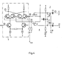
- the output signal X of the circuit 3 and the blanking signal A is present at the terminals 21 and 22 of the stages 7 and 8, respectively. Both signals are fed via a capacitor 23 and 24 to a clamping circuit with a field effect transistor 26 and 27, respectively.
- the field effect transistors 26 and 27 are controlled by the terminal 28 with clamping pulses KI.
- the clamped signal X is now fed to a further field-effect transistor 31, which acts as a voltage-dependent resistor, while the blanking signal, which is also clamped, is fed to a field-effect transistor 32.
- the FET becomes increasingly low-resistance with increasing gate-souice voltage.
- the polarity and the magnitude of this signal voltage can be freely selected with the control voltage U S t.
- the blanking signal A passes through the same circuit as the signal X.
- the signals d and e which are treated in the same way, are fed to the positive and negative control inputs of the multiplier 9, thereby forming a difference between the signals d and e.
- This difference formation ensures that the correction signal f becomes zero in both black and white.
- This circuit also ensures that both the luminance component Y and the chrominance component C of the coded signal are evaluated equally. This does not result in any changes in saturation, which are very disadvantageous in normal black stretching.
Abstract
Description
Die Erfindung geht aus von einem Verfahren nach der Gattung des Hauptanspruchs.The invention is based on a method according to the preamble of the main claim.
Die elektronischen Bildwandler, Aufnahmeröhren und Bildwiedergaberöhren, können wegen ihres eingeschränkten Kontrastumfanges in der Größenordnung 60 : 1 oftmals den von einer Bildvorlage, natürlichen Szene, Diapositiv etc. vorgegebenen Kontrastumfang in der Größenordnung von mehreren 100 : 1 nicht verarbeiten, In diesem Falle wird die Übertragungskennlinie neben der vorgenommenen Gamma-Entzecrung einer zusätzlichen Kontrastkorrektur unterzogen.Due to their limited range of contrast in the order of 60: 1, the electronic image converters, recording tubes and picture display tubes can often not process the range of contrast in the order of several 100: 1 specified by an original image, natural scene, slide, etc. In this case the transmission characteristic becomes in addition to the gamma decryption performed, subjected to an additional contrast correction.
Aus der DE-AS 26 49 781 ist schon eine Vorrichtung zur Kontrastkorrektur für ein Farbfernsehsystem mit mehreren Bildaufnahmeröhren bekannt, welche durch Verwendung von zwei Multiplizierern jedoch relativ aufwendig ist. Außerdem wird hierbei der Kontrast über den gesamten Amplitudenbereich, also bei dunkleren ebenso wie bei helleren Bildteilen, gleichmäßig verändert.From DE-AS 26 49 781 a device for contrast correction for a color television system with several image recording tubes is already known, but this is relatively complex due to the use of two multipliers. In addition, the contrast over the entire amplitude range, i.e. dark as with lighter parts of the picture, evenly changed.
Das erfindungsgemäße Verfahren mit den kennzeichnenden Merkmalen des Hauptanspruchs hat demgegenüber den Vorteil, daß es durch Verwendung nur einer Multiplizierstufe weniger aufwendig ist. Außerdem ist es vorteilhaft, daß der Kontrast in den dunkleren Bildteilen besonders verstärkt korrigiert wird.The method according to the invention with the characterizing features of the main claim has the advantage that it is less complex by using only one multiplier. It is also advantageous that the contrast in the darker parts of the image is corrected particularly intensely.
Durch die in den Unteransprüchen aufgeführten Maßnahmen sind vorteilhafte Weiterbildungen und Verbesserungen des im Hauptanspruch angegebenen Verfahrens möglich.Advantageous further developments and improvements of the method specified in the main claim are possible through the measures listed in the subclaims.
Ausführungsbeispiele der Erfindung sind in der Zeichnung dargestellt und in der nachfolgenden Beschreibung näher erläutert.Embodiments of the invention are shown in the drawing and explained in more detail in the following description.
- Es zeigen: Fig. 1 ein Blockschaltbild der erfindungsgemäßen Schaltung für das PAL- bzw. NTSC-System.,1 shows a block diagram of the circuit according to the invention for the PAL or NTSC system.
- Fig. 2 ein Blockschaltbild der erfindungsgemäßen Schaltung für das SECAM-System,2 is a block diagram of the circuit according to the invention for the SECAM system,
- Fig. 3 einige der in den Figuren 1 und 2 vorkommende Signale,3 shows some of the signals occurring in FIGS. 1 and 2,
- Fig. 4 ein Teilschaltbild zur Erzeugung den Korrektursignals im Detail.Fig. 4 is a partial circuit diagram for generating the correction signal in detail.
In Fig. 1 werden die Farbauszugssignale R, G, R, welche von einer in der Fig. nicht dargestellten Blldsignalquelle erzeugt werden, einem Coder1 zugeführt, welcher entsprechend einer vorgegebenen Fernsehnorm, beispielsweise PAL oder NTSC, ein zusammengesetztes unkorrigiertes Farbsignal erzeugt. Dieses Farbsignal wird dem ersten Eingang einer Addierstufe 2 zugeführt. Die Farbauszugssignale werden außerdem einer Nicht-Additiven-Mischschaltung3zugele, an deren Ausgang ein jeweils der größten Helligkeit entsprechendes Signal abnehmbar ist. Die den Schaltungen 1, 2 und 3 zugeführten Signale sind in Fig. 3 mit a und b und das am Ausgang der Schaltung 3 abnehmbare Signal mit c bezeichnet. Es sind hierbei beispielsweise sägezahnförmige Signale verwendet. Das Ausgangssignal der Schaltung 3 wird nun einer Signalverarbeitungsschaltung 4 zugeführt, welche ein Tiefpaßglied 6 und je eine nichtlineare Verstärkerschaltung 7 und 8 enthält. Das Tiefpaßglied 6 läßt nur Signale des unteren Frequenzbereiches durch, da kontrastbeeinflussende Maßnahmen lediglich in tieffrequenten Bilddetails zweckmäßig sind. Die Laufzeit des Tiefpaßgliedes 6 ist der des Coders 1 angepaßt, so daß auf eine separate Laufzeitanpassung verzichtet werden kann. Danach wird das bandbegrenzte Signal einer nichtlinearen Verstärkerstufe 7 zugeführt, in welcher eine sogen. "Schwarzdehnung" des Signals erfolgt. Am Ausgang dieser Stufe 7 ist dann ein Signal gemäß d (Fig. 3) abnehmbar. Der nichtlinearen Verstärkerstufe 8, welche ebenso aufgebaut ist wie die Stufe 7, wird das Austastsignal A zugeführt. An beiden Stufen 7 und 8 werden neben Klemmimpulsen auch eine Steuerspannung USt zugeführt. Am Ausgang der Stufe 8 ist dann ein Signal gemäß e (FiG. 3) abnehmbar. Die Signale d und e werden nun den Steuereingängen einer Multiplizierstufe 9 zugeleitet, an deren weiterem Eingang das vom Coder 1 abgegebene Signal liegt. Das am Ausgang der Multiplizierstufe 9 abnehmbare Kontrastkorrektursignal muß in der Austastlücke als auch im 100%-Weißpunkt zu Null werden. Dies kann erreicht werden durch Differenzbildung der Signale d und e, welche in der Multiplizierstufe 9 erfolgt. Das Signal f wird dann dem zweiten Eingang der Addierstufe 2 zugeführt und dem nichtkorrigierten Signal zugesetzt, so daß am Ausgang der Stufe 2 ein kontrastkorrigiertes Signal g abnehmbar ist.In FIG. 1, the color separation signals R, G, R, which are generated by an image signal source not shown in the figure, are fed to a
In Fig. 2 ist eine Kontrastkorrektur-Schaltung für Farbfernsehsignale nach der SECAM-Norm dargestellt, wobei an den Eingangsklemmen 11 und 12 das von einer in der Fig. nicht dargestellten Matrix erzeugte Luminanzsignal Y und das zeilensequentielle Farbdifferenzsignal DB/Dß anliegen. Diese Signale mit der Form b werden nun den ersten Eingängen je einer Addierstufe 13 und 14 zugeführt. Hierbei ist ebenfalls eine Signalverarbeitungsschaltung 4 wie in Fig. 1 vorgesehen, an deren Eingängen das Signal X der Nicht-Additiven-Mischschaltung 3, Klemmimpulse KI, das Austastsignal A sowie die Steuerspannung USt anliegen. An deren Ausgang sind ebenfalls die Signale d und e abnehmbar, welche je einer Multiplizierstufe 16 und 17 zugeführt werden. Dem anderen Eingang der Multiplizierstufe 16 wird das Luminanzsignal und dem anderen Eingang der Multiplizierstufe 17 das zeilensequentielle Farbdifferenzsignal DB/DR zugeführt. An den Ausgängen der Stufen 16 und 17 sind Signale gemäß f der Fig. 3 abnehmbar. Diese Signale f werden nun jeweils den zweiten Eingang der Addierstufe 13 und 14 zugeführt. Das Ausgangssignal der Stufe 14,wird weiterhin einem Frequenzmodulator 18 zugeleitet, an dessen Ausgang dann das frequenzmodulierte Farbdifferenzsignal abnehmbar ist. Dieses Signal sowie das Ausgangssignal der Stufe 13 werden nun in einer weiteren Addierstufe 19 zusammengesetzt, so daß am Ausgang der Stufe 19 ein kontrastkorrigiertes Farbfernsehsignal gemäß der SECAM-Norm abnehmbar ist.2 shows a contrast correction circuit for color television signals according to the SECAM standard, the luminance signal Y generated by a matrix not shown in the figure and the line-sequential color difference signal D B / D β being present at the
In Fig. 4 sind die nichtlinearen Verstärker 7 und 8 sowie die Multiplizierstufe 9 im Detail dargestellt. An den Klemmen 21 bzw. 22 der Stufen 7 bzw. 8 liegt das Ausgangssignal X der Schaltung 3 bzw. das Austastsignal A. Beide Signale werden über je einen Kondensator 23 bzw. 24 je einer Klemmschaltung mit einem Feldeffekttransistor 26 bzw.27 zugeführt. Die Feldeffekttransistoren 26 und 27 werden mit Klemmimpulsen KI von der Klemme 28 gesteuert. Das geklemmte Signal X wird nun einem als spannungsabhängigen Widerstand wirkenden weiteren Feldeffekttransistor 31 zugeführt, während das ebenfalls geklemmte Austastsignal einem Feldeffekttransistor 32 zugeführt wird. Liegt beispielsweise an der Gate-Elektrode des FET 31 eine sägezahnförmige Spannung, so wird der FET mit steigender Gate-Souice-Spannung immer niederohmiger. Dadurch entsteht an der Drain-Elektrode ein Signal gemäß d in Fig. 3. Die Polarität und die Größe dieser Signalspannung ist mit der Steuerspannung USt frei wählbar. Das Austastsignal A durchläuft eine ebensolche Schaltung wie das Signal X. Die dadurch gleichbehandelten Signale d und e werden dem positiven sowie negativen Steuereingang der Multiplizierstufe 9 zugeführt, wodurch eine Differenz zwischen den Signalen d und e gebildet wird. Durch diese Differenzbildung wird erreicht, daß das Korrektursignal f im Schwarzen wie im Weißen zu Null wird. Durch diese Schaltung ist auch sichergestellt, daß sowohl der Luminanzanteil Y als auch der Chrominanzanteil C des codierten Signals gleichermaßen bewertet wird. Dadurch ergeben sich keinerlei Sättigungsänderungen, die bei normaler Schwarzdehnung sehr nachteilig in Erscheinung treten.4 shows the
Claims (6)
Priority Applications (1)
| Application Number | Priority Date | Filing Date | Title |
|---|---|---|---|
| AT80102335T ATE3352T1 (en) | 1979-05-25 | 1980-04-30 | METHOD AND CIRCUIT FOR CONTRAST CORRECTION OF COLOR TELEVISION SIGNALS. |
Applications Claiming Priority (2)
| Application Number | Priority Date | Filing Date | Title |
|---|---|---|---|
| DE2921246 | 1979-05-25 | ||
| DE19792921246 DE2921246A1 (en) | 1979-05-25 | 1979-05-25 | METHOD AND CIRCUIT FOR CONTRAST CORRECTION OF COLOR TELEVISION SIGNALS |
Publications (2)
| Publication Number | Publication Date |
|---|---|
| EP0019735A1 true EP0019735A1 (en) | 1980-12-10 |
| EP0019735B1 EP0019735B1 (en) | 1983-05-11 |
Family
ID=6071699
Family Applications (1)
| Application Number | Title | Priority Date | Filing Date |
|---|---|---|---|
| EP80102335A Expired EP0019735B1 (en) | 1979-05-25 | 1980-04-30 | Method and circuit for contrast correction of colour television signals |
Country Status (5)
| Country | Link |
|---|---|
| US (1) | US4305090A (en) |
| EP (1) | EP0019735B1 (en) |
| JP (1) | JPS55158789A (en) |
| AT (1) | ATE3352T1 (en) |
| DE (2) | DE2921246A1 (en) |
Families Citing this family (5)
| Publication number | Priority date | Publication date | Assignee | Title |
|---|---|---|---|---|
| FR2503970B1 (en) * | 1981-04-14 | 1985-10-18 | Lgt Lab Gen Telecomm | SELECTIVE EFFICIENCY NON-LINEARITY CORRECTION DEVICE AND TELEVISION EQUIPMENT COMPRISING SUCH A DEVICE |
| JP2952488B2 (en) * | 1988-11-04 | 1999-09-27 | 富士写真フイルム 株式会社 | Image quality correction method for imaging device |
| US5068718A (en) * | 1988-11-04 | 1991-11-26 | Fuji Photo Film Co., Ltd. | Image quality correcting system for use with an imaging apparatus |
| US5363318A (en) * | 1992-03-23 | 1994-11-08 | Eastman Kodak Company | Method and apparatus for adaptive color characterization and calibration |
| US5394195A (en) * | 1993-06-14 | 1995-02-28 | Philips Electronics North America Corporation | Method and apparatus for performing dynamic gamma contrast control |
Citations (2)
| Publication number | Priority date | Publication date | Assignee | Title |
|---|---|---|---|---|
| US3684825A (en) * | 1971-02-19 | 1972-08-15 | Rca Corp | Contrast compression circuits |
| DE2348588A1 (en) * | 1973-09-27 | 1975-04-24 | Bosch Fernsehanlagen | Gamma correction of colour television transmission systems - involves applying uncorrected signals to two inputs of fading circuit |
Family Cites Families (4)
| Publication number | Priority date | Publication date | Assignee | Title |
|---|---|---|---|---|
| JPS5145451B2 (en) * | 1971-10-27 | 1976-12-03 | ||
| JPS494443A (en) * | 1972-04-25 | 1974-01-16 | ||
| US4167750A (en) * | 1975-02-20 | 1979-09-11 | Matsushita Electric Industrial Co., Ltd. | Color-difference signal modifying apparatus |
| GB1524720A (en) * | 1976-09-16 | 1978-09-13 | Marconi Co Ltd | Contrast correction arrangements |
-
1979
- 1979-05-25 DE DE19792921246 patent/DE2921246A1/en not_active Withdrawn
-
1980
- 1980-04-30 AT AT80102335T patent/ATE3352T1/en not_active IP Right Cessation
- 1980-04-30 DE DE8080102335T patent/DE3063060D1/en not_active Expired
- 1980-04-30 EP EP80102335A patent/EP0019735B1/en not_active Expired
- 1980-05-15 US US06/149,946 patent/US4305090A/en not_active Expired - Lifetime
- 1980-05-26 JP JP6907880A patent/JPS55158789A/en active Granted
Patent Citations (2)
| Publication number | Priority date | Publication date | Assignee | Title |
|---|---|---|---|---|
| US3684825A (en) * | 1971-02-19 | 1972-08-15 | Rca Corp | Contrast compression circuits |
| DE2348588A1 (en) * | 1973-09-27 | 1975-04-24 | Bosch Fernsehanlagen | Gamma correction of colour television transmission systems - involves applying uncorrected signals to two inputs of fading circuit |
Also Published As
| Publication number | Publication date |
|---|---|
| DE2921246A1 (en) | 1980-12-04 |
| JPS55158789A (en) | 1980-12-10 |
| US4305090A (en) | 1981-12-08 |
| EP0019735B1 (en) | 1983-05-11 |
| JPH0316838B2 (en) | 1991-03-06 |
| DE3063060D1 (en) | 1983-06-16 |
| ATE3352T1 (en) | 1983-05-15 |
Similar Documents
| Publication | Publication Date | Title |
|---|---|---|
| AT390860B (en) | CHROMINANCE SIGNAL PROCESSING CIRCUIT | |
| DE2207536A1 (en) | Contrast compression circuit for a color television system | |
| DE2325499A1 (en) | APERTURE CORRECTION CIRCUIT FOR A TELEVISION SIGNAL | |
| DE3143653C2 (en) | ||
| DE3223605C2 (en) | Method and apparatus for preventing false color signals from occurring in color television cameras | |
| DE2018149C3 (en) | Process for increasing the sharpness of color television pictures and circuit arrangement for carrying out the process | |
| DE3620990C2 (en) | Method and circuit arrangement for the non-linear transmission of a video signal | |
| DE2850856C2 (en) | TV camera circuit with a gamma and an aperture correction circuit | |
| DE3238696A1 (en) | COLOR KEY SIGNAL GENERATOR | |
| EP0554938B1 (en) | Method for contrast correction | |
| DE2937958C2 (en) | Process for horizontal and vertical contour correction | |
| DE3412529A1 (en) | NOISE REDUCTION CIRCUIT FOR A VIDEO SIGNAL | |
| EP0019735B1 (en) | Method and circuit for contrast correction of colour television signals | |
| DE2905264A1 (en) | CIRCUIT TO A COLOR IMAGE RECORDING DEVICE | |
| DE2237784A1 (en) | CIRCUIT ARRANGEMENT FOR CHANGING THE COLOR TYPE | |
| DE2144745C3 (en) | System for correcting color television signals | |
| DE3141257A1 (en) | COLOR SIGNAL PROCESSING CIRCUIT | |
| EP0185195B1 (en) | White-compression circuit for video signals | |
| DE3027054A1 (en) | METHOD FOR DERIVING A DIGITAL CONTROL SIGNAL | |
| DE2711586C3 (en) | Circuit for generating special effects on color television pictures, in particular for titling | |
| DE4017878A1 (en) | Deriving key signal from foreground of video signal - using three=dimensional zone enclosed on all sides for increased colour possibilities | |
| DE3619663A1 (en) | SYSTEM FOR CORRECTING A LUMINANCE SIGNAL | |
| DE2649781B2 (en) | Contrast correction device for a color television system having a plurality of image pickup tubes | |
| DE3633716A1 (en) | Method and circuit for reducing interference due to cross-colour | |
| DE2013219C3 (en) | Circuit arrangement for correcting the video signals supplied by a television camera with a gamma correction circuit |
Legal Events
| Date | Code | Title | Description |
|---|---|---|---|
| PUAI | Public reference made under article 153(3) epc to a published international application that has entered the european phase |
Free format text: ORIGINAL CODE: 0009012 |
|
| AK | Designated contracting states |
Designated state(s): AT BE CH DE FR GB IT NL |
|
| 17P | Request for examination filed |
Effective date: 19801117 |
|
| GRAA | (expected) grant |
Free format text: ORIGINAL CODE: 0009210 |
|
| AK | Designated contracting states |
Designated state(s): AT BE CH DE FR GB IT LI NL |
|
| PG25 | Lapsed in a contracting state [announced via postgrant information from national office to epo] |
Ref country code: IT Free format text: LAPSE BECAUSE OF FAILURE TO SUBMIT A TRANSLATION OF THE DESCRIPTION OR TO PAY THE FEE WITHIN THE PRESCRIBED TIME-LIMIT;WARNING: LAPSES OF ITALIAN PATENTS WITH EFFECTIVE DATE BEFORE 2007 MAY HAVE OCCURRED AT ANY TIME BEFORE 2007. THE CORRECT EFFECTIVE DATE MAY BE DIFFERENT FROM THE ONE RECORDED. Effective date: 19830511 |
|
| REF | Corresponds to: |
Ref document number: 3352 Country of ref document: AT Date of ref document: 19830515 Kind code of ref document: T |
|
| REF | Corresponds to: |
Ref document number: 3063060 Country of ref document: DE Date of ref document: 19830616 |
|
| ET | Fr: translation filed | ||
| PLBE | No opposition filed within time limit |
Free format text: ORIGINAL CODE: 0009261 |
|
| STAA | Information on the status of an ep patent application or granted ep patent |
Free format text: STATUS: NO OPPOSITION FILED WITHIN TIME LIMIT |
|
| 26N | No opposition filed | ||
| PGFP | Annual fee paid to national office [announced via postgrant information from national office to epo] |
Ref country code: CH Payment date: 19840730 Year of fee payment: 5 |
|
| PG25 | Lapsed in a contracting state [announced via postgrant information from national office to epo] |
Ref country code: LI Effective date: 19860430 Ref country code: CH Effective date: 19860430 |
|
| REG | Reference to a national code |
Ref country code: CH Ref legal event code: PL |
|
| PGFP | Annual fee paid to national office [announced via postgrant information from national office to epo] |
Ref country code: NL Payment date: 19870430 Year of fee payment: 8 |
|
| PGFP | Annual fee paid to national office [announced via postgrant information from national office to epo] |
Ref country code: AT Payment date: 19890424 Year of fee payment: 10 |
|
| PG25 | Lapsed in a contracting state [announced via postgrant information from national office to epo] |
Ref country code: NL Effective date: 19891101 |
|
| NLV4 | Nl: lapsed or anulled due to non-payment of the annual fee | ||
| REG | Reference to a national code |
Ref country code: GB Ref legal event code: 746 |
|
| PG25 | Lapsed in a contracting state [announced via postgrant information from national office to epo] |
Ref country code: AT Effective date: 19900430 |
|
| PGFP | Annual fee paid to national office [announced via postgrant information from national office to epo] |
Ref country code: GB Payment date: 19940420 Year of fee payment: 15 |
|
| PGFP | Annual fee paid to national office [announced via postgrant information from national office to epo] |
Ref country code: FR Payment date: 19940429 Year of fee payment: 15 |
|
| PGFP | Annual fee paid to national office [announced via postgrant information from national office to epo] |
Ref country code: DE Payment date: 19940628 Year of fee payment: 15 |
|
| PGFP | Annual fee paid to national office [announced via postgrant information from national office to epo] |
Ref country code: BE Payment date: 19940715 Year of fee payment: 15 |
|
| PG25 | Lapsed in a contracting state [announced via postgrant information from national office to epo] |
Ref country code: GB Effective date: 19950430 Ref country code: BE Effective date: 19950430 |
|
| BERE | Be: lapsed |
Owner name: ROBERT BOSCH G.M.B.H. Effective date: 19950430 |
|
| PG25 | Lapsed in a contracting state [announced via postgrant information from national office to epo] |
Ref country code: FR Effective date: 19951229 |
|
| GBPC | Gb: european patent ceased through non-payment of renewal fee |
Effective date: 19950430 |
|
| PG25 | Lapsed in a contracting state [announced via postgrant information from national office to epo] |
Ref country code: DE Effective date: 19960103 |
|
| REG | Reference to a national code |
Ref country code: FR Ref legal event code: ST |