EP0019269B1 - Method and circuit for separating the thermal background signal of an ir detector from the desired signal - Google Patents
Method and circuit for separating the thermal background signal of an ir detector from the desired signal Download PDFInfo
- Publication number
- EP0019269B1 EP0019269B1 EP80102670A EP80102670A EP0019269B1 EP 0019269 B1 EP0019269 B1 EP 0019269B1 EP 80102670 A EP80102670 A EP 80102670A EP 80102670 A EP80102670 A EP 80102670A EP 0019269 B1 EP0019269 B1 EP 0019269B1
- Authority
- EP
- European Patent Office
- Prior art keywords
- detector
- signal
- capacitors
- infra
- voltage
- Prior art date
- Legal status (The legal status is an assumption and is not a legal conclusion. Google has not performed a legal analysis and makes no representation as to the accuracy of the status listed.)
- Expired
Links
Images

Classifications
-
- F—MECHANICAL ENGINEERING; LIGHTING; HEATING; WEAPONS; BLASTING
- F41—WEAPONS
- F41G—WEAPON SIGHTS; AIMING
- F41G7/00—Direction control systems for self-propelled missiles
- F41G7/20—Direction control systems for self-propelled missiles based on continuous observation of target position
- F41G7/22—Homing guidance systems
- F41G7/224—Deceiving or protecting means
-
- H—ELECTRICITY
- H04—ELECTRIC COMMUNICATION TECHNIQUE
- H04N—PICTORIAL COMMUNICATION, e.g. TELEVISION
- H04N5/00—Details of television systems
- H04N5/30—Transforming light or analogous information into electric information
- H04N5/33—Transforming infrared radiation
Definitions
- the invention relates to a method for separating the thermal background signal of an IR detector from the useful signal with a device for periodically dimming the detector and using two capacitors of the same capacity for storing charges proportional to the useful and background signals and for generating a differential voltage proportional to the useful signal and a circuit arrangement for carrying out the method.
- the recording of images using the IR radiation of the object to be recorded has the disadvantage that the radiation differences of the object to be recorded are often very small, in particular if IR radiation emanates from objects of almost the same temperature.
- the radiation, the intensity of which differs from that of the thermal background signal, essentially forms the useful signal.
- Thermal background radiation also occurs when the IR detector used to record the IR radiation emanating from the object to be photographed is covered by the radiation to be recorded, since it is known that the diaphragm also emits IR radiation.
- the invention is based on a circuit arrangement for recording an object or a landscape by means of the IR radiation emanating from it, in which several IR detectors are used for image recording, which are periodically dimmed to eliminate the thermal background radiation.
- GB-PS 1 229 820 it is proposed to use a single storage capacitor in a bridge circuit in such a way that it serves simultaneously as a memory for the sum signal (from the useful and background signal) and as a memory for the background signal alone.
- the capacitor is charged by the current of the exposed detector for a predeterminable period of time and discharged by the current of the now unexposed detector for a subsequent, equally long period of time. The remaining amount of charge forms the useful signal.
- This system requires a large number of switches and complicated control logic.
- Claim 1 specifies the teaching for signal processing and claims 2 to 4 advantageous embodiments of the invention.
- the resulting voltage difference across the electrodes of a charge transfer element generates charges that are exactly proportional to the useful signal , so that a high linearity of the signal conversion is achieved and conversion errors due to manufacturing tolerances of the components are largely avoided.
- the maximum possible signal amplitude is limited by the respective discharge of the capacitors by the detector current, so that no overloading of the components can occur with large detector irradiation (antiblooming).
- the design of the circuit arrangement according to claim 2 can be integrated in a space-saving manner.
- the IR detectors can advantageously be integrated in the same semiconductor chip and since the spatial size of the circuit arrangement according to the invention is in the same order of magnitude as the IR detector, it can be provided once for each detector. In this way, IR detector arrays can be produced whose output signals can be evaluated with little effort.
- circuit arrangement according to the invention is expediently implemented in MOS planar technology, since charge transfer elements, IR detectors and capacitors can be produced simply and reliably and without substantial specimen scatter.
- Fig. 1, 1 denotes an IR detector element, one end of which is at reference potential (ground) and the other end of which is on the one hand via a first field effect transistor (FET) T1 with a first capacitor C1 and on the other hand via a second FETT2 can be connected to a second capacitor C2.
- the connection point of transistor T1 and capacitor C1 is also connected to a first control electrode G1 of a charge transfer element 4 and can be connected to a reference voltage source U R via a third FETT3.
- the connection point of transistor T2 and capacitor C2 is connected to a second control electrode G2 of the charge transfer element 4 and can be connected to the reference voltage U R via a fourth FETT4.
- the respective other connections of the capacitors C1 and C2 and the reference voltage source U R are at a constant potential, in the exemplary embodiment at ground potential.
- the charge transfer element 4 has a substrate made of P-conducting silicon with a doped N-conducting layer 2, over which the control electrodes G1, G2,... Are applied insulated in a manner known per se.
- the control electrodes G4, G5, ... serve for charge transfer of the charge introduced by means of a PN junction which forms a diode between a P + region 3 connected to a diode voltage UO and the N region 2.
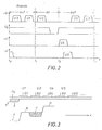
- the IR detector is periodically exposed and the gate electrodes of the FET T1 to T4 are driven in accordance with the pulse schedule shown in FIG. 2.
- P-type MOS FETs are provided, so that they are blocked at a gate voltage of zero volts and are conductive at, for example, 15 volts.
- the ground is at reference potential and the reference voltage source U R has 15 volts.
- the amplitudes of the voltages shown in Fig. 2 also have - 15 volts.
- the transistors T3 and T4 are always driven simultaneously, so that their gates are connected to one another.
- the IR detector is exposed to the useful radiation.
- the gate voltage U3 first opens the transistors T3 and T4. During this time, the gate voltages U1 and U2 of the transistors T1 and T2 are zero and thus the transistors T1 and T2 are blocked.
- the capacitors C1 and C2, which have the same capacitance, are now charged to the reference voltage U R via the transistors T3 and T4.
- the voltage U1 is first applied, which opens the transistor T1, so that the capacitor C1 is now correspondingly across the IR detector 1 irradiated by the useful voltage the intensity of the radiation can discharge to the voltage value U C1 .
- the transistor T1 is blocked and the shutter closed at time t 1 (see FIG. 2), so that when the transistor T2 is opened by the gate voltage U2, the capacitor C2 discharges to the voltage U c2 in accordance with the intensity of the thermal background radiation becomes.
- the voltage U C1 is now at the control electrode G1 and the voltage U c2 at the control electrode G2.
- the diode voltage U o is then controlled to zero volts. This allows a positive charge consisting of holes to flow under the control electrodes G1 and G2. If, at time t 2, the diode voltage U o is brought back to , for example, -15 volts, a local potential curve results, as is shown in FIG. 3.
- x is a location coordinate.
- the voltage U4 is still zero volts at the time t 2 .
- the charge located in area C can therefore not flow off in the direction of area D, but in the direction of area A only as far as the potential threshold in area B allows.
- the charge in area C is now by the control voltages U4, U5 and following, which in a manner known per se to the control electro the G4, G5 and subsequent ones are pushed through the charge transfer element and can be tapped at its output.
Description
Die Erfindung betrifft ein Verfahren zur Trennung des thermischen Hintergrundsignals eines IR-Detektors vom Nutzsignal mit einer Einrichtung zur periodischen Abblendung des Detektors und unter Verwendung zweier Kondensatoren gleicher Kapazität zum Speichern von dem Nutz- und dem Hintergrundsignal proportionalen Ladungen und zur Erzeugung einer dem Nutzsignal proportionalen Differenzspannung und eine Schaltungsanordnung zur Durchführung des Verfahrens.The invention relates to a method for separating the thermal background signal of an IR detector from the useful signal with a device for periodically dimming the detector and using two capacitors of the same capacity for storing charges proportional to the useful and background signals and for generating a differential voltage proportional to the useful signal and a circuit arrangement for carrying out the method.
Die Aufnahme von Bildern unter Verwendung der IR-Strahlung des Aufnahmegegenstandes hat den Nachteil, daß die Strahlungsunterschiede des Aufnahmegegenstandes oft sehr gering sind, insbesondere, wenn IR-Strahlung von Gegenständen nahezu gleicher Temperatur ausgeht. Die Strahlung, deren Intensität sich von der des thermischen Hintergrundsignals unterscheidet, bildet im wesentlichen das Nutzsignal.The recording of images using the IR radiation of the object to be recorded has the disadvantage that the radiation differences of the object to be recorded are often very small, in particular if IR radiation emanates from objects of almost the same temperature. The radiation, the intensity of which differs from that of the thermal background signal, essentially forms the useful signal.
Thermische Hintergrundstrahlung tritt auch dann auf, wenn der zur Aufnahme der vom Aufnahmegegenstand ausgehenden IR-Strahlung verwendete IR-Detektor durch eine Blende von der aufzunehmenden Strahlung abgedeckt wird, da bekanntlich auch die Blende eine IR-Strahlung emittiert.Thermal background radiation also occurs when the IR detector used to record the IR radiation emanating from the object to be photographed is covered by the radiation to be recorded, since it is known that the diaphragm also emits IR radiation.
Die Erfindung geht aus von einer Schaltungsanordnung zur Aufnahme eines Gegenstandes oder einer Landschaft mittels der von ihr ausgehenden IR-Strahlung, bei der zur Bildaufnahme mehrere IR-Detektoren benutzt werden, die zur Eliminierung der thermischen Hintergrundstrahlung periodisch abgeblendet werden.The invention is based on a circuit arrangement for recording an object or a landscape by means of the IR radiation emanating from it, in which several IR detectors are used for image recording, which are periodically dimmed to eliminate the thermal background radiation.
Es ist bekannt, zur Eliminierung der Hintergrundstrahlung jedem IR-Detektor einen eigenen Verstärker zuzuordnen und dessen jeweiligen Verstärkungsgrad an die exemplarstreuungsbedingte unterschiedliche Empfindlichkeit der IR-Detektoren anzupassen, derart, daß die Ausgangssignale der jeweiligen Verstärker bei gleicher IR-Bestrahlung der Detektoren gleiche Ausgangssignale abgeben. Mittels einer weiteren SChwellenschaltung oder eines Differenzverstärkers wird anschließend vom Nutzsignal ein dem Hintergrundsignal entsprechender Betrag subtrahiert, so daß eine Erhöhung des Bildkontrastes erzielt wird.It is known to assign a separate amplifier to each IR detector in order to eliminate the background radiation and to adapt its respective amplification level to the different sensitivity of the IR detectors due to the scattering of the specimen, such that the output signals of the respective amplifiers emit the same output signals with the same IR radiation of the detectors. By means of a further threshold circuit or a differential amplifier, an amount corresponding to the background signal is then subtracted from the useful signal, so that an increase in the image contrast is achieved.
Die bekannten Schaltungsanordnungen haben jedoch den Nachteil, daß für jeden Detektor ein eigener Verstärker erforderlich ist, der außerdem abgeglichen werden muß. Die bekannten Lösungen erfordern folglich viel Platz, Aufwand und Justierarbeit.However, the known circuit arrangements have the disadvantage that a separate amplifier is required for each detector, which amplifier must also be adjusted. The known solutions therefore require a lot of space, effort and adjustment work.
Aus der US-PS 3845 295 ist es bekannt, von einem Bildsignal (frame), welches Nutzsignal und Hintergrundsignal enthält, jeweils das folgende Bildsignal, welches nur Hintergrundsignal enthält, zu subtrahieren, um so zum gewünschten Nutzsignal zu gelangen.From US-PS 3845 295 it is known to subtract the following image signal, which only contains the background signal, from an image signal (frame) which contains the useful signal and the background signal, in order to arrive at the desired useful signal.
In der GB-PS 1 229 820 wird vorgeschlagen, einen einzigen Speicherkondensator in einem Brückenkreis derart zu verwenden, daß er gleichzeitig als Speicher für das Summensignal (aus Nutz- und Hintergrundsignal) wie auch als Speicher für das Hintergrundsignal allein dient. Hierzu wird der Kondensator während einer vorgebbaren Zeitdauer vom Strom des belichteten Detektors aufgeladen und während einer anschließenden, gleich langen Zeitdauer durch den Strom des nun unbelichteten Detektors entladen. Die verbleibende Ladungsmenge bildet das Nutzsignal. Dieses System erfordert eine große Anzahl von Schaltern und eine komplizierte Steuerlogik.In GB-
Bei der US-PS 3 969 634 wird zur besseren Trennung des Nutzsignals vom Hintergrundsignal stets eine konstante Ladungsmenge von der gesamten, einen Bildpunkt zugeordneten Ladungsmenge subtrahiert. Lediglich der Überschuß wird weiterverarbeitet. Hierbei wird offensichtlich eine sehr geringe Streuung der Empfindlichkeit der Infrarot-Detektoren vorausgesetzt. Tatsächlich liegt jedoch die Empfindlichkeitsstreuung und damit die Streuung der erzeugten Ladungsmenge einer Vielzahl von Detektoren bei gleicher Belichtung bei 20 %. Unter Berücksichtigung dieser Streuung ist der erzielbare Gewinn an Störabstand zwischen Nutzsignal und Hintergrundsignal relativ gering, so daß die Auflösung von Bildern unter Verwendung der Infrarot-Strahlung nicht befriedigt.In US Pat. No. 3,969,634, a constant amount of charge is always subtracted from the total amount of charge assigned to a pixel in order to better separate the useful signal from the background signal. Only the surplus is processed. This obviously presupposes a very small spread in the sensitivity of the infrared detectors. In fact, however, the sensitivity spread and thus the spread of the amount of charge generated by a large number of detectors with the same exposure is 20%. Taking this scatter into account, the achievable gain in signal-to-noise ratio between the useful signal and the background signal is relatively small, so that the resolution of images using infrared radiation is unsatisfactory.
Der Erfindung liegt die Aufgabe zugrunde, den bekannten Stand der Technik zu verbessern. Insbesondere soll eine Schaltungsanordnung angegeben werden, welche möglichst wenig Platz beansprucht, nicht abgeglichen zu werden braucht, bei der möglichst viele IR-Detektoren auf einem Halbleiter-Chip inklusive Auswerteeinheiten integrierbar sind und die eine bessere Trennung des Nutzsignals vom Hintergrundsignal ermöglicht.The invention has for its object to improve the known prior art. In particular, a circuit arrangement is to be specified which takes up as little space as possible, does not need to be adjusted, in which as many IR detectors as possible can be integrated on a semiconductor chip, including evaluation units, and which enables the useful signal to be better separated from the background signal.
Die Aufgabe wird durch die im Anspruch 1 angegebene Erfindung gelöst. Dabei geben Anspruch 1 die Lehre für die Signalverarbeitung und die Ansprüche 2 bis 4 vorteilhafte Ausgestaltungen der Erfindung an.The object is achieved by the invention specified in
Dadurch, daß von zwei auf gleiche Spannung geladenen Kondensatoren gleicher Kapazität der eine Kondensator durch den belichteten Detektor, der andere während der gleichen Zeit durch den unbelichteten Detektor entladen wird, erzeugt die entstehende Spannungsdifferenz über die Elektroden eines Ladungstransferelementes Ladungen, die dem Nutzsignal exakt proportional sind, so daß eine hohe Linearität der Signalumwandlung erzielt und Umwandlungsfehler durch Fertigungstoleranzen der Bauelemente weitgehend vermieden werden. Außerdem ist durch die jeweilige Entladung der Kondensatoren durch den Detektorstrom die maximal mögliche Signalamplitude begrenzt, so daß bei großer Detektorbestrahlung keine Übersteuerung der Bauelemente auftreten kann (Antiblooming).Because two capacitors of the same capacity charged to the same voltage discharge one capacitor through the exposed detector and the other through the unexposed detector during the same time, the resulting voltage difference across the electrodes of a charge transfer element generates charges that are exactly proportional to the useful signal , so that a high linearity of the signal conversion is achieved and conversion errors due to manufacturing tolerances of the components are largely avoided. In addition, the maximum possible signal amplitude is limited by the respective discharge of the capacitors by the detector current, so that no overloading of the components can occur with large detector irradiation (antiblooming).
Die Ausgestaltung der Schaltungsanordnung nach Anspruch 2 läßt sich in vorteilhafter Weise raumsparend integrieren. Die IR-Detektoren können in vorteilhafter Weise in das gleiche Halbleiter-Chip integriert werden und da die räumliche Größe der erfindungsgemäßen Schaltungsanordnung in der gleichen Größenordnung liegt wie der IR-Detektor, kann sie für jeden Detektor einmal vorgesehen werden. Auf diese Weise lassen sich IR-Detektor-Arrays herstellen, deren Ausgangssignale sich ohne großen Aufwand auswerten lassen.The design of the circuit arrangement according to
Zweckmäßigerweise wird die erfindungsgemäße Schaltungsanordnung in MOS-Planar-Technologie realisiert, da Ladungstransferelemente, IR-Detektoren und Kondensatoren einfach und zuverlässig und ohne wesentliche Exemplarstreuungen erstellt werden können.The circuit arrangement according to the invention is expediently implemented in MOS planar technology, since charge transfer elements, IR detectors and capacitors can be produced simply and reliably and without substantial specimen scatter.
Die Erfindung wird nun anhand eines Ausführungsbeispiels und an Zeichnungen näher erläutert. Es zeigen im einzelnen :
Figur 1 Schaltungsanordnung gemäß der Erfindung ;Figur 2 Impulsplan zur Steuerung der in Fig. 1 angegebenen Schaltungsanordnung ;Figur 3 Prinzip der strahlungsabhängigen Ladungseinspeisung in das Ladungstransferelement.
- Figure 1 circuit arrangement according to the invention;
- Figure 2 pulse diagram for controlling the circuit arrangement shown in Fig. 1;
- Figure 3 Principle of radiation-dependent charge injection into the charge transfer element.
In Fig. 1 ist mit 1 ein IR-Detektorelement bezeichnet, dessen eines Ende auf Bezugspotential (Masse) liegt und dessen anderes Ende zum einen über einen ersten Feldeffekt-Transistor (FET) T1 mit einem ersten Kondensator C1 und zum anderen über einen zweiten FETT2 mit einem zweiten Kondensator C2 verbindbar ist. Der Verbindungspunkt von Transistor T1 und Kondensator C1 ist außerdem an einer ersten Steuerelektrode G1 eines Ladungstransferelementes 4 angeschlossen und über einen dritten FETT3 mit einer Referenzspannungsquelle UR verbindbar. In gleicher Weise ist der Verbindungspunkt von Transistor T2 und Kondensator C2 an einer zweiten Steuerelektrode G2 des Ladungstransferelementes 4 angeschlossen und über einen vierten FETT4 mit der Referenzspannung UR verbindbar. Die jeweils anderen Anschlüsse der Kondensatoren C1 und C2 sowie der Referenzspannungsquelle UR liegen auf konstantem Potential, im Ausführungsbeispiel auf Massepotential.In Fig. 1, 1 denotes an IR detector element, one end of which is at reference potential (ground) and the other end of which is on the one hand via a first field effect transistor (FET) T1 with a first capacitor C1 and on the other hand via a second FETT2 can be connected to a second capacitor C2. The connection point of transistor T1 and capacitor C1 is also connected to a first control electrode G1 of a
Das Ladungstransferelement 4 hat ein Substrat aus P-leitendem Silizium mit aufdotierter N-leitender Schicht 2, über der die Steuerelektroden G1, G2, ... in an sich bekannter Weise isoliert aufgebracht sind. Die Steuerelektroden G4, G5, ... dienen zum Ladungstransfer der mittels einem, eine Diode bildenden PN-Übergang zwischen einem an eine Diodenspannung UO angeschlossenen P+-Gebiet 3 und dem N-Gebiet 2 eingebrachten Ladung.The
Zum Betrieb der Schaltungsanordnung werden der IR-Detektor periodisch belichtet und die Gate-Elektroden der FET T1 bis T4 entsprechend dem in Fig. 2 gezeigten Impulsplan ausgesteuert.To operate the circuit arrangement, the IR detector is periodically exposed and the gate electrodes of the FET T1 to T4 are driven in accordance with the pulse schedule shown in FIG. 2.
Beim Ausführungsbeispiel sind MOS-FET vom P-Typ vorgesehen, so daß sie bei einer GateSpannung von Null Volt gesperrt und bei beispielsweise - 15 Volt leitend sind. Zur Vereinfachung ist hier angenommen, daß die Masse auf Bezugspotential liegt und die Referenzspannungsquelle UR - 15 Volt besitzt. Die Amplituden der in Fig. 2 gezeigten Spannungen haben ebenfalls - 15 Volt. Die Transistoren T3 und T4 werden stets gleichzeitig ausgesteuert, so daß ihre Gates miteinander verbunden sind.In the exemplary embodiment, P-type MOS FETs are provided, so that they are blocked at a gate voltage of zero volts and are conductive at, for example, 15 volts. For the sake of simplicity it is assumed here that the ground is at reference potential and the reference
Während der Zeit to bis t1 wird der IR-Detektor mit der Nutzstrahlung belichtet. Dabei öffnet zunächst die Gatespannung U3 die Transistoren T3 und T4. Während dieser Zeit sind die Gatespannungen U1 und U2 der Transistoren T1 bzw. T2 Null und somit die Transistoren T1 und T2 gesperrt. Die Kondensatoren C1 und C2, die gleiche Kapazität haben, werden nun über die Transistoren T3 und T4 auf die Referenzspannung UR aufgeladen.During the time t o to t 1 , the IR detector is exposed to the useful radiation. The gate voltage U3 first opens the transistors T3 and T4. During this time, the gate voltages U1 and U2 of the transistors T1 and T2 are zero and thus the transistors T1 and T2 are blocked. The capacitors C1 and C2, which have the same capacitance, are now charged to the reference voltage U R via the transistors T3 and T4.
Nachdem die Gatespannung U3 auf Null Volt abgesunken ist, somit die Transistoren T3 und T4 gesperrt sind, wird zunächst die Spannung U1 angelegt, welche den Transistor T1 öffnet, so daß sich nun der Kondensator C1 über den von der Nutzspannung bestrahlten IR-Detektor 1 entsprechend der Intensität der Bestrahlung auf den Spannungswert UC1 entladen kann.After the gate voltage U3 has dropped to zero volts, thus the transistors T3 and T4 are blocked, the voltage U1 is first applied, which opens the transistor T1, so that the capacitor C1 is now correspondingly across the
Nun werden der Transistor T1 gesperrt und zur Zeit t1 (vergl. Fig. 2) die Blende geschlossen, so daß, wenn der TransistorT2 durch die Gatespannung U2 geöffnet wird, der Kondensator C2 entsprechend der Intensität der Thermischen Hintergrundstrahlung auf die Spannung Uc2 entladen wird. An der Steuerelektrode G1 liegt nun die Spannung UC1 und an der Steuerelektrode G2 die Spannung Uc2.Now the transistor T1 is blocked and the shutter closed at time t 1 (see FIG. 2), so that when the transistor T2 is opened by the gate voltage U2, the capacitor C2 discharges to the voltage U c2 in accordance with the intensity of the thermal background radiation becomes. The voltage U C1 is now at the control electrode G1 and the voltage U c2 at the control electrode G2.
Anschließend wird die Diodenspannung Uo auf Null Volt gesteuert. Dadurch kann eine aus Löchern bestehende positive Ladung unter die Steuerelektroden G1 und G2 fließen. Wird nun zur Zeit t2 die Diodenspannung Uo wider auf beispielsweise - 15 Volt gebracht, so ergibt sich ein örtlicher Potentialverlauf, wie er in Fig. 3 dargestellt ist. Hierin ist x eine Ortskoordinate.The diode voltage U o is then controlled to zero volts. This allows a positive charge consisting of holes to flow under the control electrodes G1 and G2. If, at time t 2, the diode voltage U o is brought back to , for example, -15 volts, a local potential curve results, as is shown in FIG. 3. Here x is a location coordinate.
Das Gebiet A unter der P+-Diffusion 3 befindet sich auf einem der Spannung von - 15 Volt entsprechenden Potential, das Gebiet B auf einem der Spannung UC1 = U1 der Steuerelektrode G1, das Gebiet C auf einem der Spannung UC2 = U2 der Steuerelektrode G2 und das Gebiet D auf einem der Spannung U4 der Steuerelektrode G4 entsprechendem Potential. Die Spannung U4 ist zum Zeitpunkt t2 noch Null Volt. Die im Gebiet C befindliche Ladung kann daher in Richtung auf das Gebiet D nicht abfließen, jedoch in Richtung auf das Gebiet A nur soweit, wie es die Potentialschwelle im Gebiet B zuläßt. Die im Gebiet C verbleibende Ladungsmenge ist also proportional der Spannungsdifferenz U2-U1 = UC2-UC1 und damit proportional dem von der thermischen Hintergrundstrahlung befreiten Nutzsignal des IR-Detektors.The area A under the P + diffusion 3 is at a potential corresponding to the voltage of -15 volts, the area B at one of the voltage U C1 = U1 of the control electrode G1, the area C at one of the voltage U C2 = U2 Control electrode G2 and the area D at a potential corresponding to the voltage U4 of the control electrode G4. The voltage U4 is still zero volts at the time t 2 . The charge located in area C can therefore not flow off in the direction of area D, but in the direction of area A only as far as the potential threshold in area B allows. The amount of charge remaining in area C is therefore proportional to the voltage difference U2-U1 = U C2 -U C1 and thus proportional to the useful signal of the IR detector which is freed from the thermal background radiation.
Die Ladung im Gebiet C wird nun durch die Steuerspannungen U4, U5 und folgende, die in an sich bekannter Weise an die Steuerelektroden G4, G5 und folgende gelegt werden, durch das Ladungstransferelement geschoben und kann an seinem Ausgang abgegriffen werden.The charge in area C is now by the control voltages U4, U5 and following, which in a manner known per se to the control electro the G4, G5 and subsequent ones are pushed through the charge transfer element and can be tapped at its output.
Claims (4)
Applications Claiming Priority (2)
| Application Number | Priority Date | Filing Date | Title |
|---|---|---|---|
| DE2919936 | 1979-05-17 | ||
| DE19792919936 DE2919936A1 (en) | 1979-05-17 | 1979-05-17 | METHOD AND CIRCUIT FOR DISCONNECTING THE THERMAL BACKGROUND SIGNAL OF AN IR DETECTOR FROM THE USE SIGNAL |
Publications (2)
| Publication Number | Publication Date |
|---|---|
| EP0019269A1 EP0019269A1 (en) | 1980-11-26 |
| EP0019269B1 true EP0019269B1 (en) | 1983-12-07 |
Family
ID=6070969
Family Applications (1)
| Application Number | Title | Priority Date | Filing Date |
|---|---|---|---|
| EP80102670A Expired EP0019269B1 (en) | 1979-05-17 | 1980-05-14 | Method and circuit for separating the thermal background signal of an ir detector from the desired signal |
Country Status (2)
| Country | Link |
|---|---|
| EP (1) | EP0019269B1 (en) |
| DE (1) | DE2919936A1 (en) |
Families Citing this family (15)
| Publication number | Priority date | Publication date | Assignee | Title |
|---|---|---|---|---|
| DE3038910A1 (en) * | 1980-10-15 | 1986-06-19 | Licentia Patent-Verwaltungs-Gmbh, 6000 Frankfurt | METHOD FOR PRODUCING AN INFRARED SENSITIVE SILICON SUBSTRATE WITH INTEGRATED PROCESSING ELECTRONICS |
| DE3313901A1 (en) * | 1983-04-16 | 1984-10-18 | Licentia Patent-Verwaltungs-Gmbh, 6000 Frankfurt | METHOD FOR TRANSMITTING BACKGROUND SIGNAL-FREE USE SIGNALS FROM AN IR DETECTOR TO A CCD CHANNEL |
| IL72696A (en) * | 1983-08-31 | 1987-12-20 | Texas Instruments Inc | Infrared imaging circuit with sampling and averaging means |
| JPS60125530A (en) * | 1983-12-09 | 1985-07-04 | Kureha Chem Ind Co Ltd | Infrared ray sensor |
| US4551762A (en) * | 1984-01-18 | 1985-11-05 | Rca Corporation | Dark-current level regulation in solid-state devices |
| DE3410942C1 (en) * | 1984-03-24 | 1992-04-09 | Diehl Gmbh & Co | Infrared detector |
| CH669699A5 (en) * | 1986-02-20 | 1989-03-31 | Gx Holding Ag | |
| DE3625010C2 (en) * | 1986-07-24 | 1995-01-19 | Telefunken Microelectron | Method for the transfer of useful signals exempt from background signals |
| FR2684751B1 (en) * | 1986-10-06 | 1994-05-20 | Telecommunications Sa | INFRA-RED GUIDANCE METHOD FOR MACHINE AND SYSTEM FOR IMPLEMENTING THIS METHOD. |
| DE3889603T2 (en) * | 1987-08-05 | 1994-09-15 | Canon Kk | Photoelectric conversion device. |
| FR2634900B1 (en) * | 1988-08-01 | 1991-02-15 | Commissariat Energie Atomique | INFORMATION DETECTION SYSTEM IN THE FORM OF ELECTROMAGNETIC RADIATION AND READING OF DETECTED INFORMATION |
| GB2222738B (en) * | 1988-09-07 | 1992-09-23 | Secr Defence | Correction circuit for infrared detectors |
| JPH04172085A (en) * | 1990-11-05 | 1992-06-19 | Mitsubishi Electric Corp | Solid image pickup device |
| DE69221054T2 (en) * | 1991-09-27 | 1998-01-22 | Texas Instruments Inc | Reading system and method for infrared detector arrays |
| CZ306216B6 (en) * | 2015-09-21 | 2016-10-05 | Vysoké Učení Technické V Brně | Method of processing signal from bolometer of bolometer array and electronic system for making the same |
Family Cites Families (5)
| Publication number | Priority date | Publication date | Assignee | Title |
|---|---|---|---|---|
| GB1229820A (en) * | 1968-10-17 | 1971-04-28 | ||
| GB1393532A (en) * | 1971-06-24 | 1975-05-07 | Hawker Siddeley Dynamics Ltd | Viewing systems |
| US3845295A (en) * | 1973-05-02 | 1974-10-29 | Rca Corp | Charge-coupled radiation sensing circuit with charge skim-off and reset |
| US3969634A (en) * | 1975-07-31 | 1976-07-13 | Hughes Aircraft Company | Bucket background subtraction circuit for charge-coupled devices |
| US4072863A (en) * | 1976-10-26 | 1978-02-07 | Roundy Carlos B | Pyroelectric infrared detection system |
-
1979
- 1979-05-17 DE DE19792919936 patent/DE2919936A1/en active Granted
-
1980
- 1980-05-14 EP EP80102670A patent/EP0019269B1/en not_active Expired
Also Published As
| Publication number | Publication date |
|---|---|
| DE2919936C2 (en) | 1987-10-22 |
| EP0019269A1 (en) | 1980-11-26 |
| DE2919936A1 (en) | 1980-11-20 |
Similar Documents
| Publication | Publication Date | Title |
|---|---|---|
| DE3008858C2 (en) | Photoelectric semiconductor device | |
| EP0019269B1 (en) | Method and circuit for separating the thermal background signal of an ir detector from the desired signal | |
| DE69723136T2 (en) | Photoelectric converter device and photoelectric converter system for using the device | |
| DE2912884C2 (en) | ||
| DE2936703C2 (en) | ||
| DE2213765C3 (en) | Image recording device with a field effect transistor as a sensor | |
| EP0632930A1 (en) | Image cell, in particular for an imaging chip | |
| DE2833218C2 (en) | Solid state imaging device | |
| DE19857851A1 (en) | Detector for sensing physical and/or chemical quantities | |
| DE3345176C2 (en) | Solid-state image sensor | |
| DE1289549B (en) | Image converter system | |
| DE2606292B2 (en) | SEMI-CONDUCTOR OPTICAL IMAGE SCANNER | |
| DE3345239A1 (en) | FIXED BODY IMAGE SENSOR | |
| EP0007384A1 (en) | One-dimensional CCD-sensor with overflow device | |
| DE2933412C3 (en) | Solid state imaging device | |
| DE3521917A1 (en) | FIXED BODY IMAGE SENSOR | |
| DE1524758A1 (en) | Memory photodetector | |
| DE2528316A1 (en) | SIGNAL PROCESSING ARRANGEMENT FORMED BY A CHARGE TRANSFER DEVICE | |
| DE2847992C2 (en) | Solid-state imaging device | |
| DE3105910C2 (en) | ||
| EP0719454B1 (en) | Semiconductor (detector) structure | |
| DE69634712T2 (en) | Switching transistor for a solid-state image pickup device | |
| DE2822094A1 (en) | MONOLITHIC INTEGRATED CMOS CIRCUIT | |
| DE3116785A1 (en) | Solid state image scanning device | |
| DE3345147C2 (en) | Solid-state image pickup converter |
Legal Events
| Date | Code | Title | Description |
|---|---|---|---|
| PUAI | Public reference made under article 153(3) epc to a published international application that has entered the european phase |
Free format text: ORIGINAL CODE: 0009012 |
|
| AK | Designated contracting states |
Designated state(s): FR GB NL SE |
|
| 17P | Request for examination filed |
Effective date: 19810409 |
|
| GRAA | (expected) grant |
Free format text: ORIGINAL CODE: 0009210 |
|
| AK | Designated contracting states |
Designated state(s): FR GB NL SE |
|
| ET | Fr: translation filed | ||
| PGFP | Annual fee paid to national office [announced via postgrant information from national office to epo] |
Ref country code: FR Payment date: 19840608 Year of fee payment: 5 |
|
| PGFP | Annual fee paid to national office [announced via postgrant information from national office to epo] |
Ref country code: SE Payment date: 19840630 Year of fee payment: 5 |
|
| PLBE | No opposition filed within time limit |
Free format text: ORIGINAL CODE: 0009261 |
|
| STAA | Information on the status of an ep patent application or granted ep patent |
Free format text: STATUS: NO OPPOSITION FILED WITHIN TIME LIMIT |
|
| 26N | No opposition filed | ||
| PGFP | Annual fee paid to national office [announced via postgrant information from national office to epo] |
Ref country code: NL Payment date: 19870531 Year of fee payment: 8 |
|
| PG25 | Lapsed in a contracting state [announced via postgrant information from national office to epo] |
Ref country code: GB Effective date: 19890514 |
|
| PG25 | Lapsed in a contracting state [announced via postgrant information from national office to epo] |
Ref country code: SE Effective date: 19890515 |
|
| PG25 | Lapsed in a contracting state [announced via postgrant information from national office to epo] |
Ref country code: NL Effective date: 19891201 |
|
| GBPC | Gb: european patent ceased through non-payment of renewal fee | ||
| NLV4 | Nl: lapsed or anulled due to non-payment of the annual fee | ||
| PG25 | Lapsed in a contracting state [announced via postgrant information from national office to epo] |
Ref country code: FR Free format text: LAPSE BECAUSE OF NON-PAYMENT OF DUE FEES Effective date: 19900131 |
|
| REG | Reference to a national code |
Ref country code: FR Ref legal event code: ST |
|
| EUG | Se: european patent has lapsed |
Ref document number: 80102670.9 Effective date: 19900412 |