EP0016812B1 - Sonar transmitter for generating amplitude-modulated pulses - Google Patents
Sonar transmitter for generating amplitude-modulated pulses Download PDFInfo
- Publication number
- EP0016812B1 EP0016812B1 EP79901029A EP79901029A EP0016812B1 EP 0016812 B1 EP0016812 B1 EP 0016812B1 EP 79901029 A EP79901029 A EP 79901029A EP 79901029 A EP79901029 A EP 79901029A EP 0016812 B1 EP0016812 B1 EP 0016812B1
- Authority
- EP
- European Patent Office
- Prior art keywords
- pulse
- switching
- pulses
- arrangement
- memory
- Prior art date
- Legal status (The legal status is an assumption and is not a legal conclusion. Google has not performed a legal analysis and makes no representation as to the accuracy of the status listed.)
- Expired
Links
Images



Classifications
-
- G—PHYSICS
- G10—MUSICAL INSTRUMENTS; ACOUSTICS
- G10K—SOUND-PRODUCING DEVICES; METHODS OR DEVICES FOR PROTECTING AGAINST, OR FOR DAMPING, NOISE OR OTHER ACOUSTIC WAVES IN GENERAL; ACOUSTICS NOT OTHERWISE PROVIDED FOR
- G10K11/00—Methods or devices for transmitting, conducting or directing sound in general; Methods or devices for protecting against, or for damping, noise or other acoustic waves in general
- G10K11/18—Methods or devices for transmitting, conducting or directing sound
- G10K11/26—Sound-focusing or directing, e.g. scanning
- G10K11/34—Sound-focusing or directing, e.g. scanning using electrical steering of transducer arrays, e.g. beam steering
- G10K11/341—Circuits therefor
-
- G—PHYSICS
- G01—MEASURING; TESTING
- G01S—RADIO DIRECTION-FINDING; RADIO NAVIGATION; DETERMINING DISTANCE OR VELOCITY BY USE OF RADIO WAVES; LOCATING OR PRESENCE-DETECTING BY USE OF THE REFLECTION OR RERADIATION OF RADIO WAVES; ANALOGOUS ARRANGEMENTS USING OTHER WAVES
- G01S7/00—Details of systems according to groups G01S13/00, G01S15/00, G01S17/00
- G01S7/52—Details of systems according to groups G01S13/00, G01S15/00, G01S17/00 of systems according to group G01S15/00
- G01S7/52003—Techniques for enhancing spatial resolution of targets
-
- G—PHYSICS
- G01—MEASURING; TESTING
- G01S—RADIO DIRECTION-FINDING; RADIO NAVIGATION; DETERMINING DISTANCE OR VELOCITY BY USE OF RADIO WAVES; LOCATING OR PRESENCE-DETECTING BY USE OF THE REFLECTION OR RERADIATION OF RADIO WAVES; ANALOGOUS ARRANGEMENTS USING OTHER WAVES
- G01S7/00—Details of systems according to groups G01S13/00, G01S15/00, G01S17/00
- G01S7/52—Details of systems according to groups G01S13/00, G01S15/00, G01S17/00 of systems according to group G01S15/00
- G01S7/523—Details of pulse systems
- G01S7/524—Transmitters
-
- G—PHYSICS
- G06—COMPUTING OR CALCULATING; COUNTING
- G06F—ELECTRIC DIGITAL DATA PROCESSING
- G06F1/00—Details not covered by groups G06F3/00 - G06F13/00 and G06F21/00
- G06F1/02—Digital function generators
- G06F1/025—Digital function generators for functions having two-valued amplitude, e.g. Walsh functions
Definitions
- the invention relates to an arrangement for generating amplitude-modulated, ultrasonic transmission pulses, which arrangement is provided with a switching circuit controlled with a plurality of switching pulses per transmission pulse interval, which switching circuit includes an inductive load circuit for generating the transmission pulses and with a unit for generating timing signals determining the switching pulse frequency.
- An arrangement of this type is used preferably for generating transmission pulses with a small frequency spectrum and, in particular, with a low side-lobe level in order to achieve better detection of doppler-shifted echo signals.
- the arrangement for generating ; amplitude-modu lated, ultrasonic transmission pulses comprises a combination of:
- the timing diagram of Fig. 1 A shows a sequence of pulsed signals generated at a given switch pulse frequency fp, while each pair of pulses has the same pulse width (p) with an alternating polarity. Apart from such a pulse width behaviour, the pulse width (p) increases in time to a given value and subsequently decreases.
- a sequence of signals of this sort is applied to an inductive load circuit of suitable dimensions, it will produce as signal component the first subharmonic of this sequence, the characteristics of which harmonic being illustrated in Fig. 2.
- the amplitude of this signal depends on the pulse width (p) of the pulsed signal in relation therewith and can be calculated by the Fourier method of analysis. For a desired amplitude behaviour of the abovementioned signal component it is thus possible to calculate the appurtenant pulse widths of the sequence of pulsed signals to be generated.
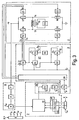
- Fig. 3 illustrates an address generator 1, a permanent memory 2, a switching-pulse generator 3, a switching circuit 4, and a unit 5 for generating timing signals with a wide application of digital techniques.
- the address generator 1 produces addresses at frequency f W . These addresses are used to assign information in memory 2 concerning the pulse width (p) of the switching pulses to be generated in switching pulse generator 3. Since in the case in question high-power switching pulses must be generated in switching circuit 4 and, in view of space and economy, an accumulator of minimum size must be used, the supply voltage delivered by the accumulator will drop considerably during the generation process. This will occur to a greater extent as the width of the switching pulses to be generated is greater and, hence, the power from the accumulator is drawn over a longer period.
- the pulse width values required in the second half of the transmission pulse generation cycle must be somewhat greater than those arranged in a mirror-image relationship in the first half of the cycle.
- pulse-width error generator 6 which is connected to the supply voltage V of the switching circuit 4 and which delivers the information to be gathered about the variation of this voltage to the permanent memory 2.
- This information combined with that of address generator 1 gives an insight into the pulse width information to be selected to obtain a transmission pulse with a symmetrical waveform from switching circuit 4.
- a feasible embodiment of pulse-width error generator 6 comprises a voltage sensor 7 connected to the supply voltage V, an A/D converter 8 connected to sensor 7, and a register 9 connected to A/D converter 8. Each time interval, in which two consecutive switching pulses are produced at a frequency f w , the information obtained with A/D converter 8 is written into register 9 for subsequent storage into memory 2.
- unit 5 is designed to generate timing signals pertaining to frequencies fp and f W .
- Memory 2 thereto comprises a main memory 10 and an assembly of submemories 11A-M corresponding with the number of transmitting frequencies fW.
- Address generator 1 selects the desired submemory in accordance with the nature of the frequency selection information Y.
- the submemory selected delivers the standard pulse width information pertaining to these addresses to the main memory 10.
- the supply of both the standard pulse width information and the aforementioned voltage amplitude information to main memory 10 results in the delivery of corrected pulse width information concerning the transmission pulse from memory 10 to the switching pulse generator 3.
- the transmission pulse is generated in accordance with the corrected digital pulse width information and with the aid of counting circuits incorporated in switching pulse generator 3, the period T w pertaining to transmitting frequency f w is divided into a suitable number of time increments T s (see Fig. 1 B); the clock pulses t s (to be generated at frequency f s ) corresponding with the time increments are supplied by unit 5.
- the corrected pulse width information from memory 2 is therefore relative to time increments T se' in which the switching pulse will commence, and to time increments T S1 in which this pulse will terminate.
- switching circuit 4 is activated with each switching pulse to derive the transmission signal of Fig. 2 from the inductive load 12 in the switching circuit.
- the switching circuit 4 in Fig. 3 is provided with two parallel circuits 13 and 14 connected to the supply voltage V, each of which circuits consisting of a pair of series-connected power transistors 15, 16 and 17, 18 respectively.
- Each of these power transistors is driven by a base control element 19, 20, 21 and 22 respectively, receiving the required control signals from the switching pulse generator 3.
- the center parts of circuits 13 and 14 are bridged by inductive load 12, which comprises a filter circuit 23 with an ultrasonic transducer at the secondary side.
- Such switching of the power transistors 15-18 requires that a power transistor 16 or 18 operating at the lower voltage level is cut off at least during the period in which power transistor 15 or 17 operating at the higher voltage level and in the same parallel circuit, is conducting to prevent a short circuit occurring in switching circuit 4.
- a switching program in which a transistor 15 or 17 operating at the higher voltage level is switched to the conducting state and the adjacent transistor 16 or 18 operating at the lower voltage level to the cut-off state at the same time, because the switching of transistor 16 or 18 to the cut-off state is slower than the switching of transistor 16 or 18 to the conducting state.
- transistor 16 or 17 operating at the lower voltage level should already be in the cut-off state.
- an induction voltage will be built up across the primary winding. If no measures are taken, this voltage will cause damage to transistor 16 or 18 respectively connected to transistor 15 or 17 to be cut off.
- the first measure consists in maintaining the cut-off state of transistor 16 or 18, operating at the lower voltage level, for some time after the adjacent transistor 15 or 17 operating at the higher voltage level has been cut off; the second measure consists in the use of a diode.
- the memory 2 also comprises a reference pulse circuit 25 connected to the main memory 10, while the switching pulse generator 3 is provided with a switch 26 connected to circuit 25 and a first and a second pulse shaping network 27 and 28 connected to switch 26.
- the main memory 10 supplies the digital standard pulse width information.
- the reference pulse circuit 25 With this information the reference pulse circuit 25 generates a "reference" pulse I r , situated asymmetrical within the pertaining time interval ( T W ) determined by two timing signals T W .
- a feasible embodiment of such a reference pulse circuit 25 is obtained with a combination of a subtracting unit 29 and an adding unit 30.
- the subtracting unit 29 stores the half value of the standard width information (n-p) at the start of the above time interval T W
- the adding unit 30 stores the full value (n-p), where n is the number of clock pulse intervals corresponding with one switching pulse period and p the specific pulse width expressed in the number of clock pulse intervals.
- the subtracting unit 29 is activated to count down to zero at the start of the interval 2 T W
- the adding unit 30 counting up to n is activated by the subtracting unit 29 after reaching zero. When the subtracting unit 29 reaches zero the leading edge of pulse I, appears.
- Both units 29 and 30 are driven by increment pulses T s from the timing unit 5.
- Switch 26 controlled with the timing signals T W is used to activate the first and the second pulse shaping networks 27 and 28 alternately, such that in one time interval the control signals to be generated are received and processed by power transistors 15 and 16 and in the following time interval by the other two power transistors 17 and 18. Since the two networks 27 and 28 are similar, only the first pulse shaping network 27 will be described, making reference to Figs. 4A-G.
- Fig. 4A illustrates a timing diagram of a reference pulse I r with a pulse width p specified in the standard pulse width information, as generated by the reference pulse circuit 25 within the time intervals determined by the timing signals T W1 and T W2 .
- the reference pulse I r is used to obtain a control pulse for the power transistor 15, operating at the higher voltage level, and a control pulse for the adjacent power transistor 16, operating at the lower voltage level, where the latter control pulse is initiated a certain period T earlier, and may continue for a corresponding period T longer than the former control pulse.
- the first network 27 comprises a first starting element 31, a second starting element 32, a first counter 33, a second counter 34, a register 35 and a logic circuit 36.
- the first starting element 31 On receiving the leading edge of reference pulse I r (see Flg. 4A) from the reference pulse circuit 25 via switch 26, the first starting element 31 will deliver a starting signal for generating of pulse I L by the first counter 33.
- Counter 33 stores a given digital number representing a certain period T from register 35 (see Fig. 4B).
- the leading edge of the starting signal is aiso determinative for the start of the generation of the control signal I c in logic circuit 36 for the other transistor 16 (see Fig. 4D).
- this counter stops and delivers a switching signal to the logic circuit 36. This moment is determinative for the occurrence of the leading edge of the control pulse Is of Fig.
- the logic circuit 36 comprises two separate outputs connected to the base control element 19, which consists of an inductive transmission circuit (not shown in the figure) with a double primary winding, energised separately by the signals (I k , I H ) generated at the separate outputs of the logic circuit 36.
- the power transistor 15 On the leading edge of the signal I K (see Fig. 4F) initiated with the leading edge of pulse Is of Fig. 4E and appearing at one output of circuit 36, the power transistor 15 will start conducting through one of the primary circuits, and on the leading edge of the signal I H (see Fig. 4G) initiated by the trailing edge of pulse Is of Fig. 4E and appearing at the other output, this transistor will be cut off through the other primary circuit.
- the arrangement described above enables to generate an ultrasonic transmission signal "having an accurately defined amplitude modulation pattern.
- Such an arrangement is ideally suited to generate an ultrasonic transmission pulse with a negligibly low side-lobe level, using preestablished standard pulse width information, which is later adaptable with the pulse-width error generator 6: this creates better possibilities to determine a doppler frequency in an echo signal from an object moving in water.
- a transmission pulse of such characteristics reference is made to a pulse of an amplitude behaviour characterised by the so- called Hamming function: where A, B, c and d are suitably selected constants.
- the arrangement shown in this figure comprises a number of power amplifiers 37A-N, to which a corresponding number of transducers 38A-N are connected separately; these transducers are arranged in a circle.
- Each of the power amplifiers 37A-N consists of a switching pulse generator 3 and a switching circuit 4, as described with reference to Fig. 3.
- This arrangement further comprises a memory 2 of which the operation has already been described with reference to Fig. 3.
- transducers 38B-G To generate a plane wave at an angle ⁇ with respect to a fixed reference line R (see Fig. 5), the six transducers 38B-G are oriented in a direction which corresponds nearest with the direction of propagation of the plane wavefront. Transducers 38B-G have an identical program for the generation of switching pulses, as described with reference to Figs. lA-B, 2 and 4A-G, but these six switching programs are not completed in phase.
- a first number of memory cells of the delay line will be filled for example with the binary number 0, then with the binary number 1 for a period corresponding with the pulse width p, and again with the binary number 0 for the remaining period T W . Since delay lines 39a-f are identical to each other, only delay line 39a will be described.
- Delay line 39a comprises a shift register 40, of which the word length is determined by the number of time increments T s during a period T W .
- Shift register 40 contains the reference pulse in binary form.
- Delay line 39a further comprises a write pulse generator 41, a register 42 and a read pulse generator 43.
- the write pulse generator 41 generates a write pulse, which ensures that, on the application to shift register 40, the binary reference pulse required for a following period T W is transferred from memory 2 into the shift register 40.
- This write pulse is also applied to register 42, which in response delivers to the read pulse generator 43 a digital number representing the required delay. After count-down of this digital number in generator 43, this generator delivers a read pulse to the shift register 40 to shift the binary information on the pulse shape out of shift register 40.
- a selection circuit 44 is incorporated between the six delay lines 39a-f and the power amplifiers 37A-N. With the given angle ⁇ the selection circuit 44 connects the six power amplifiers 37B-G, separately to delay lines 39a-f to transmit the plane wavefront at an angle ⁇ with respect to the reference line R.
Landscapes
- Engineering & Computer Science (AREA)
- Physics & Mathematics (AREA)
- General Physics & Mathematics (AREA)
- Theoretical Computer Science (AREA)
- Computer Networks & Wireless Communication (AREA)
- Radar, Positioning & Navigation (AREA)
- Remote Sensing (AREA)
- General Engineering & Computer Science (AREA)
- Acoustics & Sound (AREA)
- Multimedia (AREA)
- Ultra Sonic Daignosis Equipment (AREA)
- Measurement Of Velocity Or Position Using Acoustic Or Ultrasonic Waves (AREA)
- Amplitude Modulation (AREA)
- Electrophonic Musical Instruments (AREA)
- Investigating Or Analyzing Materials By The Use Of Ultrasonic Waves (AREA)
Abstract
Description
- The invention relates to an arrangement for generating amplitude-modulated, ultrasonic transmission pulses, which arrangement is provided with a switching circuit controlled with a plurality of switching pulses per transmission pulse interval, which switching circuit includes an inductive load circuit for generating the transmission pulses and with a unit for generating timing signals determining the switching pulse frequency.
- An arrangement of this type is used preferably for generating transmission pulses with a small frequency spectrum and, in particular, with a low side-lobe level in order to achieve better detection of doppler-shifted echo signals.
- Such an arrangement is known from the U.S. patent 3,806,862 using an overdriven class B amplifier, connected to a high-power, fixed- frequency oscillator and incorporated with an amplitude modulator to obtain amplitude modulation of the oscillator output voltage. This arrangement has the disadvantage that it becomes complicated and costly if it is required to generate high power, ultrasonic transmission pulses in accordance with a predetermined amplitude behaviour with sufficient accuracy.
- It is an object of the present invention, therefore, to provide an arrangement as set forth in the opening paragraph, whereby the above disadvantage is substantially obviated.
- According to the invention, the arrangement for generating ;amplitude-modu lated, ultrasonic transmission pulses comprises a combination of:
- a. a memory, of which the memory locations are filled with the information, required per transmission pulse interval, about the pulse width of the switching pulses to be generated, which information is derived from the desired amplitude pattern of the transmission pulses to be generated;
- b. A switching-pulse generator for producing the switching pulses, using the timing signals on the one hand and the pulse width information in the memory on the other hand;
- c. an address generator for generating addresses on the supply of the timing signals to read out the memory.
- The invention will now be described with reference to the accompanying five figures of which:
- Fig. 1A is a timing diagram of a limited number of pulsed signals of varying width to obtain an amplitude-modulated ultrasonic transmission pulse, while
- Fig. 1B is a fragment of the timing diagram of Fig. 1A;
- Fig. 2 is a timing diagram of an ultrasonic transmission pulse, whose amplitude is governed by the pulsed signals shown in Fig. 1A;
- Fig. 3 is a block diagram of an arrangement for generating amplitude-modulated ultrasonic transmission pulses according to the invention;
- Figs. 4A―G are a number of timing diagrams for illustrating the active state of various units forming part of the switching-pulse generator to obtain switching pulses for the switching circuit; and
- Fig. 5 is a block diagram of a combination of arrangements for generating amplitude-modulated ultrasonic transmission pulses according to the invention to obtain a transmission pulse having a defined wavefront.
- The timing diagram of Fig. 1 A shows a sequence of pulsed signals generated at a given switch pulse frequency fp, while each pair of pulses has the same pulse width (p) with an alternating polarity. Apart from such a pulse width behaviour, the pulse width (p) increases in time to a given value and subsequently decreases. When a sequence of signals of this sort is applied to an inductive load circuit of suitable dimensions, it will produce as signal component the first subharmonic of this sequence, the characteristics of which harmonic being illustrated in Fig. 2. This figure shows an amplitude-modulated signal, of which the frequency fw, being also the transmitting frequency, is given by the relationship: fw = yfp. The amplitude of this signal depends on the pulse width (p) of the pulsed signal in relation therewith and can be calculated by the Fourier method of analysis. For a desired amplitude behaviour of the abovementioned signal component it is thus possible to calculate the appurtenant pulse widths of the sequence of pulsed signals to be generated.
- An arrangement which stores information on calculated values of pulse width (p) and generates a sequence of pulsed signals to obtain an amplitude-modulated, ultrasonic transmission pulse will now be described with reference to Figs. 3 and 4A--G.
- Fig. 3 illustrates an
address generator 1, apermanent memory 2, a switching-pulse generator 3, aswitching circuit 4, and aunit 5 for generating timing signals with a wide application of digital techniques. - The
address generator 1 produces addresses at frequency fW. These addresses are used to assign information inmemory 2 concerning the pulse width (p) of the switching pulses to be generated in switchingpulse generator 3. Since in the case in question high-power switching pulses must be generated in switchingcircuit 4 and, in view of space and economy, an accumulator of minimum size must be used, the supply voltage delivered by the accumulator will drop considerably during the generation process. This will occur to a greater extent as the width of the switching pulses to be generated is greater and, hence, the power from the accumulator is drawn over a longer period. If now an amplitude-modulated ultrasonic transmission pulse with a symmetrical waveform is desired and the series of pulse-width values to be produced in the first and second halves of the generation cycle are mirror images of each other, the decrease in the supply voltage, especially during the second half of the generation cycle of the switching pulse will cause an asymmetric amplitude behaviour of the transmission pulse. To prevent that the amplitude behaviour of the symmetrically generated transmission pulse be affected by the drop in the supply voltage, the pulse width values required in the second half of the transmission pulse generation cycle must be somewhat greater than those arranged in a mirror-image relationship in the first half of the cycle. It is therefore of great advantage to provide the arrangement for generating amplitude-modulated, ultrasonic transmission pulses with a pulse-width error generator 6, which is connected to the supply voltage V of theswitching circuit 4 and which delivers the information to be gathered about the variation of this voltage to thepermanent memory 2. This information combined with that ofaddress generator 1 gives an insight into the pulse width information to be selected to obtain a transmission pulse with a symmetrical waveform fromswitching circuit 4. A feasible embodiment of pulse-width error generator 6 comprises avoltage sensor 7 connected to the supply voltage V, an A/D converter 8 connected tosensor 7, and aregister 9 connected to A/D converter 8. Each time interval, in which two consecutive switching pulses are produced at a frequency fw, the information obtained with A/D converter 8 is written intoregister 9 for subsequent storage intomemory 2. - Further, with the arrangement of Fig. 3 a choice can be made from several (m) transmitting frequencies fW, using the frequency selection information Y applied to
address generator 1. For thispurpose unit 5 is designed to generate timing signals pertaining to frequencies fp and fW.Memory 2 thereto comprises amain memory 10 and an assembly ofsubmemories 11A-M corresponding with the number of transmitting frequencies fW.Address generator 1 selects the desired submemory in accordance with the nature of the frequency selection information Y. On the supply of addresses fromaddress generator 1, the submemory selected delivers the standard pulse width information pertaining to these addresses to themain memory 10. The supply of both the standard pulse width information and the aforementioned voltage amplitude information tomain memory 10 results in the delivery of corrected pulse width information concerning the transmission pulse frommemory 10 to the switchingpulse generator 3. - Since the transmission pulse is generated in accordance with the corrected digital pulse width information and with the aid of counting circuits incorporated in switching
pulse generator 3, the period T w pertaining to transmitting frequency fw is divided into a suitable number of time increments Ts (see Fig. 1 B); the clock pulses ts (to be generated at frequency fs) corresponding with the time increments are supplied byunit 5. The corrected pulse width information frommemory 2 is therefore relative to time increments Tse' in which the switching pulse will commence, and to time increments T S1 in which this pulse will terminate. - Using a sequence of suitably selected switching pulses generated following this principle,
switching circuit 4 is activated with each switching pulse to derive the transmission signal of Fig. 2 from theinductive load 12 in the switching circuit. For this purpose theswitching circuit 4 in Fig. 3 is provided with twoparallel circuits power transistors base control element switching pulse generator 3. Further, the center parts ofcircuits inductive load 12, which comprises afilter circuit 23 with an ultrasonic transducer at the secondary side. Twotransistors different circuits transistors inductive load 12 ofswitching circuit 4. - Such switching of the power transistors 15-18 however requires that a
power transistor switching circuit 4. However, it is difficult to realise a switching program in which a transistor 15 or 17 operating at the higher voltage level is switched to the conducting state and theadjacent transistor transistor transistor transistor 16 or 17 operating at the lower voltage level should already be in the cut-off state. Further, when power transitor 15 or 17 operating at the higher voltage level is cut off, an induction voltage will be built up across the primary winding. If no measures are taken, this voltage will cause damage totransistor transistor transistor - The switching of two interconnected
transistors transistor memory 2 also comprises areference pulse circuit 25 connected to themain memory 10, while theswitching pulse generator 3 is provided with aswitch 26 connected tocircuit 25 and a first and a secondpulse shaping network switch 26. As already stated, themain memory 10 supplies the digital standard pulse width information. With this information thereference pulse circuit 25 generates a "reference" pulse Ir, situated asymmetrical within the pertaining time interval (TW) determined by two timing signals TW. A feasible embodiment of such a
reference pulse circuit 25 is obtained with a combination of a subtractingunit 29 and an addingunit 30. The subtractingunit 29 stores the half value of the standard width information (n-p) at the start of the above time interval
unit 30 stores the full value (n-p), where n is the number of clock pulse intervals corresponding with one switching pulse period and p the specific pulse width expressed in the number of clock pulse intervals. The subtractingunit 29 is activated to count down to zero at the start of the interval
unit 30 counting up to n is activated by the subtractingunit 29 after reaching zero. When the subtractingunit 29 reaches zero the leading edge of pulse I, appears. If then the addingunit 30 reaches its full value the trailing edge of the pulse I, appears. Bothunits timing unit 5.Switch 26 controlled with the timing signals TW is used to activate the first and the secondpulse shaping networks power transistors 15 and 16 and in the following time interval by the other twopower transistors 17 and 18. Since the twonetworks pulse shaping network 27 will be described, making reference to Figs. 4A-G. - Fig. 4A illustrates a timing diagram of a reference pulse Ir with a pulse width p specified in the standard pulse width information, as generated by the
reference pulse circuit 25 within the time intervals determined by the timing signals TW1 and TW2. The reference pulse Ir is used to obtain a control pulse for the power transistor 15, operating at the higher voltage level, and a control pulse for theadjacent power transistor 16, operating at the lower voltage level, where the latter control pulse is initiated a certain period T earlier, and may continue for a corresponding period T longer than the former control pulse. To obtain such control pulses, thefirst network 27 comprises afirst starting element 31, asecond starting element 32, afirst counter 33, asecond counter 34, aregister 35 and alogic circuit 36. - On receiving the leading edge of reference pulse Ir (see Flg. 4A) from the
reference pulse circuit 25 viaswitch 26, the first startingelement 31 will deliver a starting signal for generating of pulse IL by thefirst counter 33.Counter 33 stores a given digital number representing a certain period T from register 35 (see Fig. 4B). The leading edge of the starting signal is aiso determinative for the start of the generation of the control signal Ic inlogic circuit 36 for the other transistor 16 (see Fig. 4D). As soon ascounter 33 has decreased to zero (see pulse IL of Fig. 4B), this counter stops and delivers a switching signal to thelogic circuit 36. This moment is determinative for the occurrence of the leading edge of the control pulse Is of Fig. 4E, which activates transistor 15 by generating pulse IK of Fig. 4F. On receiving the trailing edge of the same reference pulse I, (see Fig. 4A), thesecond starting element 32 will deliver a start signal to the second counter 34 (see pulse IT of Fig. 4C), which also stored the number representing the period T fromregister 35. At theinstant counter 34 has decreased to zero (see pulse IT of Fig. 4C), this counter stops and delivers a switching signal to the first startingelement 31. Startingelement 31 reactivates counter 33 (see pulse Ie of Fig. 4B), in which again the number representing the time interval T fromregister 35 is stored. The instant at which thefirst counter 33 is activated for the second time (see pulse Ie of Fig. 4B) is also the instant at which the control pulse Is for transistor 15, operating at the higher voltage level, is to be terminated (see Fig. 4E). The moment when thefirst counter 33 has again decreased to zero (see pulse Ie of Fig. 4B) is determinative for terminating the generation of the control signal for the other transistor 16 (see pulse Ic of Fig. 4D). To obtain the active state of power transistor 15 according to Fig. 4E, thelogic circuit 36 comprises two separate outputs connected to the base control element 19, which consists of an inductive transmission circuit (not shown in the figure) with a double primary winding, energised separately by the signals (Ik, IH) generated at the separate outputs of thelogic circuit 36. On the leading edge of the signal IK (see Fig. 4F) initiated with the leading edge of pulse Is of Fig. 4E and appearing at one output ofcircuit 36, the power transistor 15 will start conducting through one of the primary circuits, and on the leading edge of the signal IH (see Fig. 4G) initiated by the trailing edge of pulse Is of Fig. 4E and appearing at the other output, this transistor will be cut off through the other primary circuit. The arrangement described above enables to generate an ultrasonic transmission signal "having an accurately defined amplitude modulation pattern. - Such an arrangement is ideally suited to generate an ultrasonic transmission pulse with a negligibly low side-lobe level, using preestablished standard pulse width information, which is later adaptable with the pulse-width error generator 6: this creates better possibilities to determine a doppler frequency in an echo signal from an object moving in water. For an example of a transmission pulse of such characteristics, reference is made to a pulse of an amplitude behaviour characterised by the so- called Hamming function:

- Furthermore, the above described method of generation of ultrasonic transmission pulses offers a suitable possibility to generate such pulses with a directed plane wavefront in accordance with the principle of interference. This will be explained with reference to Fig. 5.
- The arrangement shown in this figure comprises a number of
power amplifiers 37A-N, to which a corresponding number oftransducers 38A-N are connected separately; these transducers are arranged in a circle. Each of thepower amplifiers 37A-N consists of a switchingpulse generator 3 and aswitching circuit 4, as described with reference to Fig. 3. - This arrangement further comprises a
memory 2 of which the operation has already been described with reference to Fig. 3. - To transmit a plane wavefront in a desired direction, it is not necessary to activate all transducers; it is sufficient to use a limited number of transducers which are oriented substantially in the direction of propagation of the plane wave. This will be illustrated below in an example in which the number of transducers is limited to six. To generate a plane wave at an angle β with respect to a fixed reference line R (see Fig. 5), the six
transducers 38B-G are oriented in a direction which corresponds nearest with the direction of propagation of the plane wavefront.Transducers 38B-G have an identical program for the generation of switching pulses, as described with reference to Figs. lA-B, 2 and 4A-G, but these six switching programs are not completed in phase. Only the switching programs fortransducers 38B and 38G are carried out simultaneously, like the switching programs fortransducers transducers transducers 38B and 38G, while the switching program for 38D and 38E is again delayed with respect to that fortransducers digital delay lines 39a-f. These delay lines contain the word concerning the reference pulse for the period TW (see Fig. 1 B). Therefore, a first number of memory cells of the delay line will be filled for example with thebinary number 0, then with thebinary number 1 for a period corresponding with the pulse width p, and again with thebinary number 0 for the remaining period TW. Sincedelay lines 39a-f are identical to each other,only delay line 39a will be described. -
Delay line 39a comprises ashift register 40, of which the word length is determined by the number of time increments Ts during a period TW. Shift register 40 contains the reference pulse in binary form.Delay line 39a further comprises awrite pulse generator 41, aregister 42 and aread pulse generator 43. Thewrite pulse generator 41 generates a write pulse, which ensures that, on the application to shiftregister 40, the binary reference pulse required for a following period TW is transferred frommemory 2 into theshift register 40. This write pulse is also applied to register 42, which in response delivers to the read pulse generator 43 a digital number representing the required delay. After count-down of this digital number ingenerator 43, this generator delivers a read pulse to theshift register 40 to shift the binary information on the pulse shape out ofshift register 40. - To get the information of the six
delay lines 39a-f into the appropriate six power amplifiers, 37B-G in the case in question, aselection circuit 44 is incorporated between the sixdelay lines 39a-f and thepower amplifiers 37A-N. With the given angle β theselection circuit 44 connects the sixpower amplifiers 37B-G, separately todelay lines 39a-f to transmit the plane wavefront at an angle β with respect to the reference line R.
Claims (11)
Applications Claiming Priority (2)
| Application Number | Priority Date | Filing Date | Title |
|---|---|---|---|
| NL7808635 | 1978-08-22 | ||
| NL7808635A NL7808635A (en) | 1978-08-22 | 1978-08-22 | SONAR. |
Publications (3)
| Publication Number | Publication Date |
|---|---|
| EP0016812A1 EP0016812A1 (en) | 1980-10-15 |
| EP0016812B1 true EP0016812B1 (en) | 1983-05-11 |
| EP0016812B2 EP0016812B2 (en) | 1988-08-24 |
Family
ID=19831412
Family Applications (1)
| Application Number | Title | Priority Date | Filing Date |
|---|---|---|---|
| EP79901029A Expired EP0016812B2 (en) | 1978-08-22 | 1980-03-25 | Sonar transmitter for generating amplitude-modulated pulses |
Country Status (11)
| Country | Link |
|---|---|
| US (1) | US4347592A (en) |
| EP (1) | EP0016812B2 (en) |
| JP (1) | JPS648312B2 (en) |
| AU (1) | AU526047B2 (en) |
| BE (1) | BE878310A (en) |
| CA (1) | CA1144636A (en) |
| DE (1) | DE2965371D1 (en) |
| IT (1) | IT1120529B (en) |
| NL (1) | NL7808635A (en) |
| NO (1) | NO148867C (en) |
| WO (1) | WO1980000497A1 (en) |
Families Citing this family (9)
| Publication number | Priority date | Publication date | Assignee | Title |
|---|---|---|---|---|
| US4864547A (en) * | 1986-05-20 | 1989-09-05 | Crestek, Inc. | Regulated ultrasonic generator |
| EP0272347B1 (en) * | 1986-12-24 | 1989-06-07 | Hewlett-Packard GmbH | Method of and apparatus for adjusting the intensity profile of an ultrasound beam |
| JPS63272333A (en) * | 1987-04-30 | 1988-11-09 | Yokogawa Medical Syst Ltd | Pulse doppler ultrasonic diagnostic apparatus |
| JPH0334411U (en) * | 1989-08-11 | 1991-04-04 | ||
| EP0484565A1 (en) * | 1990-11-05 | 1992-05-13 | Siemens Aktiengesellschaft | Integral local mode control for ultrasound proximity switches |
| US5675554A (en) * | 1994-08-05 | 1997-10-07 | Acuson Corporation | Method and apparatus for transmit beamformer |
| AU3361095A (en) * | 1994-08-05 | 1996-03-04 | Acuson Corporation | Method and apparatus for transmit beamformer system |
| US5481230A (en) * | 1994-11-14 | 1996-01-02 | Tektronix, Inc. | Phase modulator having individually placed edges |
| DE102016209815A1 (en) * | 2016-06-03 | 2017-12-07 | Zf Friedrichshafen Ag | Trailer coupling and method for buckling angle detection and film sensor |
Family Cites Families (5)
| Publication number | Priority date | Publication date | Assignee | Title |
|---|---|---|---|---|
| US3243728A (en) * | 1963-06-28 | 1966-03-29 | Westinghouse Electric Corp | Sine wave generator comprising a plurality of resonant circuits discharged into a resonant load |
| US3806862A (en) * | 1969-08-26 | 1974-04-23 | Bendix Corp | Amplifier for sonar transmitter |
| DE2163053C3 (en) * | 1971-07-23 | 1979-08-02 | Fried. Krupp Gmbh, 4300 Essen | Switching arrangement for the formation of chronologically successive group signals in direction finding technology |
| US3889263A (en) * | 1973-11-15 | 1975-06-10 | Megapulse Inc | Radio-frequency pulse generation system and method |
| GB1504313A (en) * | 1974-03-11 | 1978-03-15 | Nippon Telegraph & Telephone | Inverter controlling device |
-
1978
- 1978-08-22 NL NL7808635A patent/NL7808635A/en not_active Application Discontinuation
-
1979
- 1979-08-02 WO PCT/NL1979/000003 patent/WO1980000497A1/en not_active Ceased
- 1979-08-02 DE DE7979901029T patent/DE2965371D1/en not_active Expired
- 1979-08-02 JP JP54501211A patent/JPS648312B2/ja not_active Expired
- 1979-08-02 US US06/206,193 patent/US4347592A/en not_active Expired - Lifetime
- 1979-08-17 CA CA000333995A patent/CA1144636A/en not_active Expired
- 1979-08-20 BE BE0/196784A patent/BE878310A/en not_active IP Right Cessation
- 1979-08-21 IT IT50073/79A patent/IT1120529B/en active
- 1979-08-21 NO NO792713A patent/NO148867C/en unknown
- 1979-08-21 AU AU50141/79A patent/AU526047B2/en not_active Ceased
-
1980
- 1980-03-25 EP EP79901029A patent/EP0016812B2/en not_active Expired
Also Published As
| Publication number | Publication date |
|---|---|
| NL7808635A (en) | 1980-02-26 |
| EP0016812A1 (en) | 1980-10-15 |
| US4347592A (en) | 1982-08-31 |
| WO1980000497A1 (en) | 1980-03-20 |
| AU5014179A (en) | 1980-02-28 |
| DE2965371D1 (en) | 1983-06-16 |
| JPS55500587A (en) | 1980-09-04 |
| NO148867C (en) | 1983-12-28 |
| CA1144636A (en) | 1983-04-12 |
| NO792713L (en) | 1980-02-25 |
| IT7950073A0 (en) | 1979-08-21 |
| AU526047B2 (en) | 1982-12-16 |
| JPS648312B2 (en) | 1989-02-13 |
| NO148867B (en) | 1983-09-19 |
| IT1120529B (en) | 1986-03-26 |
| EP0016812B2 (en) | 1988-08-24 |
| BE878310A (en) | 1979-12-17 |
Similar Documents
| Publication | Publication Date | Title |
|---|---|---|
| US4611494A (en) | Ultrasonic imaging apparatus using digital control | |
| EP0016812B2 (en) | Sonar transmitter for generating amplitude-modulated pulses | |
| US4023175A (en) | Imaging systems | |
| US4282452A (en) | Method and circuit arrangement for energizing ultrasonic transducers which are utilized in impulse echo technology | |
| US4870971A (en) | Transmit focus generator for ultrasound imaging | |
| JP2644849B2 (en) | FM-CW radar device | |
| GB2135547A (en) | Pulse circuits | |
| US4663746A (en) | Self-scanned time multiplexer with delay line | |
| US4020446A (en) | Ultrasonic wave transmitting system | |
| RU2108677C1 (en) | Radio noise shaping device | |
| US4276621A (en) | Object confirming apparatus | |
| CA1316250C (en) | Saw circuit for generating continuous time-coherent rf carriers | |
| US12379475B2 (en) | Ultrasonic sensor control device, ultrasonic sensor, and ultrasonic sensor control method | |
| JPH0474988A (en) | Driving of a multitude of radars and radar device | |
| RU97112753A (en) | COMMUNICATION DEVICE | |
| JPS61271485A (en) | Continuous wave transmission for multi-frequency ultrasonic pulse | |
| JPH0117551B2 (en) | ||
| JPS5924276A (en) | System for driving phased array vibrator | |
| RU538U1 (en) | Microwave Delay Line | |
| RU1676352C (en) | Parametric active sonar | |
| SU1223136A1 (en) | Apparatus for determining instant of acoustic emission signal maximum | |
| SU1763972A1 (en) | Recording device for working pieces ultrasonic testing | |
| SU1352408A1 (en) | Device for measuring amplitude and phase of signals of phased array radiators | |
| JPS59153186A (en) | Exciting of ultrasonic transducer | |
| JPS6398579A (en) | Driving of vibrator of ultrasonic sensor |
Legal Events
| Date | Code | Title | Description |
|---|---|---|---|
| PUAI | Public reference made under article 153(3) epc to a published international application that has entered the european phase |
Free format text: ORIGINAL CODE: 0009012 |
|
| AK | Designated contracting states |
Designated state(s): CH DE FR GB NL SE |
|
| 17P | Request for examination filed | ||
| GRAA | (expected) grant |
Free format text: ORIGINAL CODE: 0009210 |
|
| AK | Designated contracting states |
Designated state(s): CH DE FR GB NL SE |
|
| REF | Corresponds to: |
Ref document number: 2965371 Country of ref document: DE Date of ref document: 19830616 |
|
| ET | Fr: translation filed | ||
| PLBI | Opposition filed |
Free format text: ORIGINAL CODE: 0009260 |
|
| 26 | Opposition filed |
Opponent name: KRUPP ATLAS ELEKTRONIK GMBH Effective date: 19840207 |
|
| PUAH | Patent maintained in amended form |
Free format text: ORIGINAL CODE: 0009272 |
|
| STAA | Information on the status of an ep patent application or granted ep patent |
Free format text: STATUS: PATENT MAINTAINED AS AMENDED |
|
| 27A | Patent maintained in amended form |
Effective date: 19880824 |
|
| AK | Designated contracting states |
Kind code of ref document: B2 Designated state(s): CH DE FR GB NL SE |
|
| NLR2 | Nl: decision of opposition | ||
| ET3 | Fr: translation filed ** decision concerning opposition | ||
| NLR3 | Nl: receipt of modified translations in the netherlands language after an opposition procedure | ||
| NLT1 | Nl: modifications of names registered in virtue of documents presented to the patent office pursuant to art. 16 a, paragraph 1 |
Owner name: HASRODE B.V. TE EINDHOVEN. |
|
| NLS | Nl: assignments of ep-patents |
Owner name: HOLLANDSE SIGNAALAPPARATEN B.V. TE HENGELO (O.). |
|
| REG | Reference to a national code |
Ref country code: GB Ref legal event code: 732 |
|
| REG | Reference to a national code |
Ref country code: FR Ref legal event code: TP Ref country code: FR Ref legal event code: CD Ref country code: FR Ref legal event code: CA |
|
| REG | Reference to a national code |
Ref country code: CH Ref legal event code: PUE Owner name: HOLLANDSE SIGNAALAPPARATEN B.V. Ref country code: CH Ref legal event code: PFA Free format text: HASRODE B.V. |
|
| PGFP | Annual fee paid to national office [announced via postgrant information from national office to epo] |
Ref country code: FR Payment date: 19930715 Year of fee payment: 15 |
|
| PGFP | Annual fee paid to national office [announced via postgrant information from national office to epo] |
Ref country code: SE Payment date: 19930716 Year of fee payment: 15 |
|
| PGFP | Annual fee paid to national office [announced via postgrant information from national office to epo] |
Ref country code: CH Payment date: 19930721 Year of fee payment: 15 |
|
| PGFP | Annual fee paid to national office [announced via postgrant information from national office to epo] |
Ref country code: GB Payment date: 19930723 Year of fee payment: 15 |
|
| PGFP | Annual fee paid to national office [announced via postgrant information from national office to epo] |
Ref country code: DE Payment date: 19930817 Year of fee payment: 15 |
|
| PGFP | Annual fee paid to national office [announced via postgrant information from national office to epo] |
Ref country code: NL Payment date: 19930831 Year of fee payment: 15 |
|
| PG25 | Lapsed in a contracting state [announced via postgrant information from national office to epo] |
Ref country code: GB Effective date: 19940802 |
|
| PG25 | Lapsed in a contracting state [announced via postgrant information from national office to epo] |
Ref country code: SE Effective date: 19940803 |
|
| PG25 | Lapsed in a contracting state [announced via postgrant information from national office to epo] |
Ref country code: CH Effective date: 19940831 |
|
| EAL | Se: european patent in force in sweden |
Ref document number: 79901029.3 |
|
| PG25 | Lapsed in a contracting state [announced via postgrant information from national office to epo] |
Ref country code: NL Effective date: 19950301 |
|
| GBPC | Gb: european patent ceased through non-payment of renewal fee |
Effective date: 19940802 |
|
| NLV4 | Nl: lapsed or anulled due to non-payment of the annual fee | ||
| PG25 | Lapsed in a contracting state [announced via postgrant information from national office to epo] |
Ref country code: FR Effective date: 19950428 |
|
| REG | Reference to a national code |
Ref country code: CH Ref legal event code: PL |
|
| PG25 | Lapsed in a contracting state [announced via postgrant information from national office to epo] |
Ref country code: DE Effective date: 19950503 |
|
| EUG | Se: european patent has lapsed |
Ref document number: 79901029.3 |
|
| REG | Reference to a national code |
Ref country code: FR Ref legal event code: ST |