EP0014100B1 - Analogue display - Google Patents
Analogue display Download PDFInfo
- Publication number
- EP0014100B1 EP0014100B1 EP80300236A EP80300236A EP0014100B1 EP 0014100 B1 EP0014100 B1 EP 0014100B1 EP 80300236 A EP80300236 A EP 80300236A EP 80300236 A EP80300236 A EP 80300236A EP 0014100 B1 EP0014100 B1 EP 0014100B1
- Authority
- EP
- European Patent Office
- Prior art keywords
- electrodes
- display
- electrode
- signals
- segment
- Prior art date
- Legal status (The legal status is an assumption and is not a legal conclusion. Google has not performed a legal analysis and makes no representation as to the accuracy of the status listed.)
- Expired
Links
- 239000000463 material Substances 0.000 claims description 25
- 230000003098 cholesteric effect Effects 0.000 claims description 11
- 239000004020 conductor Substances 0.000 claims description 4
- 230000002093 peripheral effect Effects 0.000 claims description 4
- 239000004988 Nematic liquid crystal Substances 0.000 claims description 3
- 239000004973 liquid crystal related substance Substances 0.000 description 25
- 239000000975 dye Substances 0.000 description 7
- 230000000694 effects Effects 0.000 description 7
- 230000003287 optical effect Effects 0.000 description 7
- 210000004027 cell Anatomy 0.000 description 6
- 210000002858 crystal cell Anatomy 0.000 description 6
- 238000010276 construction Methods 0.000 description 5
- 239000013256 coordination polymer Substances 0.000 description 4
- 239000011248 coating agent Substances 0.000 description 3
- 238000000576 coating method Methods 0.000 description 3
- 230000000295 complement effect Effects 0.000 description 3
- 239000011521 glass Substances 0.000 description 3
- 230000000977 initiatory effect Effects 0.000 description 3
- 239000003550 marker Substances 0.000 description 3
- 239000011159 matrix material Substances 0.000 description 3
- 238000000034 method Methods 0.000 description 3
- 206010034719 Personality change Diseases 0.000 description 2
- 230000005540 biological transmission Effects 0.000 description 2
- 230000005465 channeling Effects 0.000 description 2
- 238000010586 diagram Methods 0.000 description 2
- 238000001704 evaporation Methods 0.000 description 2
- 230000008020 evaporation Effects 0.000 description 2
- 239000011810 insulating material Substances 0.000 description 2
- 239000000203 mixture Substances 0.000 description 2
- 230000002441 reversible effect Effects 0.000 description 2
- 239000007787 solid Substances 0.000 description 2
- 125000006850 spacer group Chemical group 0.000 description 2
- 239000004094 surface-active agent Substances 0.000 description 2
- XOLBLPGZBRYERU-UHFFFAOYSA-N tin dioxide Chemical compound O=[Sn]=O XOLBLPGZBRYERU-UHFFFAOYSA-N 0.000 description 2
- 229910001887 tin oxide Inorganic materials 0.000 description 2
- IIZPXYDJLKNOIY-JXPKJXOSSA-N 1-palmitoyl-2-arachidonoyl-sn-glycero-3-phosphocholine Chemical compound CCCCCCCCCCCCCCCC(=O)OC[C@H](COP([O-])(=O)OCC[N+](C)(C)C)OC(=O)CCC\C=C/C\C=C/C\C=C/C\C=C/CCCCC IIZPXYDJLKNOIY-JXPKJXOSSA-N 0.000 description 1
- 238000010521 absorption reaction Methods 0.000 description 1
- 239000004411 aluminium Substances 0.000 description 1
- 229910052782 aluminium Inorganic materials 0.000 description 1
- XAGFODPZIPBFFR-UHFFFAOYSA-N aluminium Chemical compound [Al] XAGFODPZIPBFFR-UHFFFAOYSA-N 0.000 description 1
- 239000001000 anthraquinone dye Substances 0.000 description 1
- 239000000987 azo dye Substances 0.000 description 1
- 239000003086 colorant Substances 0.000 description 1
- 239000006059 cover glass Substances 0.000 description 1
- 238000000354 decomposition reaction Methods 0.000 description 1
- 239000003989 dielectric material Substances 0.000 description 1
- 230000005684 electric field Effects 0.000 description 1
- 239000007772 electrode material Substances 0.000 description 1
- 230000007274 generation of a signal involved in cell-cell signaling Effects 0.000 description 1
- 238000005286 illumination Methods 0.000 description 1
- 230000002427 irreversible effect Effects 0.000 description 1
- 238000002955 isolation Methods 0.000 description 1
- 229940067606 lecithin Drugs 0.000 description 1
- 235000010445 lecithin Nutrition 0.000 description 1
- 239000000787 lecithin Substances 0.000 description 1
- 229910001635 magnesium fluoride Inorganic materials 0.000 description 1
- 230000000873 masking effect Effects 0.000 description 1
- 229910052751 metal Inorganic materials 0.000 description 1
- 239000002184 metal Substances 0.000 description 1
- 150000001282 organosilanes Chemical class 0.000 description 1
- 239000003973 paint Substances 0.000 description 1
- 230000000306 recurrent effect Effects 0.000 description 1
- 230000003252 repetitive effect Effects 0.000 description 1
- 238000005070 sampling Methods 0.000 description 1
- 239000004332 silver Substances 0.000 description 1
- 229910052709 silver Inorganic materials 0.000 description 1
Images


Classifications
-
- G—PHYSICS
- G01—MEASURING; TESTING
- G01R—MEASURING ELECTRIC VARIABLES; MEASURING MAGNETIC VARIABLES
- G01R13/00—Arrangements for displaying electric variables or waveforms
- G01R13/40—Arrangements for displaying electric variables or waveforms using modulation of a light beam otherwise than by mechanical displacement, e.g. by Kerr effect
- G01R13/404—Arrangements for displaying electric variables or waveforms using modulation of a light beam otherwise than by mechanical displacement, e.g. by Kerr effect for discontinuous display, i.e. display of discrete values
-
- G—PHYSICS
- G02—OPTICS
- G02F—OPTICAL DEVICES OR ARRANGEMENTS FOR THE CONTROL OF LIGHT BY MODIFICATION OF THE OPTICAL PROPERTIES OF THE MEDIA OF THE ELEMENTS INVOLVED THEREIN; NON-LINEAR OPTICS; FREQUENCY-CHANGING OF LIGHT; OPTICAL LOGIC ELEMENTS; OPTICAL ANALOGUE/DIGITAL CONVERTERS
- G02F1/00—Devices or arrangements for the control of the intensity, colour, phase, polarisation or direction of light arriving from an independent light source, e.g. switching, gating or modulating; Non-linear optics
- G02F1/01—Devices or arrangements for the control of the intensity, colour, phase, polarisation or direction of light arriving from an independent light source, e.g. switching, gating or modulating; Non-linear optics for the control of the intensity, phase, polarisation or colour
- G02F1/13—Devices or arrangements for the control of the intensity, colour, phase, polarisation or direction of light arriving from an independent light source, e.g. switching, gating or modulating; Non-linear optics for the control of the intensity, phase, polarisation or colour based on liquid crystals, e.g. single liquid crystal display cells
- G02F1/133—Constructional arrangements; Operation of liquid crystal cells; Circuit arrangements
- G02F1/1333—Constructional arrangements; Manufacturing methods
- G02F1/1343—Electrodes
- G02F1/134309—Electrodes characterised by their geometrical arrangement
-
- G—PHYSICS
- G04—HOROLOGY
- G04G—ELECTRONIC TIME-PIECES
- G04G9/00—Visual time or date indication means
- G04G9/02—Visual time or date indication means by selecting desired characters out of a number of characters or by selecting indicating elements the position of which represent the time, e.g. by using multiplexing techniques
- G04G9/06—Visual time or date indication means by selecting desired characters out of a number of characters or by selecting indicating elements the position of which represent the time, e.g. by using multiplexing techniques using light valves, e.g. liquid crystals
- G04G9/062—Visual time or date indication means by selecting desired characters out of a number of characters or by selecting indicating elements the position of which represent the time, e.g. by using multiplexing techniques using light valves, e.g. liquid crystals using multiplexing techniques
Definitions
- This invention concerns analogue displays, for example timepieces (ie watches or clocks) and analogue meter displays having dial, arc or rectilinear scales where one or more scalar quantities are each represented by the relative position of an index against an optically contrasting background.
- timepieces ie watches or clocks
- analogue meter displays having dial, arc or rectilinear scales where one or more scalar quantities are each represented by the relative position of an index against an optically contrasting background.
- Analogue watches and analogue meter displays have typically been of either mechanical or electromechanical construction.
- An example of a display of non-mechanical construction a liquid crystal device analogue watch having a radial display format, has recently been described (cf. Conference Record of the IEEE Biennial Display Research Conference Oct 24-26, 1978, pp 59 ⁇ 61).
- a set of meander electrodes overlap two sets of segment electrodes across a liquid crystal cell and are addressed using !-duty cycle time-multiplexing to allow the simultaneous display of both hour and minute indices.
- the voltage across electrodes defining the index position in each case, is of such value above a threshold value, characteristic of the liquid crystal material, that a localised region of the liquid crystal material is switched ON and adopts a state providing optical contrast with the adjacent and remaining parts of the display where voltage differences less than but near threshold are applied. This allows the number of connections to the display to be reduced compared to the number required to make individual connection to each directly driven active area of the display.
- the finite voltage differences applied across OFF elements being generally near threshold may in certain types of liquid crystal device displays - eg cholestericnematic phase change effect cells incorporating pleochroic dyes - result in poor contrast and very slow dynamic response to changes in the electric address.
- the invention here provides an alternative approach to the construction of analogue displays.
- an analogue display comprises:-
- the display panel may be in the form of a liquid crystal cell wherein the medium is of liquid crystal material.
- This form of panel may include one or more polarisers and be adapted as a twisted nematic (Schadt-Helfrich) cell in which a thin layer of nematic liquid crystal material is contained between transparent electrode-bearing glass plates, the latter being treated by unidirectional rubbing and assembled with the directions of rubbing orthogonal or twisted to give a twisted alignment of the liquid crystal molecules of the layer.
- the electrode-bearing plates may be treated in other known manners such as by oblique evaporation of dielectric material eg. SiO or MgF 2 , to facilitate alignment.
- cholesteric material typically 1 % may be added to the nematic liquid crystal material to prevent display non-uniformity.
- cholesteric material typically 1 %
- pleochroic dye may be added, to give a coloured display and allow one or both polarisers to be omitted, as known in the art.
- this form of panel may be adapted as a cholesteric to nematic phase change cell including a thin layer of cholesteric material which is characterised by two phase states; one, the OFF state, wherein the material in the focal conic texture has the property of scattering incident light; the other, the ON state, wherein the material molecules are aligned by the electric field into the nematic phase and enable the transmission of incident light through the layer.
- a small amount of pleochroic dye may be added to the liquid crystal material to enhance contrast and viewability.
- the OFF state may alternatively be the (non-scattering) planar texture of the cholesteric.
- the display panel may be an ac electroluminescent panel wherein the medium is in the form of a solid layer of electroluminescent material.
- the display panel may be an ac plasma discharge panel wherein the medium is a suitable gas.
- the sets of electrodes may be arranged to form a circular dial, an arc, or a rectilinear, display area.
- the finite RMS voltage difference in each case is somewhat greater than the saturation voltage V sat at the mean operative temperature
- the saturation voltage of the panel is that voltage difference applied across the medium that is required to ) change the relevant optical property (eg optical transmission) of the corresponding region by 90% of the full property change possible.
- the RMS voltage difference is in each case equal to a common minimum voltage:-
- the set of signals may be of pseudo-random binary sequence waveform, each of period Tand divided into a plurality of L bits (L 5 : N), with each bit having a value logic '0' or '1', corresponding to two different levels of voltage.
- the signals may be a set of suitable Walsh function signals.
- the medium 11 may be a solid layer of electroluminescent material, as in the case of an electroluminescent display panel; or, a rarefied gas, as in the case of an AC plasma discharge panel; for the purposes of this example it is a layer of liquid crystal material.
- the display panel thus adapted, is in the form of a liquid crystal cell where the liquid crystal material is enclosed in the space between the glass plates 3, 5 by a peripheral spacer 19 of insulating material. For added rigidity there is also a central support 21, also of insulating material.
- the plates 3, 5 are spaced apart by a short distance, typically of the order of 12 pm, to allow surface effect alignment of the liquid crystal material molecules to propagate across the width of the cell.
- the electrode bearing plates 3, 5 may be assembled: after unidirectionally rubbing, or, coating the electrodes by suitable oblique evaporation; or after treatment with a surfactant, such as organo-silane or lecithin, according to the liquid crystal effect used to define the different optical states, and the alignment required for display.
- a surfactant such as organo-silane or lecithin
- the liquid crystal material is cholesteric and the plates may be treated by surfactant to give focal conic alignment.
- suitable cholesteric mixtures for such a cell are the mixtures:-
- liquid crystal cell Whilst the liquid crystal cell, so far as described above, may be viewed with back illumination, it is here shown as a reflective device and has, adjacent the back plate 5, a reflector 23 which may be a specular or diffusely reflecting metal film (eg silver, aluminium), or, a diffusely reflecting white paint, or card.
- a reflector 23 which may be a specular or diffusely reflecting metal film (eg silver, aluminium), or, a diffusely reflecting white paint, or card.
- the electrode bearing plates 3, 5 extend beyond the spacer 19 to facilitate external connection to the electrode structures 7, 9.
- Electrodes 7, 9 are now described with reference to figures 2, 3 and 4. These configurations are suited to displays operated to perform as meters requiring the simultaneous display of two index characters.
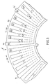
- the back electrode structure comprises ten segment portions S0, S1,... S9 arranged to form a circular array.
- Each one of the segments SO,... S9 has component parts 9a, 9b of which the parts 9a are each in the form of a shaped segment, and the part 9b is in the form of a peripheral background electrode adjacent and nearly surrounding the parts 9a.
- the electrode 9b as shown, has a number of thin outwardly extending limbs 9b', which limbs extend between the parts 9a and are isolated from them by narrow spacing.
- the limbs 9b' are integrally connected, to form the single background electrode 9b, by a central ring conductor 9b". Consequently, the whole of the display area provided by segments S0,...
- S9 is almost completely spanned by the material of the electrodes 9a, 9b with the exception of a minimum of space necessary for electrode isolation.
- the sectors 9a of the segments SO, ... S9 are connected to pad terminals T0, ... T9 respectively; and the background electrode 9b is connected to a single terminal TX by connecting strips 25 (shown schematically). Since the limbs 9b' of the background electrode 9b are connected centrally, the connections to the terminal may be made without bridging the connecting strips 25 on the back plate 5. It is noted that in the absence of central connection, 9b", the number of terminals TX would be unduly multiplied to avoid bridging.
- each segment electrode 9a has extended limbs 9a', 9a" and foreshortened limbs 9a".
- the extended limb 9a' of each sector 9a is lengthened to facilitate connection to the terminals TO,... T9.
- the shaped electrode 9a of the first segment SO provides five long hand index regions R01, R03, ... R09 and four short hand index regions R02, R04, R08 as determined by electrode overlap. (These regions are delineated in figure 3, to show this overlap, by broken outline).
- Si (i 1 to 9)
- long hand index regions Ri1, Ri3, ... Ri9, and short hand index regions Ri2, Ri4, ... R/8 are determined by corresponding electrode overlap.
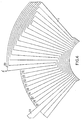
- the front electrode structure 7 comprises a set of electrodes including a first sub-set of five strip electrodes E1, E3, ... E9. These electrodes are shaped and arranged in a modified meander configuration and are registered A' upon A' to delineate the long hand index regions, eg the strip electrode E1 overlaps the segments S0, S1, ... S9 delineating the index regions R01, R19, ... R99. Similarly electrode E9 delineates the index regions R09, R11, R91. Alternating with electrodes E1, E3, ... E9 is a second sub-set of five strips electrodes E0, E2, ... E8. These electrodes overlap the short hand index regions and also the limbs 9b' of the peripheral electrode 9b.
- the strip electrode E2 overlaps the segments S0, S1, ... S9 and delineates the index regions R02, R18, ... R98.
- the strip electrode E8 similarly delineates the index regions R08, R12, ... R92.
- the electrode EO however overlaps the limbs 9b'.
- Circuitry suitable for operating the display panel 1 having the electrode configurations described, is shown in figures 5a, 5b.
- the signal generator 31 comprises a 12-bit serial-in/parallel out shift register 35 cooperative with logic feedback components 37, 39 and 41.
- the shift register 35 has twelve output ports P0, ... P11 which feed twelve signal lines L0, ... L11.
- the voltage signals on these lines change from logic'1' to logic '0' ie Hi and Lo voltage levels, respectively, (according to the logic states of the corresponding register bits), as the shift register 35 is driven by the clocking pulses of an oscillator clock CP.
- the frequency of these is ideally ⁇ 400Hz to avoid flicker.
- the voltage signals are differently phased, as ensured by the shift register.
- the first and fourth signal lines LO and L3 control the input port I of the register 35 through logic feedback components 37, 39, an exclusive OR gate, and OR gate, respectively.
- the output signals are all maintained in the Lo voltage state, so to enable code generation to begin, feedback is provided from the first four signal lines LO, ... , L3 through logic feedback component 41, a 4-input NOR gate, and the OR gate 39. This ensures that on initiation the input I is held Hi and changes the logic state of the first bit of register 35, corresponding to output port P0, line L0, from the logic '0' to the logic '1' state on the first clock edge.
- the difference between any two signals is nett Ac and has an RMS value of (8/15)1/2.
- V is the voltage difference between the Lo logic '0' and Hi logic '1' levels. It is preferable that all finite RMS voltage differences developed across the panel are greater than 1.1 times the saturation voltage characteristic of the liquid crystal material 11.
- the signals on signal lines LO, ... , L10 lay be applied directly to the input terminals TO to T9 and TX of the back plate electrode structure 9. However, if the RMS differences were not compatible, the signals on lines L0, L10 could be applied to terminals TO to T9 and TX via matching amplifiers.
- the signal selector 33 comprises two 10:1 multplexers 43A, 43B, a first set of five 2:1 multiplexers 51, ... 55 and, a second set of four 2:1 multiplexers 61, ... , 64.
- Each of the 10:1 multiplexers 43A, 438 has ten signal inputs 10, ... , 19 one connected to each of the signal lines Lo, ... , L9.
- Each 10:1 multiplexer 43A, 43B has four primary control inputs a to d and has a single output port 0. For each binary address 0 to 9 applied to the control inputs a to d, inputs 10 to 19 are connected respectively to the output port 0.
- the 10:1 multiplexer 43A and the first set of 2:1 multiplexers 51 to 55 are dedicated to the display of one of the two index characters (ie the long hand) and similarly the 10:1 multiplexers 438 and the second set of 2:1 multiplexers 61 to 64 are dedicated to the display of the other distinctive index character (ie the short hand).
- Each of the 10:1 multiplexers 43A, 43B is responsive to primary data signals which may be applied to their control inputs a to d. Each has the function of selecting, according to the primary data signal coding, one of the ten signals applied on lines LO to L9 and channeling each selected signal to each output port O.
- Each 2:1 multiplexer 51 to 55, 61 to 64 has a first and second signal input port 10',11' and an output port 0'.
- the 2:1 multiplexers 51 to 55 have each a secondary control input e to i, and the 2:1 multiplexers 61 to 64, secondary control inputs e to h. If the secondary control input is at logic "1" then the output port O' is connected to 11, and if at logic "O" then the output port is connected to 10'.
- the output ports 0' of the 2:1 multiplexers 51 to 55 are connected either directly, or, if necessary, via matching amplifiers, to the front- plate electrodes E1, E3, ...
- the first signal input ports 11' of 2:1 multiplexers 51 to 55 are connected in parallel to the output port 0 of the 10:1 multiplexer 43A, and in like manner the first signal input ports 11' of 2:1 multiplexers 61 to 64 are connected to the output port 0 of the 10:1 multiplexer 43B.
- the first set of 2:1 multiplexers 51 to 55 are responsive to secondary control signals which may be supplied to their control inputs e to i. Collectively these 2:1 multiplexers have the function of channeling the selective signal from the output port O of the 10:1 multiplexer 43A onto a selected one of the front plate electrodes E1, E3 to E9 according to the secondary control signal coding. In this way, therefore, an applied signal may be selected and channeled to a selected one of the meander electrodes E1, E3 to E9 so that across the region of the medium 11 of the display panel 1 delineated by the intersection of the selected meander electrode and the segment electrode to which this selected signal is also applied, a zero RMS difference voltage is developed since like signals are applied to the selected meander electrode and the appropriate segment electrode. The medium 11 in this delineated region is thus held in the OFF state for the duration of these like signals.
- the second set of 2:1 multiplexers 61 to 64 function in similar manner to channel the selected signal from the output port 0 of the 10:1 multiplexer 43B onto a selected one of the second subset of front plate electrodes E2, E4, E6 and E8 to produce the OFF state in another region of the medium 11.
- the second signal inputs 10' of the 2:1 multiplexers 51 to 55, and 61 to 64 are connected in parallel to signal line L11. These multiplexers ensure that the signal on this line is channeled directly, or where appropriate through amplifiers, to the remaining-and-non-selected meander electrodes E1 to E9.
- the meander electrode EO is connected directly, or through a matching amplifier, to line L11.
- the voltage signal on line L1 1 is different from all signals applied to the terminals TO to T9 and TX and consequently across all other regions of the medium 11 delineated by the overlap of the front and back-plate electrode structures 7, 9 a finite RMS voltage difference is developed and these regions, which provide the display background, are held in the ON state for the duration of these different signals. Consequently, the two distinctive index characters are displayed simultaneously against an optically contrasting background.
- FIG. 5b There are shown in figure 5b the component parts of a control data source for providing the primary and secondary control data signals to operate the signal selector 33.
- This source comprises: an input transducer 80; an A-D converter 81 including timing circuits and sampling means (not shown) where necessary; two pairs of 1:5 demultimplexers: pair 83A and 83B, and pair 85A and 85B each with an associated inverting amplifier 84, 86 respectively; and nine OR gates 91 to 99, two of these 92, 98 being 3-input OR gates.
- the input transducer 80 provides an analogue signal as an electrical measure of some scalar function (eg pressure) and this signal is coded by A-D converter 81 to produce logic signals in a binary-coded- decimal (BCD) form at three sets of four outputs a to d corresponding the binary coded units (1's), tens (10's) and hundreds (100's) of the digitised analogue values, a being the most significant, and d the least significant bit outputs.
- BCD binary-coded- decimal
- the outputs a to d corresponding to the tens and hundreds provide the primary control data signals for the 10:1 multiplexers 43A, 43B respectively.
- the first pair of 1:5 multiplexers 83A, 83B is controlled by the three most significant bit outputs of the units section of the convertor 81.
- the least significant bit output d of the next adjacent section, the tens section provides a logic signal '0' or '1' at the input port of 1:5 demultiplexer 83A to which it is connected directly, and an inverted logic signal '1' or '0' at the input port of 1:5 demultiplexer 83B to which it is connected via inverting amplifier 84.
- This pair of 1:5 demultiplexers 83A, 83B provides the secondary control data signals that control the first set of 2:1 multiplexers 51 to 55.
- a logic '1' signal is fed onto one of the five output channels a0 to a4 of the demultiplexer 83B or one of the five output channels a5 to a9 of the demultiplexer 83A, all of the other outputs being simultaneously at logic '0'. All the output channels are connected to the inputs of the OR gates 91, 93, ... , 99, which in turn have outputs connected to the control inputs e to i of the first set of 2:1 multiplexers 51 to 55.
- the output channels-ao to a9 are connected to the OR gates, 91, 93, ...
- the 1:5 multiplexers 85A, 85B are both controlled by the three most significant bit outputs of the tens section of the convertor 81.
- the least significant bit output d of the hundreds section provides logic signals '1' or '0' to demultiplexers 85A, 85B in manner similar to that above and a logic '1' is fed onto one of the control inputs e to h of the second set of multiplexers 61 to 64 after being channelled onto one of the ten output channels 60 to b9 of demultiplexers 85B, 85A and through one of the OR gates 92, 94, 96 or 98.
- These output channels b0 to b9 are connected to the OR gates 92, 94, 96 and 98 in order:- b3, b4 and b5 to 98; b2, b6 to 96; b1, b7 to 94 and b0, b8 and b9 to 92.
- the 3-input OR gates 92, 98 are connected in this manner so that it is possible to "mark time" once for every hundreds value, there being four rather than five short-hand character index positions for each segment.
- control data source with the signal selector 33, signal generator 31 and display panel 1 provides a meter display whereby values between 0 and 998 may be represented by a short-hand index character indicating the hundreds value, and the long-hand index character indicating the tens and units value of the measured scalar function.
- this meter display may be illustrated by considering the response of the display to a slowly increasing scalar function, the BCD data running in unit increments from zero.
- the three sets of four bit outputs a to d of the convertor 81 are in the 0000 condition.
- the outputs of inverting amplifiers 84, 86 are set at logic level '1' and in response the outputs on channels a0, b0 of the demultiplexers 83B, 85B are held at logic level '1'. All other demultiplexer outputs a1 to a9, and b1 to b9 are set at logic level '0'.
- a logic level '1' is thus applied via gates 91, and 92 to the controlling inputs e of the 2:1 multiplexers 51, 61 and front-plate electrodes E1, E2 are thereby selected for application of the particular drive signals selected by the two 10:1 multiplexers 43A, 43B.
- Both these 10:1 multiplexers 43A, 43B receive 0000 primary control data addresses from the tens and units BCD outputs a to d of convertor 81.
- the voltage signal on the first line LO from shift register 35 which is applied via terminal TO to segment S0, is also channeled to the frontplate electrodes E1, E2.
- the medium 11 is held in the OFF state, there being zero RMS voltage difference applied across the panel 1 since the like signals are applied to these particular overlapping electrodes.
- the liquid crystal material is maintained in the cholesteric phase (OFF state) and absorbs incident light.
- the medium 11 Since finite RMS voltage differences are applied across all other index regions R03 to R99, the medium 11 is held in the ON state and in the case of the liquid crystal cell above, the liquid crystal material is switched to, and maintained in, the nematic phase (ON state) where the dye absorption is greatly reduced, incident light being reflected from the reflector in these regions.
- a long-hand index character is displayed to indicate the 00 on the scale 15 with the short hand index character displayed in the immediately adjacent index position, both in optical contrast against the background of the display.
- the units data Upon the first increment of the BCD data, the units data changes from 0000 to 0001, the tens and hundreds data remaining unchanged. This change however produces no response since the first pair of demultiplexers 83A, 83B only responds to changes in the three most significant bits of the units data. But on the next BCD data increment, where the units data changes to 0010, the Iogic'1' level signal is switched by demultiplexers 83B from channel aO to channel a1 and in consequence, the signal on line LO is switched from electrode E1 to electrode E3 and the position of the displayed long-hand index character is changed from region R01 to R03 to indicate 02 on the graduated scale 15.
- the particular voltage signal selected by multiplexer 43A is thus applied to back-plate electrode E9.
- the primary control data address of this multiplexer 43A has been changed from 0000 to 0001 and, therefore, it is the signal on line L1, applied to terminal T1 and segment S1, that is selected.
- the long-hand index character thus changes to the position of region R11 delineated by the overlap of the back-plate electrode E9 and the front plate electrode segment S1.
- the signal on line L1 is channeled to electrodes E7, E5, E3, E1, ie the electrodes taken in reverse order, and the long-hand index character changes position from region R11 to regions R13, R15, R17, R19 to indicate values 12, 14, 16, 18 respectively on the graduated scale 15.
- the units data state is reset to 0000 and the tens data state changes from 0001 to 0010.
- These changes have three effects. Firstly, to change control from demultiplexer 83A back to 83B again so that a logic T level signal is applied to control the secondary control input e of multiplexer 51 to select back-plate electrode E1. Secondly, to change the signal selected by multiplexer 43A, to the signal on line L2, so that the long-hand index character moves from the position of region R19 to the position of region R21 to indicate a value 20 on the graduated scale 15.
- the short hand index character thus "marks time” for yet a further twenty increments, until the hundreds data state changes from 0000 to 0001 and both the tens and units data states are reset to 0000.
- the long-hand index character returns to the position of the region R01 having made a full revolution of the dial.
- the short-hand index character moves into the second segment S1 to the position of region R12.
- the circuitry of figure 5a may be simplified quite readily to provide only tens and units meter indication, ie the analogue display may be simplified for display of a single index character. Since in this simplified form of the display, hundreds indication by the short-hand index character is not required, the 10:1 multiplexer 43B and its associated set of 2:1 multiplexers 61 to 64 may be omitted. To maintain the short-hand index regions of the display in the ON state so to afford overall a contrasting background, the front-plate electrodes E2, E4, E6 and E8 with EO are connected in parallel to line L11 of the shift register and as shown in broken outline in figure 5a.
- the configuration of the back plate electrode structure 9 is shown in outline in figure 6.
- the structure is divided into twelve segment electrodes SO to S11, and a common complementary electrode 9x.
- Each segment electrode is of complex shape, as shown in figure 7, and in combination with the front plate structure 7 in Figure 8, defines, at these regions of overlap, five seconds (s), five minutes (m), and five hours (h), index character regions having marker, long-hand and, short hand shapes, respectively.
- the segment electrode is shaped to define these regions in the orders s m h s h m s m h s h m m h; whilst for the odd segments S1, S3, ...
- the segment electrode is shaped to define these regions in the reverse order s h m s m h s h m s m h s h m. It is noted that the seconds marker regions (s) are spaced evenly on an arcuate strip 9a whilst the minute and hour character regions (m) and (h), respectively, alternate about these seconds marker regions (s).
- This complex configuration allows access from the inside of the circle to the spaces X between inwardly extending portions of the segment electrode.
- the spaces X are filled in, but for a narrow isolating spacing from the inside perimeter of each segment electrode, with electrode material to form the common complementary electrode 9X, the many portions of which are linked together by an inner circular ring.
- Each segment SO to S11 is connected to a corresponding terminal pad TO to T11.
- the common complementary electrode 9X is connected to an auxiliary terminal pad TX.
- the front plate electrode structure 7 comprises fifteen strip electrodes arranged in a modified meander configuration. These provide three subsets ⁇ E1, E4, E7, E10, E13 ⁇ , ⁇ E2, E6, E8, E12, E14 ⁇ and ⁇ E3, E5, E9, E11, E15 ⁇ which, on assembly of the display panel 1, are arranged in register to overlap the shaped segment electrodes SO to S11, to define the seconds, minutes, and hours index regions s, m, and h, respectively.
- Circuitry for operating a display panel 1 having the electrode configurations shown in figures 6, 7 and 8 and as above described, is shown in figures 9a to d.
- the signal generator 131 comprises: a 14-bit serial in/parallel out shift register 135 having fourteen signal bit lines L o to L 13 , one corresponding to each bit of the register; and, feed-back logic components, namely an exclusive OR gate 137, an OR gate 139 and a 4-input NOR gate 141.
- the logic components 137, 139, 141 are connected to the first four signal lines Lo to L3 of the register 135, as shown, and in a manner identical to that already described for the logic components 37, 39, 41 of figure 5a, and they perform identical feedback functions.
- the first twelve signal lines Lo to L' 11 are connected to the back-plate terminals To to T' 11 , and the thirteenth signal line L; 2 is connected to the auxiliary terminal Tx, of the backplate electrode structure 9.
- the shift register is driven by clock-pulses derived indirectly from an oscillator clock at Z on figure 9b, the clock-pulses having a repetition frequency typically greater than 400 Hz to avoid flicker on the display.
- the signal selector 133 comprises, three 12:1 multiplexers 143A, 143B and 143C, and associated with each multiplexer 143A, 143B, 143C, a set of five 2:1 multiplexers, namely multiplexers first set ⁇ 151 to 155 ⁇ , second set ⁇ 161 to 165 ⁇ and third set (171 to 175).
- Each 12:1 multiplexer 143A, 143B, 143C has four primary control signal input ports a to d, and an output channel 0'.
- each 12:1 multiplexer 143A, 143B and 143C selects a voltage signal from one of the signal lines L 1 to L 00 and channels this signal, in each case, onto its output channel 0' and to one of the two input ports of every one of the five 2:1 multiplexers, with which it is associated.
- Each one of the 2:1 multiplexers 151 to 155,161 to 165, and 171 to 175 has a secondary control input port, namely input ports e, to i, respectively.
- the first set of 2:1 multiplexers ⁇ 151 to 151 ⁇ are connected, either directly, or indirectly via matching amplifiers, to the first subset of front-plate electrodes ⁇ E1, E4, E7, E10, E13) so that the appropriate signal selected by 12:1 multiplexer 143A may be channeled to one of these electrodes, under secondary control, for positioning the seconds index character.
- the second and third set of 2:1 multiplexers ⁇ 161 to 165 ⁇ and ⁇ 171 to 175 ⁇ are connected to the second and third subsets of front plate electrodes, namely subsets ⁇ E2, E6, E8, E12, E14 ⁇ and ⁇ E3, E5, E9, E11, E15 ⁇ for positioning the minutes and hours index characters, respectively.
- This other circuitry comprises: an oscillator clock CP; a scaling divider 201 for scaling down the frequency of the clock pulses provided by this clock CP by a factor N so as to provide, on an output line Z, clock pulses suitable for driving the shift register 135 (i.e. clock pulses having a frequency greater than or of the order of about 400 Hz); and a divider chain adapted to provide the primary and secondary control signals.
- This divider chain includes a scaling divider 203 responsive to the oscillator clock CP for dividing down the frequency of the clock pulses by a scale factor M to provide after division, a signal having a pulse repetition frequency of precisely 2 HS.
- This divider 203 is followed by a ⁇ 10 counter 205 and thereafter by a first ⁇ 12 counter 207.
- This first ⁇ 12 counter 207 has four counter outputs a to d which provide the primary control signals for multiplexer 143A.
- This counter 207 also provides, at its most significant bit output d, a first logic reference waveform of period one minute.
- this first logic reference is channeled through a first 2:1 multiplexer 209 to the input port of a ⁇ 5 counter 211, and this latter is followed by a second +12 counter 213.
- the second ⁇ 12 counter 213 has four counter outputs a to dwhich provide the primary control signals for multiplexer 143B.
- This counter 213 also provides at output d, a second logic reference of period one hour.
- This second reference is channeled through a second 2:1 multiplexer 215 to a third ⁇ 12 counter 217.
- the third ⁇ 12 counter 217 has four counter outputs a to dwhich provide the primary control signals for multiplexer 143C.
- Secondary control signals for the 2:1 multiplexers 151 to 135, 161 to 165, and 171 to 175 are provided at output ports e to i of three decoders 219, 221 and 223.
- the 1:5 demultiplexers used in these have all their outputs except the selected one at logic '0' level.
- the first of these decoders 219 is connected to receive signal codes from the three most significant bit output ports b, c, and d of the -10 counter 205, and the least significant bit output port a of the first 12 counter 207.
- the second of these decoders 221 is connected to receive signal codes from the three most significant bit outputs b, c and d of the +5 counter 211, and the least significant bit output ports b, c and d of the -5 counter 211, and the least significant bit output port a of the second -12 counter 213.
- the third of these decoders 223 is connected to the four output ports a to d of a second -10 counter 225.
- a ⁇ 12 divider 227 is connected to the output port of the first 211 multiplexer 209 to receive, under normal conditions, the first logic reference and to reduce its frequency by twelve. The output port of this divider 227 is connected to one of the two input ports of a third 2:1 multiplexer 229. Under normal timing conditions the divided signal passed on to this input is channeled to the clock input of the -10 counter 225.
- the first 2:1 multiplexer 209 has a second input connected to the least significant bit output port a of the -10 counter 205.
- Multiplexer 209 has a control input kwhich normally is connected to the logic '0' level supply voltage V ss supply by means of a biased charge over push button switch SM. This combination allows manual over-ride of the normal timing conditions.
- the switch SM When the switch SM is operated the control input k of multiplexer 209 is connected directly to the V DD voltage supply and held at logic '1' level.
- the output signal from 209 is changed from one of one minute period (ie that from output port d of ⁇ 12 counter 207) to one of one second period (i.e. that from output port a of ⁇ 10 counter 205).
- the minute hand index character may be advanced more rapidly, changing from one minute position to the next once every second, until it reaches a desired synchronising position. Since the ⁇ 12 divider 227 responds immediately to this change, and the third ⁇ 12 counter 217 responds indirectly through counters 213, 211 the position of the hour hand is thus changed every 12 seconds instead of every 12 minutes and so moves in synchrony with the minutes hand. When the desired synchronising position is reached, the switch SM is released so that normal operating conditions are resumed.
- the second and third multiplexers 214, 229 have controlling input ports k each connected to the source of the logic '0' supply voltage V ss through a biased changeover push button switch CH. Both multiplexers 215, 229 have a signal input port, and these ports are connected to the most significant and the least significant bit output ports d and a, respectively, of the ⁇ 10 counter 205.
- a logic'1' level voltage is applied to the control port k of both multiplexers 215, 229 and the hour hand index character advanced, independently, from one position to the next, once a second instead of once every twelve minutes, until the switch SH is released.
Description
- This invention concerns analogue displays, for example timepieces (ie watches or clocks) and analogue meter displays having dial, arc or rectilinear scales where one or more scalar quantities are each represented by the relative position of an index against an optically contrasting background.
- Analogue watches and analogue meter displays have typically been of either mechanical or electromechanical construction. An example of a display of non-mechanical construction, a liquid crystal device analogue watch having a radial display format, has recently been described (cf. Conference Record of the IEEE Biennial Display Research Conference Oct 24-26, 1978, pp 59―61). As thus described, a set of meander electrodes overlap two sets of segment electrodes across a liquid crystal cell and are addressed using !-duty cycle time-multiplexing to allow the simultaneous display of both hour and minute indices. By appropriate electrical address the voltage across electrodes defining the index position, in each case, is of such value above a threshold value, characteristic of the liquid crystal material, that a localised region of the liquid crystal material is switched ON and adopts a state providing optical contrast with the adjacent and remaining parts of the display where voltage differences less than but near threshold are applied. This allows the number of connections to the display to be reduced compared to the number required to make individual connection to each directly driven active area of the display.
- The case generally found with time-multiplexed liquid crystal devices is that the OFF elements have applied across them a voltage difference less than but close to the threshold voltage of the effect used. It is a problem that this threshold voltage may vary with temperature causing either the operative temperature range of the display to be restricted, or temperature compensation of drive voltage levels to be required, with consequent electronic complexity.
- Also, variation with the angle of view of the threshold voltage Vt and the saturation voltage V,,, may cause the viewing angle of the display to be severely restricted. Furthermore, the variation of the parameters Vµ Vsat with the local thickness of the display often necessitates excessively stringent tolerance of liquid crystal material layer thickness.
- With the time-multiplexed address of a display the finite voltage differences applied across OFF elements being generally near threshold may in certain types of liquid crystal device displays - eg cholestericnematic phase change effect cells incorporating pleochroic dyes - result in poor contrast and very slow dynamic response to changes in the electric address.
- An alternative form of address, select-OFF address, is described in US Patent Serial No. 3,982,239. It is applied, as described, to a flat-panel liquid crystal display comprising electrode bearing plates. The electrodes on one plate are arranged in three concentric segmented rings. The electrodes on the other plate are arranged in rings likewise, but each is formed in the shape of a radially elongate index. These latter electrodes are spaced apart and the area in between is rendered opaque by a suitable coating. This however requires several stages of processing. Furthermore, to provide an index that contrasts against the coating background, the index must correspond to a light optical state. Where select-OFF address is used therefore, the liquid crystal panel must be of a type that is quiescently transmissive. This construction of display does not allow the representation of a dark index against a light background.
- Select-OFF address schemes have previously found application in row-column matrix display address-see for example U.S. Patent No. 4,127,848. The matrix display described is used to display a single values waveform signal, point-by-point, one point per column of the matrix. Identical signals are applied to selected row and column electrodes to maintain the display OFF at the region where these electrodes overlap. A common R.M.S. voltage difference can be applied across the medium at all non-selected intersections.
- The invention here provides an alternative approach to the construction of analogue displays.
- According to the invention an analogue display comprises:-
- a display panel having an electrically addressable optically bistable medium contained between two electrode bearing plates, each plate supporting a set of electrodes, said electrodes being shaped to define by their overlap a plurality of index positions;
- panel address means connected to the electrodes whereby selected index positions can be addressed to indicate the value of an analogue variable,
- the set of electrodes on one plate comprises a plurality of segments and one or more background electrodes, this set of electrodes together with connection structure being formed of a single planar layer of conductive materials;
- the set of electrodes on the other plate has a meander configuration with shaped electrodes opposite and in register with the segment electrodes and background electrodes to delineate a plurality of radially elongate index positions; and
- the panel address means comprises
- a signal generator for generating a set of N discrete alternating voltage signals, and
- a signal selector responsive to value determined data, co-operative with the generator and the two sets of electrodes to provide identical signals to the segment and meander electrode either side of a selected index position and to provide non-identical signals between the segment electrodes and the meander electrodes at other areas of the panel whereby the medium is in an OFF state at the selected index position and is in an ON state elsewhere.
- The display panel may be in the form of a liquid crystal cell wherein the medium is of liquid crystal material. This form of panel may include one or more polarisers and be adapted as a twisted nematic (Schadt-Helfrich) cell in which a thin layer of nematic liquid crystal material is contained between transparent electrode-bearing glass plates, the latter being treated by unidirectional rubbing and assembled with the directions of rubbing orthogonal or twisted to give a twisted alignment of the liquid crystal molecules of the layer. However, the electrode-bearing plates may be treated in other known manners such as by oblique evaporation of dielectric material eg. SiO or MgF2, to facilitate alignment. Small amounts of cholesteric material (typically 1 %) may be added to the nematic liquid crystal material to prevent display non-uniformity. For further discussion of this, see UK Patent Serial Numbers 1,472,247 and 1,478,592; and also small amounts of pleochroic dye may be added, to give a coloured display and allow one or both polarisers to be omitted, as known in the art. Alternatively, this form of panel may be adapted as a cholesteric to nematic phase change cell including a thin layer of cholesteric material which is characterised by two phase states; one, the OFF state, wherein the material in the focal conic texture has the property of scattering incident light; the other, the ON state, wherein the material molecules are aligned by the electric field into the nematic phase and enable the transmission of incident light through the layer. A small amount of pleochroic dye may be added to the liquid crystal material to enhance contrast and viewability. In this case the OFF state may alternatively be the (non-scattering) planar texture of the cholesteric.
- The display panel may be an ac electroluminescent panel wherein the medium is in the form of a solid layer of electroluminescent material. Alternatively the display panel may be an ac plasma discharge panel wherein the medium is a suitable gas.
- The sets of electrodes may be arranged to form a circular dial, an arc, or a rectilinear, display area. These methods of construction together with the method of driving allow the number of display connections to be reduced considerably without the need to time multiplex and allow the display to be directly driven ie the OFF state has zero voltage applied and the ON state has a selectably high applied voltage.
- In a preferred constuction and arrangement of the analogue display, a source is provided to supply a set of N discrete alternating voltage signals, and is arranged to apply a different signal of this set of signals to each electrode of one of the two sets of electrodes; selection means, responsive to value-determined data, is also provided, and, under the control of this data, selects a particular subset consisting of one or more of the applied signals, and applies these signals to an appropriate one or more selected electrodes of the other set, whilst applying simultaneously to the non-selected electrodes of this other set at least one voltage signal, of the set of signals, which is different from the applied signals; and wherein the set of signals (V;, i = 1,.., N) has the following properties:-
- (i) each repetitive signal has a period T, or a submultiple of T for its repetition,
- (ii) the voltage difference between any two signals (V,, Vj say) is truly alternating in the period T,

- (iii) the RMS voltage difference between any two signals is not less than a minimum voltage (Vm.n):―

- To facilitate use of the display over an extended range of temperature, it is preferable that the finite RMS voltage difference in each case is somewhat greater than the saturation voltage Vsat at the mean operative temperature,

- [The saturation voltage of the panel is that voltage difference applied across the medium that is required to ) change the relevant optical property (eg optical transmission) of the corresponding region by 90% of the full property change possible.]
- Furthermore to facilitate wide angle of view and a uniform appearance of the display it is preferable that the RMS voltage difference is in each case equal to a common minimum voltage:-

- Conveniently, the set of signals may be of pseudo-random binary sequence waveform, each of period Tand divided into a plurality of L bits (L 5: N), with each bit having a value logic '0' or '1', corresponding to two different levels of voltage. Alternatively the signals may be a set of suitable Walsh function signals.
- In the drawings accompanying this specification
- Figure 1 is a cross-section of a display panel including front, and back-plate electrodes;
- Figure 2 is an outline illustration of the back-plate electrodes of this display panel;
- Figure 3 is a detailed plan showing a portion of the backplate electrodes shown in outline in figure 2;
- Figure 4 is a detailed plan showing a portion of a set of front plate electrodes, the electrodes having a modified meander configuration suitable for overlapping the back-plate electrodes shown in detail in figure 3;
- Figures 5a and 5b are circuit layout diagrams illustrating the arrangement of electronic components for operation of a display panel constructed as described below with reference to figures 1 to 4;
- Figure 6 is an outline illustration of an alternative arrangement of the back-plate electrodes of the display panel shown in figure 1;
- figure 7 is a detailed plan showing a portion of the backplate electrodes shown in outline in figure 6;
- Figure 8 is a detailed plan showing a portion of a set of front plate electrodes, the electrodes having a modified meander configuration suitable for overlapping the backplate electrodes shown in detail in figure 7;
- Figures 9a to d are circuit layout diagrams illustrating an arrangement of electronic components for operation of a display panel constructed as described below with reference to figure 1, and figures 6 to 8.
- Embodiments of the invention will now be described, by way of example only, with reference to the accompanying drawings:-
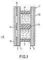
- There is shown in figure 1 a
display panel 1 having parallel front andback glass plates electrode structures front structure 7 is transparent and may be of tin oxide or other suitable conductive material. [A typical tin oxide film is of thickness -1 um with a sheet resistivity -1 to 1000 f2/0]. Theplates bistable medium 11, the medium thus being characterised by the property that, in regions where the two electrode structures overlap, it may be changed from one optical state (eg opaque) to another (eg transparent), when suitable voltages are applied to the electrodes of each of thestructures front plate 3 there is acover glass 13 and between these an opaque graduatedscale 15 and a central masking blank 17. - Though the medium 11 may be a solid layer of electroluminescent material, as in the case of an electroluminescent display panel; or, a rarefied gas, as in the case of an AC plasma discharge panel; for the purposes of this example it is a layer of liquid crystal material. The display panel thus adapted, is in the form of a liquid crystal cell where the liquid crystal material is enclosed in the space between the
glass plates peripheral spacer 19 of insulating material. For added rigidity there is also acentral support 21, also of insulating material. Theplates electrode bearing plates - In particular, for a cell using the cholesteric-to-nematic phase change effect the liquid crystal material is cholesteric and the plates may be treated by surfactant to give focal conic alignment. Examples of suitable cholesteric mixtures for such a cell are the mixtures:-
- E8* (nematic) with approx 6 wt % CB 15* (cholesteric), or
- E18* (nematic) with approx 6 wt % CB 15* (cholesteric),
- Preferably these cholesteric materials include in addition a small amount of pleochroic dye. For example an anthraquinone dye such as D16* (see also UK Patent Application No. 42,810/77). * The materials E8, E18, CB15, and dye D16 are listed in the trade catalogues of BDH Ltd., Poole, Dorset, England.


- Whilst the liquid crystal cell, so far as described above, may be viewed with back illumination, it is here shown as a reflective device and has, adjacent the
back plate 5, areflector 23 which may be a specular or diffusely reflecting metal film (eg silver, aluminium), or, a diffusely reflecting white paint, or card. - The
electrode bearing plates spacer 19 to facilitate external connection to theelectrode structures - Particular configurations of the
electrode structures - The back electrode structure comprises ten segment portions S0, S1,... S9 arranged to form a circular array. Each one of the segments SO,... S9 has
component parts parts 9a are each in the form of a shaped segment, and thepart 9b is in the form of a peripheral background electrode adjacent and nearly surrounding theparts 9a. Theelectrode 9b, as shown, has a number of thin outwardly extendinglimbs 9b', which limbs extend between theparts 9a and are isolated from them by narrow spacing. Thelimbs 9b' are integrally connected, to form thesingle background electrode 9b, by acentral ring conductor 9b". Consequently, the whole of the display area provided by segments S0,... S9 is almost completely spanned by the material of theelectrodes sectors 9a of the segments SO, ... S9 are connected to pad terminals T0, ... T9 respectively; and thebackground electrode 9b is connected to a single terminal TX by connecting strips 25 (shown schematically). Since thelimbs 9b' of thebackground electrode 9b are connected centrally, the connections to the terminal may be made without bridging the connecting strips 25 on theback plate 5. It is noted that in the absence of central connection, 9b", the number of terminals TX would be unduly multiplied to avoid bridging. - To afford display of two index characters made distinct by different shape, the segment electrodes are shaped to provide long hand and short hand index regions. Each
segment electrode 9a, as shown, has extendedlimbs 9a', 9a" andforeshortened limbs 9a". Theextended limb 9a' of eachsector 9a is lengthened to facilitate connection to the terminals TO,... T9. When registered with the meander electrodes of thefront electrode structure 3, the shapedelectrode 9a of the first segment SO provides five long hand index regions R01, R03, ... R09 and four short hand index regions R02, R04, R08 as determined by electrode overlap. (These regions are delineated in figure 3, to show this overlap, by broken outline). Similarly in the adjacent segments, Si (i = 1 to 9), long hand index regions Ri1, Ri3, ... Ri9, and short hand index regions Ri2, Ri4, ... R/8 are determined by corresponding electrode overlap. - The
front electrode structure 7 comprises a set of electrodes including a first sub-set of five strip electrodes E1, E3, ... E9. These electrodes are shaped and arranged in a modified meander configuration and are registered A' upon A' to delineate the long hand index regions, eg the strip electrode E1 overlaps the segments S0, S1, ... S9 delineating the index regions R01, R19, ... R99. Similarly electrode E9 delineates the index regions R09, R11, R91. Alternating with electrodes E1, E3, ... E9 is a second sub-set of five strips electrodes E0, E2, ... E8. These electrodes overlap the short hand index regions and also thelimbs 9b' of theperipheral electrode 9b. Thus the strip electrode E2 overlaps the segments S0, S1, ... S9 and delineates the index regions R02, R18, ... R98. The strip electrode E8 similarly delineates the index regions R08, R12, ... R92. The electrode EO however overlaps thelimbs 9b'. - Circuitry, suitable for operating the
display panel 1 having the electrode configurations described, is shown in figures 5a, 5b. - There is shown in figure 5a a
signal generator 31 and asignal selector 33. Thesignal generator 31 comprises a 12-bit serial-in/parallelout shift register 35 cooperative withlogic feedback components shift register 35 has twelve output ports P0, ... P11 which feed twelve signal lines L0, ... L11. In operation the voltage signals on these lines change from logic'1' to logic '0' ie Hi and Lo voltage levels, respectively, (according to the logic states of the corresponding register bits), as theshift register 35 is driven by the clocking pulses of an oscillator clock CP. The frequency of these is ideally ≥ 400Hz to avoid flicker. The voltage signals are differently phased, as ensured by the shift register. Consequently, the first and fourth signal lines LO and L3 control the input port I of theregister 35 throughlogic feedback components OR gate 39. This ensures that on initiation the input I is held Hi and changes the logic state of the first bit ofregister 35, corresponding to output port P0, line L0, from the logic '0' to the logic '1' state on the first clock edge. After a short initiation interval corresponding to the input of a small number of clocking pulses, the feedback throughcomponents register 35 is clocked, this feedback ensures that the first four bits are changed from one set of logic states to another in a recurrent but pseudo-random sequence as shown in table 1 below:
- The pseudo random sequence output signals from ports PO to P11, provided after the initiation interval, are shown in table 2 below:-

- The difference between any two signals is nett Ac and has an RMS value of (8/15)1/2. V, where V is the voltage difference between the Lo logic '0' and Hi logic '1' levels. It is preferable that all finite RMS voltage differences developed across the panel are greater than 1.1 times the saturation voltage characteristic of the
liquid crystal material 11. - If the logic voltage levels provide RMS differences compatible with the drive requirements of the display panel, the signals on signal lines LO, ... , L10 lay be applied directly to the input terminals TO to T9 and TX of the back
plate electrode structure 9. However, if the RMS differences were not compatible, the signals on lines L0, L10 could be applied to terminals TO to T9 and TX via matching amplifiers. - The
signal selector 33 comprises two 10:1multplexers multiplexers 51, ... 55 and, a second set of four 2:1multiplexers 61, ... , 64. Each of the 10:1multiplexers 43A, 438 has tensignal inputs 10, ... , 19 one connected to each of the signal lines Lo, ... , L9. Each 10:1multiplexer inputs 10 to 19 are connected respectively to the output port 0. The 10:1multiplexer 43A and the first set of 2:1multiplexers 51 to 55 are dedicated to the display of one of the two index characters (ie the long hand) and similarly the 10:1 multiplexers 438 and the second set of 2:1multiplexers 61 to 64 are dedicated to the display of the other distinctive index character (ie the short hand). - Each of the 10:1
multiplexers - Each 2:1
multiplexer 51 to 55, 61 to 64 has a first and second signal input port 10',11' and an output port 0'. The 2:1multiplexers 51 to 55 have each a secondary control input e to i, and the 2:1multiplexers 61 to 64, secondary control inputs e to h. If the secondary control input is at logic "1" then the output port O' is connected to 11, and if at logic "O" then the output port is connected to 10'. The output ports 0' of the 2:1multiplexers 51 to 55 are connected either directly, or, if necessary, via matching amplifiers, to the front- plate electrodes E1, E3, ... , E9, whilst those of the 2:1multiplexers 61 to 64 are connected in like manner to electrodes E2, E4, E6 and E8, respectively. The first signal input ports 11' of 2:1multiplexers 51 to 55 are connected in parallel to the output port 0 of the 10:1multiplexer 43A, and in like manner the first signal input ports 11' of 2:1multiplexers 61 to 64 are connected to the output port 0 of the 10:1multiplexer 43B. - The first set of 2:1
multiplexers 51 to 55 are responsive to secondary control signals which may be supplied to their control inputs e to i. Collectively these 2:1 multiplexers have the function of channeling the selective signal from the output port O of the 10:1multiplexer 43A onto a selected one of the front plate electrodes E1, E3 to E9 according to the secondary control signal coding. In this way, therefore, an applied signal may be selected and channeled to a selected one of the meander electrodes E1, E3 to E9 so that across the region of the medium 11 of thedisplay panel 1 delineated by the intersection of the selected meander electrode and the segment electrode to which this selected signal is also applied, a zero RMS difference voltage is developed since like signals are applied to the selected meander electrode and the appropriate segment electrode. The medium 11 in this delineated region is thus held in the OFF state for the duration of these like signals. - The second set of 2:1
multiplexers 61 to 64 function in similar manner to channel the selected signal from the output port 0 of the 10:1multiplexer 43B onto a selected one of the second subset of front plate electrodes E2, E4, E6 and E8 to produce the OFF state in another region of the medium 11. - The second signal inputs 10' of the 2:1
multiplexers 51 to 55, and 61 to 64 are connected in parallel to signal line L11. These multiplexers ensure that the signal on this line is channeled directly, or where appropriate through amplifiers, to the remaining-and-non-selected meander electrodes E1 to E9. The meander electrode EO is connected directly, or through a matching amplifier, to line L11. The voltage signal online L1 1 is different from all signals applied to the terminals TO to T9 and TX and consequently across all other regions of the medium 11 delineated by the overlap of the front and back-plate electrode structures - - . There are shown in figure 5b the component parts of a control data source for providing the primary and secondary control data signals to operate the
signal selector 33. This source comprises: aninput transducer 80; anA-D converter 81 including timing circuits and sampling means (not shown) where necessary; two pairs of 1:5 demultimplexers: pair 83A and 83B, and pair 85A and 85B each with an associated invertingamplifier gates 91 to 99, two of these 92, 98 being 3-input OR gates. - The
input transducer 80 provides an analogue signal as an electrical measure of some scalar function (eg pressure) and this signal is coded byA-D converter 81 to produce logic signals in a binary-coded- decimal (BCD) form at three sets of four outputs a to d corresponding the binary coded units (1's), tens (10's) and hundreds (100's) of the digitised analogue values, a being the most significant, and d the least significant bit outputs. - The outputs a to d corresponding to the tens and hundreds provide the primary control data signals for the 10:1
multiplexers - The first pair of 1:5
multiplexers convertor 81. The least significant bit output d of the next adjacent section, the tens section, provides a logic signal '0' or '1' at the input port of 1:5demultiplexer 83A to which it is connected directly, and an inverted logic signal '1' or '0' at the input port of 1:5demultiplexer 83B to which it is connected via invertingamplifier 84. This pair of 1:5demultiplexers multiplexers 51 to 55. Since one or other of the input logic signals is a logic '1', a logic '1' signal is fed onto one of the five output channels a0 to a4 of thedemultiplexer 83B or one of the five output channels a5 to a9 of thedemultiplexer 83A, all of the other outputs being simultaneously at logic '0'. All the output channels are connected to the inputs of the ORgates multiplexers 51 to 55. The output channels-ao to a9 are connected to the OR gates, 91, 93, ... , 99 in the order:- a4, a5 to 99; a3, a6 to 97; a2, a7 to 95; a1, a8 to 93; and a0, a9 to 91. The pairing of the multiplexers, and the use of the OR gates, compensates for the reversing characteristic of the meander structure, enabling the index positions R01, R03 to R99 to be selected consecutively with increasing values of the analogue signal. - The 1:5
multiplexers 85A, 85B are both controlled by the three most significant bit outputs of the tens section of theconvertor 81. The least significant bit output d of the hundreds section provides logic signals '1' or '0' to demultiplexers 85A, 85B in manner similar to that above and a logic '1' is fed onto one of the control inputs e to h of the second set ofmultiplexers 61 to 64 after being channelled onto one of the ten output channels 60 to b9 of demultiplexers 85B, 85A and through one of the ORgates gates gates - The combination of this control data source with the
signal selector 33,signal generator 31 anddisplay panel 1 provides a meter display whereby values between 0 and 998 may be represented by a short-hand index character indicating the hundreds value, and the long-hand index character indicating the tens and units value of the measured scalar function. - The operation of this meter display may be illustrated by considering the response of the display to a slowly increasing scalar function, the BCD data running in unit increments from zero. Thus, initially, the three sets of four bit outputs a to d of the
convertor 81 are in the 0000 condition. In response to this, the outputs of invertingamplifiers demultiplexers 83B, 85B are held at logic level '1'. All other demultiplexer outputs a1 to a9, and b1 to b9 are set at logic level '0'. A logic level '1' is thus applied viagates multiplexers multiplexers multiplexers convertor 81. Thus in both cases, the voltage signal on the first line LO fromshift register 35, which is applied via terminal TO to segment S0, is also channeled to the frontplate electrodes E1, E2. Thus at the regions of overlap of these electrodes E1, E2 with segment S0, ie at the index regions R01, R02, the medium 11 is held in the OFF state, there being zero RMS voltage difference applied across thepanel 1 since the like signals are applied to these particular overlapping electrodes. Thus in the case of the cholesteric-nematic phase change liquid crystal cell with pleochroic dye, the liquid crystal material is maintained in the cholesteric phase (OFF state) and absorbs incident light. Since finite RMS voltage differences are applied across all other index regions R03 to R99, the medium 11 is held in the ON state and in the case of the liquid crystal cell above, the liquid crystal material is switched to, and maintained in, the nematic phase (ON state) where the dye absorption is greatly reduced, incident light being reflected from the reflector in these regions. A long-hand index character is displayed to indicate the 00 on thescale 15 with the short hand index character displayed in the immediately adjacent index position, both in optical contrast against the background of the display. - Upon the first increment of the BCD data, the units data changes from 0000 to 0001, the tens and hundreds data remaining unchanged. This change however produces no response since the first pair of
demultiplexers demultiplexers 83B from channel aO to channel a1 and in consequence, the signal on line LO is switched from electrode E1 to electrode E3 and the position of the displayed long-hand index character is changed from region R01 to R03 to indicate 02 on the graduatedscale 15. - As the BCD data is further incremented through units data states 0100, 0110, 1000 the position of the displayed long-hand index character changes progressively in a clockwise direction around the scale to indicate 04, 06, 08 on the graduated
scale 15 as the signal on line LO is switched by the first set of 2:1demultiplexers 51 to 55 to front-plate electrodes E5, E7, E9. On the next increment, the units data changes to 1001 without causing further change. On the next increment, however, the units data state is reset to 0000 and the tens data state changes from 0000 to 0001. Control, in consequence, shifts to demultiplexer 83A and a logic level '1' signal is switched to channel a5 and viaOR gate 99 to the secondary control input i ofdemultiplexer 55. The particular voltage signal selected bymultiplexer 43A is thus applied to back-plate electrode E9. The primary control data address of thismultiplexer 43A has been changed from 0000 to 0001 and, therefore, it is the signal on line L1, applied to terminal T1 and segment S1, that is selected. The long-hand index character thus changes to the position of region R11 delineated by the overlap of the back-plate electrode E9 and the front plate electrode segment S1. On subsequent increments, as the units data state changes from 0000 to 0010, 0100, 0110 and 1000, the signal on line L1 is channeled to electrodes E7, E5, E3, E1, ie the electrodes taken in reverse order, and the long-hand index character changes position from region R11 to regions R13, R15, R17, R19 to indicatevalues scale 15. - After two more BCD data increments, the units data state is reset to 0000 and the tens data state changes from 0001 to 0010. These changes have three effects. Firstly, to change control from
demultiplexer 83A back to 83B again so that a logic T level signal is applied to control the secondary control input e ofmultiplexer 51 to select back-plate electrode E1. Secondly, to change the signal selected bymultiplexer 43A, to the signal on line L2, so that the long-hand index character moves from the position of region R19 to the position of region R21 to indicate a value 20 on the graduatedscale 15. Thirdly, to change the state of demultiplexer 85B so that the signal selected bymultiplexer 43B ie the signal on line L0, is switched from front plate electrode E2 to front plate electrode E4. The position of the short-hand index character thus changes from the position of region R02 to the position of region R04. After a further twenty BCD data increments, the tens data state changes from 0010 to 0100 with a further movement of the short-hand index character to the position of region R06. Another twenty increments, and the shorthand moves to the position of region R08. But, after the next twenty increments, the position of the short-hand index character does not change since channels b3, b4 both control the same secondary control input h ofmultiplexer 64 through 3-input ORgate 98. The short hand index character thus "marks time" for yet a further twenty increments, until the hundreds data state changes from 0000 to 0001 and both the tens and units data states are reset to 0000. When this change takes place, however, the long-hand index character returns to the position of the region R01 having made a full revolution of the dial. The short-hand index character moves into the second segment S1 to the position of region R12. - The circuitry of figure 5a may be simplified quite readily to provide only tens and units meter indication, ie the analogue display may be simplified for display of a single index character. Since in this simplified form of the display, hundreds indication by the short-hand index character is not required, the 10:1
multiplexer 43B and its associated set of 2:1multiplexers 61 to 64 may be omitted. To maintain the short-hand index regions of the display in the ON state so to afford overall a contrasting background, the front-plate electrodes E2, E4, E6 and E8 with EO are connected in parallel to line L11 of the shift register and as shown in broken outline in figure 5a. - Alternative configurations of the front- and back-
plate electrode structures - The configuration of the back
plate electrode structure 9 is shown in outline in figure 6. The structure is divided into twelve segment electrodes SO to S11, and a common complementary electrode 9x. Each segment electrode is of complex shape, as shown in figure 7, and in combination with thefront plate structure 7 in Figure 8, defines, at these regions of overlap, five seconds (s), five minutes (m), and five hours (h), index character regions having marker, long-hand and, short hand shapes, respectively. For the even segments S0, S2, ... S10 the segment electrode is shaped to define these regions in the orders s m h s h m s m h s h m s m h; whilst for the odd segments S1, S3, ... S11, the segment electrode is shaped to define these regions in the reverse order s h m s m h s h m s m h s h m. It is noted that the seconds marker regions (s) are spaced evenly on anarcuate strip 9a whilst the minute and hour character regions (m) and (h), respectively, alternate about these seconds marker regions (s). This complex configuration allows access from the inside of the circle to the spaces X between inwardly extending portions of the segment electrode. The spaces X are filled in, but for a narrow isolating spacing from the inside perimeter of each segment electrode, with electrode material to form the commoncomplementary electrode 9X, the many portions of which are linked together by an inner circular ring. Each segment SO to S11 is connected to a corresponding terminal pad TO to T11. The commoncomplementary electrode 9X is connected to an auxiliary terminal pad TX. - As shown in figure 8, the front
plate electrode structure 7 comprises fifteen strip electrodes arranged in a modified meander configuration. These provide three subsets {E1, E4, E7, E10, E13}, {E2, E6, E8, E12, E14} and {E3, E5, E9, E11, E15} which, on assembly of thedisplay panel 1, are arranged in register to overlap the shaped segment electrodes SO to S11, to define the seconds, minutes, and hours index regions s, m, and h, respectively. - Circuitry for operating a
display panel 1 having the electrode configurations shown in figures 6, 7 and 8 and as above described, is shown in figures 9a to d. - There is shown in figure 9a a
signal generator 131 and asignal selector 133. Thesignal generator 131 comprises: a 14-bit serial in/parallelout shift register 135 having fourteen signal bit lines Lo to L13, one corresponding to each bit of the register; and, feed-back logic components, namely an exclusive ORgate 137, an ORgate 139 and a 4-input NORgate 141. Thelogic components register 135, as shown, and in a manner identical to that already described for thelogic components backplate electrode structure 9. The shift register is driven by clock-pulses derived indirectly from an oscillator clock at Z on figure 9b, the clock-pulses having a repetition frequency typically greater than 400 Hz to avoid flicker on the display. - The
signal selector 133 comprises, three 12:1multiplexers multiplexer multiplexer multiplexer multiplexers 151 to 155,161 to 165, and 171 to 175 has a secondary control input port, namely input ports e, to i, respectively. The first set of 2:1 multiplexers {151 to 151} are connected, either directly, or indirectly via matching amplifiers, to the first subset of front-plate electrodes {E1, E4, E7, E10, E13) so that the appropriate signal selected by 12:1multiplexer 143A may be channeled to one of these electrodes, under secondary control, for positioning the seconds index character. Similarly, the second and third set of 2:1 multiplexers {161 to 165} and {171 to 175} are connected to the second and third subsets of front plate electrodes, namely subsets {E2, E6, E8, E12, E14} and {E3, E5, E9, E11, E15} for positioning the minutes and hours index characters, respectively. - The clock pulses, the primary and the secondary control signals, required to operate the circuitry described above are provided by other circuitry which is now described with reference to figures 9b to d. This other circuitry comprises: an oscillator clock CP; a
scaling divider 201 for scaling down the frequency of the clock pulses provided by this clock CP by a factor N so as to provide, on an output line Z, clock pulses suitable for driving the shift register 135 (i.e. clock pulses having a frequency greater than or of the order of about 400 Hz); and a divider chain adapted to provide the primary and secondary control signals. This divider chain includes ascaling divider 203 responsive to the oscillator clock CP for dividing down the frequency of the clock pulses by a scale factor M to provide after division, a signal having a pulse repetition frequency of precisely 2 HS. Thisdivider 203 is followed by a ÷10counter 205 and thereafter by a first ÷12counter 207. This first ÷12counter 207 has four counter outputs a to d which provide the primary control signals formultiplexer 143A. Thiscounter 207 also provides, at its most significant bit output d, a first logic reference waveform of period one minute. During normal timing operation, this first logic reference is channeled through a first 2:1multiplexer 209 to the input port of a ÷5counter 211, and this latter is followed by a second +12counter 213. The second ÷12counter 213 has four counter outputs a to dwhich provide the primary control signals for multiplexer 143B. Thiscounter 213 also provides at output d, a second logic reference of period one hour. This second reference is channeled through a second 2:1multiplexer 215 to a third ÷12counter 217. The third ÷12counter 217 has four counter outputs a to dwhich provide the primary control signals formultiplexer 143C. - Secondary control signals for the 2:1
multiplexers 151 to 135, 161 to 165, and 171 to 175 are provided at output ports e to i of threedecoders decoders 219 is connected to receive signal codes from the three most significant bit output ports b, c, and d of the -10counter 205, and the least significant bit output port a of the first 12counter 207. Similarly, the second of thesedecoders 221 is connected to receive signal codes from the three most significant bit outputs b, c and d of the +5counter 211, and the least significant bit output ports b, c and d of the -5counter 211, and the least significant bit output port a of the second -12counter 213. However, the third of thesedecoders 223 is connected to the four output ports a to d of a second -10counter 225. A ÷12divider 227 is connected to the output port of the first 211multiplexer 209 to receive, under normal conditions, the first logic reference and to reduce its frequency by twelve. The output port of thisdivider 227 is connected to one of the two input ports of a third 2:1multiplexer 229. Under normal timing conditions the divided signal passed on to this input is channeled to the clock input of the -10counter 225. - The first 2:1
multiplexer 209 has a second input connected to the least significant bit output port a of the -10counter 205.Multiplexer 209 has a control input kwhich normally is connected to the logic '0' level supply voltage Vss supply by means of a biased charge over push button switch SM. This combination allows manual over-ride of the normal timing conditions. When the switch SM is operated the control input k ofmultiplexer 209 is connected directly to the VDD voltage supply and held at logic '1' level. In response the output signal from 209 is changed from one of one minute period (ie that from output port d of ÷12 counter 207) to one of one second period (i.e. that from output port a of ÷10 counter 205). In consequence of this change the minute hand index character may be advanced more rapidly, changing from one minute position to the next once every second, until it reaches a desired synchronising position. Since the ÷12divider 227 responds immediately to this change, and the third ÷12counter 217 responds indirectly throughcounters - The second and
third multiplexers 214, 229 have controlling input ports k each connected to the source of the logic '0' supply voltage Vss through a biased changeover push button switch CH. Bothmultiplexers counter 205. Thus when the switch SH is closed a logic'1' level voltage is applied to the control port k of bothmultiplexers
characterised in that:
Claims (12)
characterised in that:-
the panel address means comprises
Applications Claiming Priority (2)
| Application Number | Priority Date | Filing Date | Title |
|---|---|---|---|
| GB7902941 | 1979-01-26 | ||
| GB7902941 | 1979-01-26 |
Publications (3)
| Publication Number | Publication Date |
|---|---|
| EP0014100A2 EP0014100A2 (en) | 1980-08-06 |
| EP0014100A3 EP0014100A3 (en) | 1981-11-04 |
| EP0014100B1 true EP0014100B1 (en) | 1985-06-05 |
Family
ID=10502775
Family Applications (1)
| Application Number | Title | Priority Date | Filing Date |
|---|---|---|---|
| EP80300236A Expired EP0014100B1 (en) | 1979-01-26 | 1980-01-24 | Analogue display |
Country Status (7)
| Country | Link |
|---|---|
| US (1) | US4326279A (en) |
| EP (1) | EP0014100B1 (en) |
| JP (1) | JPS55108692A (en) |
| AU (1) | AU531051B2 (en) |
| CA (1) | CA1138211A (en) |
| DE (1) | DE3070727D1 (en) |
| GB (1) | GB2044975B (en) |
Families Citing this family (10)
| Publication number | Priority date | Publication date | Assignee | Title |
|---|---|---|---|---|
| DE3034454A1 (en) * | 1980-09-12 | 1982-04-15 | Eurosil GmbH, 8000 München | QUASI ANALOG DISPLAY DEVICE |
| CH642227B (en) * | 1981-10-28 | Asulab Sa | WATCH WITH ANALOGUE DISPLAY DEVICE WHOSE DIAL IS SHAPED BY A LIQUID CRYSTAL DISPLAY CELL. | |
| EP0086551A3 (en) * | 1982-02-01 | 1987-05-13 | National Research Development Corporation | Character display panels and panel devices |
| EP0109160A3 (en) * | 1982-10-14 | 1986-04-09 | The Secretary of State for Defence in Her Britannic Majesty's Government of the United Kingdom of Great Britain and | Electronic displays |
| US4547773A (en) * | 1983-01-19 | 1985-10-15 | National Research Development Corporation | Character display panels and panel devices |
| GB8408216D0 (en) * | 1984-03-30 | 1984-05-10 | Secr Defence | Flat-panel display |
| US6327010B1 (en) | 1992-02-03 | 2001-12-04 | Merck Patent Gesellschaft Mit Beschrankter Haftung | Electrooptical system |
| US5477358A (en) * | 1993-06-21 | 1995-12-19 | Case Western Reserve University | Chiral nematic liquid crystal display with homeotropic alignment and negative dielectric anisotropy |
| US6556179B2 (en) * | 1997-02-17 | 2003-04-29 | Nikon Corporation | Display device and camera having the display device |
| AU2001253747A1 (en) * | 2000-04-21 | 2001-11-07 | Diikon Technologies Llc | Monitoring device with automatic visual time expiration indicator |
Family Cites Families (18)
| Publication number | Priority date | Publication date | Assignee | Title |
|---|---|---|---|---|
| JPS4984474A (en) * | 1972-12-18 | 1974-08-14 | ||
| US3982239A (en) * | 1973-02-07 | 1976-09-21 | North Hills Electronics, Inc. | Saturation drive arrangements for optically bistable displays |
| US4044345A (en) * | 1973-03-27 | 1977-08-23 | Mitsubishi Denki Kabushiki Kaisha | Method for addressing X-Y matrix display cells |
| GB1478592A (en) | 1974-03-01 | 1977-07-06 | Secr Defence | Liquid crystal devices |
| GB1472247A (en) | 1974-02-21 | 1977-05-04 | Secr Defence | Liquid crystal devices |
| US3895373A (en) * | 1974-06-07 | 1975-07-15 | Ibm | Method and apparatus for selectively exciting a matrix of voltage responsive devices |
| US4119367A (en) * | 1975-03-06 | 1978-10-10 | Edward Peter Raynes | Liquid crystal displays |
| GB1559074A (en) * | 1975-11-05 | 1980-01-16 | Nat Res Dev | Electonic analogues waveform displays |
| DE2551542A1 (en) * | 1975-11-17 | 1977-05-26 | Joachim Reich | ELECTRONIC CLOCK |
| US4077032A (en) * | 1976-01-07 | 1978-02-28 | Volkman S Alan | Electronic display apparatus |
| JPS52103993A (en) * | 1976-02-11 | 1977-08-31 | Rank Organisation Ltd | Liquid crystal display unit |
| GB1526266A (en) * | 1976-09-22 | 1978-09-27 | Secr Defence | Matrix addressing of liquid crystal displays |
| US4186395A (en) * | 1977-03-01 | 1980-01-29 | Kabushiki Kaisha Seikosha | Method of driving a liquid crystal display apparatus |
| US4250503A (en) * | 1977-07-26 | 1981-02-10 | National Research Development Corporation | Apparatus for displaying waveforms on a matrix display |
| US4227193A (en) * | 1977-07-26 | 1980-10-07 | National Research Development Corporation | Method and apparatus for matrix addressing opto-electric displays |
| CH616231A5 (en) * | 1977-07-29 | 1980-03-14 | Bbc Brown Boveri & Cie | |
| US4212159A (en) * | 1978-02-13 | 1980-07-15 | Texas Instruments Incorporated | Electronic timepiece |
| US4212011A (en) * | 1978-08-30 | 1980-07-08 | General Electric Company | Multimode liquid crystal display |
-
1980
- 1980-01-21 GB GB8001993A patent/GB2044975B/en not_active Expired
- 1980-01-24 EP EP80300236A patent/EP0014100B1/en not_active Expired
- 1980-01-24 DE DE8080300236T patent/DE3070727D1/en not_active Expired
- 1980-01-25 AU AU54954/80A patent/AU531051B2/en not_active Ceased
- 1980-01-25 US US06/115,535 patent/US4326279A/en not_active Expired - Lifetime
- 1980-01-25 JP JP822980A patent/JPS55108692A/en active Pending
- 1980-01-25 CA CA000344398A patent/CA1138211A/en not_active Expired
Also Published As
| Publication number | Publication date |
|---|---|
| AU5495480A (en) | 1980-07-31 |
| AU531051B2 (en) | 1983-08-11 |
| GB2044975A (en) | 1980-10-22 |
| CA1138211A (en) | 1982-12-28 |
| JPS55108692A (en) | 1980-08-21 |
| EP0014100A3 (en) | 1981-11-04 |
| GB2044975B (en) | 1982-12-08 |
| DE3070727D1 (en) | 1985-07-11 |
| US4326279A (en) | 1982-04-20 |
| EP0014100A2 (en) | 1980-08-06 |
Similar Documents
| Publication | Publication Date | Title |
|---|---|---|
| US3540209A (en) | Horological time display | |
| EP0014100B1 (en) | Analogue display | |
| US4346378A (en) | Double trace electro optic display | |
| US5214624A (en) | Display device having a scale | |
| US4403832A (en) | Liquid crystal display device | |
| US4449125A (en) | Matrix display device | |
| US4250503A (en) | Apparatus for displaying waveforms on a matrix display | |
| US4626840A (en) | Electronic display suitable for polar coordinate representations | |
| US4342030A (en) | Analogue displays for electronic timepieces or meters | |
| KR100427161B1 (en) | Watch with liquid crystal display panel | |
| US3878537A (en) | Multiplexed liquid-crystal display device | |
| US4258364A (en) | Display device having adjoining display elements, and a method of producing the display device | |
| US4227193A (en) | Method and apparatus for matrix addressing opto-electric displays | |
| US3898642A (en) | Coplanar analog display devices of the variable length bar type | |
| US3789388A (en) | Apparatus for providing a pulsed liquid crystal display | |
| US4119367A (en) | Liquid crystal displays | |
| US4382659A (en) | Liquid crystal display device | |
| US4346964A (en) | Electrochromic display device | |
| CA1217586A (en) | Matrix display control process | |
| US4147416A (en) | Electrochromic display device | |
| US4367959A (en) | Pseudo-analog display device | |
| US4099839A (en) | Faster addressing of electrochromic displays | |
| USRE29727E (en) | Digital display device | |
| GB1523162A (en) | Liquid crystal displays | |
| CA1042219A (en) | Solid-state display for time-piece |
Legal Events
| Date | Code | Title | Description |
|---|---|---|---|
| PUAI | Public reference made under article 153(3) epc to a published international application that has entered the european phase |
Free format text: ORIGINAL CODE: 0009012 |
|
| AK | Designated contracting states |
Designated state(s): CH DE FR IT NL |
|
| 17P | Request for examination filed |
Effective date: 19810116 |
|
| R17P | Request for examination filed (corrected) |
Effective date: 19810116 |
|
| PUAL | Search report despatched |
Free format text: ORIGINAL CODE: 0009013 |
|
| AK | Designated contracting states |
Designated state(s): CH DE FR IT NL |
|
| ITF | It: translation for a ep patent filed |
Owner name: BARZANO' E ZANARDO ROMA S.P.A. |
|
| GRAA | (expected) grant |
Free format text: ORIGINAL CODE: 0009210 |
|
| AK | Designated contracting states |
Designated state(s): CH DE FR IT NL |
|
| REF | Corresponds to: |
Ref document number: 3070727 Country of ref document: DE Date of ref document: 19850711 |
|
| ET | Fr: translation filed | ||
| PLBE | No opposition filed within time limit |
Free format text: ORIGINAL CODE: 0009261 |
|
| STAA | Information on the status of an ep patent application or granted ep patent |
Free format text: STATUS: NO OPPOSITION FILED WITHIN TIME LIMIT |
|
| 26N | No opposition filed | ||
| PGFP | Annual fee paid to national office [announced via postgrant information from national office to epo] |
Ref country code: NL Payment date: 19870131 Year of fee payment: 8 |
|
| PG25 | Lapsed in a contracting state [announced via postgrant information from national office to epo] |
Ref country code: CH Effective date: 19880131 |
|
| PG25 | Lapsed in a contracting state [announced via postgrant information from national office to epo] |
Ref country code: NL Effective date: 19880801 |
|
| NLV4 | Nl: lapsed or anulled due to non-payment of the annual fee | ||
| PG25 | Lapsed in a contracting state [announced via postgrant information from national office to epo] |
Ref country code: FR Free format text: LAPSE BECAUSE OF NON-PAYMENT OF DUE FEES Effective date: 19880930 |
|
| REG | Reference to a national code |
Ref country code: CH Ref legal event code: PL |
|
| PG25 | Lapsed in a contracting state [announced via postgrant information from national office to epo] |
Ref country code: DE Effective date: 19881001 |
|
| REG | Reference to a national code |
Ref country code: FR Ref legal event code: ST |