EP0007276A1 - Einrichtung für die Demodulation von frequenzumgetasteten Signalen - Google Patents
Einrichtung für die Demodulation von frequenzumgetasteten Signalen Download PDFInfo
- Publication number
- EP0007276A1 EP0007276A1 EP79400481A EP79400481A EP0007276A1 EP 0007276 A1 EP0007276 A1 EP 0007276A1 EP 79400481 A EP79400481 A EP 79400481A EP 79400481 A EP79400481 A EP 79400481A EP 0007276 A1 EP0007276 A1 EP 0007276A1
- Authority
- EP
- European Patent Office
- Prior art keywords
- input
- electrodes
- output
- signals
- signal
- Prior art date
- Legal status (The legal status is an assumption and is not a legal conclusion. Google has not performed a legal analysis and makes no representation as to the accuracy of the status listed.)
- Granted
Links
Images

Classifications
-
- H—ELECTRICITY
- H03—ELECTRONIC CIRCUITRY
- H03H—IMPEDANCE NETWORKS, e.g. RESONANT CIRCUITS; RESONATORS
- H03H9/00—Networks comprising electromechanical or electro-acoustic devices; Electromechanical resonators
- H03H9/46—Filters
- H03H9/64—Filters using surface acoustic waves
- H03H9/6403—Programmable filters
-
- H—ELECTRICITY
- H03—ELECTRONIC CIRCUITRY
- H03H—IMPEDANCE NETWORKS, e.g. RESONANT CIRCUITS; RESONATORS
- H03H9/00—Networks comprising electromechanical or electro-acoustic devices; Electromechanical resonators
- H03H9/02—Details
- H03H9/02535—Details of surface acoustic wave devices
- H03H9/0296—Surface acoustic wave [SAW] devices having both acoustic and non-acoustic properties
-
- H—ELECTRICITY
- H04—ELECTRIC COMMUNICATION TECHNIQUE
- H04L—TRANSMISSION OF DIGITAL INFORMATION, e.g. TELEGRAPHIC COMMUNICATION
- H04L27/00—Modulated-carrier systems
- H04L27/10—Frequency-modulated carrier systems, i.e. using frequency-shift keying
- H04L27/14—Demodulator circuits; Receiver circuits
- H04L27/144—Demodulator circuits; Receiver circuits with demodulation using spectral properties of the received signal, e.g. by using frequency selective- or frequency sensitive elements
- H04L27/148—Demodulator circuits; Receiver circuits with demodulation using spectral properties of the received signal, e.g. by using frequency selective- or frequency sensitive elements using filters, including PLL-type filters
Definitions
- the present invention relates to devices for demodulating signals modulated by frequency displacement and composed of sequences deducing from each other by circular permutations, and in particular signals modulated by frequency displacement at minimum spectrum.
- a modulation by frequency spectrum shifting is a coded dual frequency modulation, characterized by a modulated signal having a constant amplitude, a continuous phase variation, and a minimal spectral bulk. According to certain publications (IEEE Transactions on Communications, April 1977 page 433) this modulation is considered, during the duration of each sequence, either as a modulation by displacement of frequency of a signal of frequency F c (modulation FSK or Frequency Shift Keying in Anglo-Saxon literature), the resulting modulated signal having two frequencies F + and F c - (Fb being the frequency of the transmitted bits), or as a special case of modulation with quaternary phase displacement (QPSK or Quaterary Phase Shift Keying modulation in the Anglo-Saxon literature).
- the two carriers are respectively multiplied analogically by the two modulating signals; it should be noted that this modulation causes, for each modulated carrier, a phase modulation o or ⁇ at each cancellation of the amplitude of the modulating signal.
- phase-controlled demodulators as described in IEEE Transactions on Communications, October 1973 page 1529
- These demodulators are suitable for demodulation of a continuously modulated signal but not for demodulation of a sequence modulated signal.
- the object of the present invention is to remedy the drawbacks of these demodulators.
- a device for demodulating signals modulated by frequency displacement these signals being made up of sequences of n oscillation trains (n integer greater than 1), each train being of given frequency and given duration ⁇ and resulting from the addition of two wave trains of frequency F in phase quadrature and respectively amplitude modulated by two modulation signals, each of the modulation signals being constituted by the juxtaposition of signals of given form and of given duration 2 ⁇ , and can be positive or negative, the given frequencies of each sequence being representative of a binary code with circular permutations, is characterized in that its input is coupled to its output by two filtering channels adapted to one of the sequences of n oscillation trains, in that each filtering channel has an input channel and an output channel common to the two filtering channels, and in that one of the input channels includes a delay device causing an increase in n ⁇ of the transit time by compared to transit time in the other route of entry.
- This sum signal c is a modulated signal "by frequency shift with minimum spectrum" having a continuous phase variation and a constant amplitude.
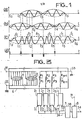
- phase shift at the origin between the carrier signal and the modulating signal is (particular case ie Figure 1), but it should be noted that this phase shift can take any value.
- the synthesis of a signal such as c can also be carried out with a filter having as impulse response the train of oscillations of frequency F c of the signal took between the instants t 1 and t 3 , and receiving on its input the signal d, of figure 1, made up of brief pulses of period ⁇ .
- a short negative pulse corresponds to a value of ⁇ i equal to - 1.
- the signal c represents a dual-frequency modulated signal whose two frequency values F 1 and F 2 can be used to translate a binary code with circular permutations.
- the binary coding with circular permutations of a first item of information generally results in a first sequence in which the bits are ordered in a predetermined manner, this sequence, called “basic sequence” in the following, being separated from the following by an absence of signal of a given duration.
- sequences comprising the following information, separated from one another by an absence of signal, are obtained by circular permutations of the initial sequence.
- This sequence modulation is a special case of "M-ary modulation", M being the number of circular permutations used.
- Each sequence of M bits corresponds to elementary information to be transmitted (for example a letter of the alphabet); so with a "basic sequence" such that the M sequences, deduced from each other by circular permutation, are not identical, it is possible to transmit M different elementary information.
- the purpose of demodulating such signals modulated by sequences of permutations by frequency displacement is to restore a pulse whose position in time, within a duration interval M. ⁇ is a function of the information received.
- a filter adapted to this sequence is understood by filter adapted to a train of oscillations of frequency F c or to a sequence as defined, a filter whose impulse response is the inverse over time of the train or of the sequence without taking account of the phase at the origin of the carrier frequency.
- a filter adapted to a signal of finite duration is the one whose impulse response is this same signal inverted over time.
- a filter 2 receiving the known code sequence of n bits on its input 20, supplies by its output 21, n delay lines L 1 to L n arranged in series and each imposing a delay equal to ⁇ .
- the output 21 of the filter 2 as well as the output of each delay line L 1 to L n are respectively connected to the n + 1 inputs of a summing device 3 whose output 22 constitutes the output of the matched filter. It should be noted that each input of the summing device 3 reverses or not the signal which is applied to it so as to allow the filter adapted to the known code sequence to be produced.
- the filter 2 presents an impulse response having the form of the train of oscillations of frequency F c , called "basic signal" in what follows, of the signal a of figure 1 taken between the instants t 1 and t 3 .
- the filter 2 is a filter adapted to this basic signal. It should be noted that it is desirable that the filters 2 of the demodulator and the emission filter must be produced simultaneously by the same masks (in monolithic integration), so that an accidental asymmetry of the emission filter is reproduced on the filter 2.
- Filter 2 receiving the sequence to be identified, provides a signal which is reproduced at the output of each delay line L 1 to L n with respective delays of value ⁇ to n ⁇ .
- All these output signals are summed algebraically by the summing device 3.
- This algebraic summing is carried out according to a code inverted in time of the emission code (signals e 1 and ⁇ 2 ) of the sequence transmitted (for example a reverse code in time to that of signal d in FIG. 1 if the sequence received is that of this signal).
- This demodulator therefore constitutes a filter adapted to this sequence to be identified.
- the principle of the demodulator according to the invention consists in adding to a filter suitable for a sequence known as "tuning", normally the "basic sequence", a device for repeating at one point or another of this filter making it possible to obtain from the demodulator, for a sequence received, the same response as if it had received it twice in a row.
- a surface acoustic wave filter comprising two input transducers coupled to the same output transducer, and each of which forms with the output transducer a filter such as filter 2 in FIG. 2, the difference in the path of the acoustic wave between the output of the two input transducers constituting the repeating device.
- a piezoelectric quartz substrate 6 comprises a first set of parallel metal electrodes, of different lengths and supplied in parallel by the signal received on the input 31.
- This substrate 6 also includes a second set of metal electrodes , parallel to each other and parallel to the electrodes of the first set, having different lengths, and having one end connected to the input 32 by a common connection, the input 32 itself connected to ground.
- These two sets of electrodes are interlaced and their interpenetration zone is symbolized by the outline 4 in dotted lines (corresponding to the shape of the impulse response of the filter).
- the substrate 6 comprises a fifth set of metal electrodes e 1 to e n + 1 , mutually parallel and parallel to the electrodes of the second set, having equal lengths having one end connected to the outlet 33 by a common connection, the outlet 33 being itself connected to ground.
- This substrate also includes a sixth set of metal electrodes e ' 1 to e' n + 1 , all of the same length, mutually parallel and parallel to the electrodes of the fifth set.
- These fifth and sixth sets of electrodes are interlaced, and have their electrodes e ' 1 to e' n + 1 respectively very close to the electrodes e 1 to e n + 1 but spaced apart from each other by a given distance 1, such that
- the notation e j + 1 - e j or e ' j + 1 - e' j means that we consider the distance between these electrodes.
- This given distance corresponds to.
- a propagation time equal to ⁇ (r being the aforementioned delay during the description of FIG.
- a first output of these switches is connected to an input (+) 35 of an algebraic summator 7, and a second output is connected to an input (-) 36 of this summator 7 having an output terminal 38 connected to the output 34 of the device, through a selection device 8 controlled by the signal received on the input 31.
- Logic signals T 1 to T n + 1 allow the switches I 1 to I n + 1 to be controlled to connect the electrodes e ' 1 to e' n + 1 respectively to input 35 if their logic state is in state "1" and to input 36 if their logical state is in state "O".
- the set of first and second sets of electrodes constitutes an input transducer which, by piezoelectric effect, converts the electrical signals received on the input 31 into an acoustic wave with a surface identical in shape to the electrical response of this transducer.
- the set of third and fourth sets of electrodes constitutes an output transducer which receives this wave and transforms it, by reverse piezoelectric effect, into an electrical signal (Proceeding of the IEEE, May 1976, Vol. 64, n ° 5, pages 581 to 595) identical in shape to that of the surface acoustic wave.
- all of the first and second sets of electrodes as well as the third and fourth sets of electrodes each constitute a filter having for impulse response a train of oscillations of frequency F c , the envelope of which is given by the periphery 4 of FIG. 3 (Proceeding of the IEEE, May 1976, vol. 64, n ° 5, pages 639 to 651).
- These assemblies therefore respectively constitute two filters such as filter 2 in FIG. 2, and the distance between the inputs makes it possible to repeat the sequence received.
- the set of third and fourth sets of electrodes is identical to a delay line comprising n elementary delays of value ⁇ .
- This delay line is therefore identical to the n delay lines in FIG. 2.
- the switches I 1 to I n + 1 make it possible to code this part of the demodulator, according to the inverse in time of the code of the "basic sequence", which will be called “chord code” in the following (this coding was carried out by the inputs of the summing device 3 of FIG. 2 for a fixed and known code).
- the coding of the demodulator (in “agreement code”) is carried out by the logic state of the signals T 1 to T n + 1 .
- this sequence is transferred from the input transducer having the interpenetration periphery 5 on the n +1 last pairs of electrodes e 1 , e ' 1 to e n + 1 , e' n + 1 of the output transducer, with a delay ⁇ ( ⁇ being the propagation time, in the substrate 6, between the transducers entry and exit).
- ⁇ being the propagation time, in the substrate 6, between the transducers entry and exit.
- T n ⁇ .
- the sequence present on the electrodes of the output transducer, and due to the sum of the partial information coming from the two input transducers, will coincide with the tuning sequence; at this instant the aforementioned maximum amplitude will appear. Then the information continues to propagate from one pair of electrodes to the next. It should be noted that the duration of propagation of the information on these pairs of electrodes, during which the output of the algebraic summator 7 is capable of delivering a signal, is 3n ⁇ .
- this maximum amplitude will generally be accompanied by two maxima of less or equal amplitude, these maxima being due to the fact that the information contained on the electrodes of the output transducer partially coincides with the "sequence of agreement". These two maxima will be located, temporally, on either side of the maximum amplitude. Hence the need for a device making it possible to select the maximum amplitude whose temporal position translates the useful information contained in the received sequence.
- This maximum amplitude can only be obtained between the instants t '+ n ⁇ + ⁇ and t' + 2n ⁇ + ⁇ if t 'is the reception start time (corresponding to the instant t of the signal c of the fi gure 1) of the sequence; it has been assumed in the foregoing that during transmission, the parts of the signal corresponding to those of signal c in the figure have been deleted (using a controlled switch arranged in series on the signal line) 1 between the instants t o and t 1 on the one hand and t 5 and t 6 on the other hand.
- the device making it possible to select and exploit the maximum amplitude is the selection device 8 of FIG. 3 which will be studied in detail in FIG. 5.
- chord sequence is not necessarily the "basic sequence", and that if one does not wish to have the possibility of modifying the "chord sequence” the switches I 1 to I n + 1 can be deleted and the algebraic summator 7 replaced by a simple adder.
- the demodulator is coded at the output transducer by placing the electrodes e i (1 ⁇ i ⁇ n + 1) upstream or downstream of the corresponding electrodes e ' i (relative to the direction of propagation of the surface acoustic wave) depending on whether you want a weighting by +1 or by -1.
- the repeating device is arranged upstream of a filter such as the filter 2 of FIG. 2.
- a first input 37 of an adder 9 is connected to an electrode t 1 and to the input 31 of the demodulation device.
- a second input of this summator 9 is connected to an electrode t 2 and its output is connected to an input transducer identical to that of FIG. 3 (perimeter of interpenetration 5).
- a pair of electrodes t 1 , t ' 1 (t' 1 being very close to the electrode t 1 and being connected to ground) is assa- ciée to a pair of electrodes t 2 , t ' 2 (t' 2 being very close to the electrode t 2 and being connected to ground).
- the electrodes e 1 to e n + 1 and e ' 1 to e' n + 1 , the switches I 1 to I n + 1 , the algebraic summator 7, the selection device 8 and the substrate 6 are identical to those of Figure 3 and connected together in the same way.
- this sequence is transferred to the first pair of electrodes of the output transducer with a delay 8 ( ⁇ being the propagation time in the substrate 6 between the input and output transducers).
- the input (+) of an analog comparator 11 is connected to terminal 38, through a detection circuit 10, the input (-) of this comparator 11 is connected to a threshold voltage V S , and the output of comparator 11 is connected to a first input of an AND gate, 12, having a second input connected to the output of a delay line 14.
- the output of AND gate, 12, is connected to a "clock" input a shift register 13 having five stages and having an output 34 constituting the output of the device.
- the outputs of the five stages of the counter 15 are respectively connected to the five respective inputs of the five stages of the shift register 13.
- the signal received by the detection circuit 10 is the output signal from the algebraic summator 7 ( Figures 3 and 4).
- This signal described previously during the study of FIG. 3, has a duration of 3n ⁇ (because the beginning and the end of the received sequence does not include a signal at frequency F) and includes the maximum useful pulse between the instants t '+ n ⁇ + ⁇ and t' + 2n ⁇ + 8 if t 'is the beginning of the sequence recapture.
- the detection circuit 10 and its associated low-pass filter (not shown) makes it possible to supply the input (+) of the comparator 11 with the positive envelope curve of the signal received on terminal 38.
- the comparator 11 provides at its output a logic "1" state when the amplitude of the signal received on its input (+) is greater than the threshold voltage V S and a logic "0" state otherwise.
- the output signal from this comparator 11 can therefore be in state “1” for the maximum useful amplitude, but also for the two amplitude maxima located in the first and last third of the duration 3n ⁇ of the received signal on terminal 38.
- the delay line 14 and the comp 15 associated with the AND gate, 12, allow the maximum useful amplitude to be selected.
- the output signal of the delay line (therefore on the second input of the AND gate, 12, and on the input 39 of the counter 15) is in state "1" logic at the instant t + n ⁇ + 9.
- This logic "1" state unlocks the counter 15 which counts from 0 to 31 for a duration n ⁇ (duration of the sequence received) at the rate of its clock of period T , and makes it possible to open the door AND, 12 and thus to select the maximum useful amplitude.
- the output signal of the AND gate, 12, is therefore in the logic "1" state during the counting period ⁇ corresponding to the position in time of the maximum useful amplitude.
- This logic state "1" then allows the shift register 13 to record the state of the counter. The content of this register is then read in serial form on its output 34.
- the invention is not limited to the embodiments described and shown, in particular the demodulation devices according to the invention can be produced according to the following variants.
- edges 4 and 5 of the interpenetration zones of the first and second sets of electrodes are identical to the signal, a (in FIG. 1) taken between the instants t 1 and t 3 , but with an envelope curve which is no longer consisting of a half-cycle of sinusoid but of a cycle of a quasi-sinusoidal signal with continuous derivatives until an unspecified order, if this is the case for the emission filter.
- the substrate 6 can be lithium niobate or any other material having piezoelectric properties.
- Such demodulation devices can be used in particular in coded analog or digital information transmission systems.
Applications Claiming Priority (2)
| Application Number | Priority Date | Filing Date | Title |
|---|---|---|---|
| FR7820809 | 1978-07-12 | ||
| FR7820809A FR2431229A1 (fr) | 1978-07-12 | 1978-07-12 | Dispositif de demodulation de signaux modules en deplacement de frequence et systeme de transmission comportant un tel dispositif |
Publications (2)
| Publication Number | Publication Date |
|---|---|
| EP0007276A1 true EP0007276A1 (de) | 1980-01-23 |
| EP0007276B1 EP0007276B1 (de) | 1982-09-15 |
Family
ID=9210670
Family Applications (1)
| Application Number | Title | Priority Date | Filing Date |
|---|---|---|---|
| EP79400481A Expired EP0007276B1 (de) | 1978-07-12 | 1979-07-10 | Einrichtung für die Demodulation von frequenzumgetasteten Signalen |
Country Status (4)
| Country | Link |
|---|---|
| US (1) | US4382232A (de) |
| EP (1) | EP0007276B1 (de) |
| DE (1) | DE2963673D1 (de) |
| FR (1) | FR2431229A1 (de) |
Families Citing this family (8)
| Publication number | Priority date | Publication date | Assignee | Title |
|---|---|---|---|---|
| US4635221A (en) * | 1985-01-18 | 1987-01-06 | Allied Corporation | Frequency multiplexed convolver communication system |
| FR2738383B1 (fr) * | 1995-09-05 | 1997-10-03 | Thomson Csf | Procede de quantification vectorielle de vocodeurs bas debit |
| FR2778041A1 (fr) * | 1998-04-24 | 1999-10-29 | Thomson Csf | Procede de neutrodynage du tube d'un emetteur |
| FR2788390B1 (fr) | 1999-01-12 | 2003-05-30 | Thomson Csf | Emetteur de radiodiffusion en ondes courtes a haut rendement optimise pour les emissions de type numerique |
| FR2790343B1 (fr) | 1999-02-26 | 2001-06-01 | Thomson Csf | Systeme pour l'estimation du gain complexe d'un canal de transmission |
| FR2799592B1 (fr) | 1999-10-12 | 2003-09-26 | Thomson Csf | Procede de construction et de codage simple et systematique de codes ldpc |
| FR2854994B1 (fr) * | 2003-05-16 | 2005-07-01 | Thales Sa | Dispositif et procede de rejection d'interferences auto-adaptatif |
| KR100698288B1 (ko) * | 2005-02-04 | 2007-03-22 | 삼성전자주식회사 | 프로그래밍 가능한 표면탄성파 필터 |
Citations (1)
| Publication number | Priority date | Publication date | Assignee | Title |
|---|---|---|---|---|
| US3691464A (en) * | 1968-11-25 | 1972-09-12 | Technical Communications Corp | Asynchronous, swept frequency communication system |
Family Cites Families (4)
| Publication number | Priority date | Publication date | Assignee | Title |
|---|---|---|---|---|
| NL146999B (nl) * | 1967-04-18 | 1975-08-15 | Matsushita Electric Ind Co Ltd | Decodeerinrichting voor stereofonische signalen. |
| US3736587A (en) * | 1971-05-26 | 1973-05-29 | Us Air Force | Coherent frequency hopped, phase modulated acoustic surface wave generator |
| FR2167405B1 (de) * | 1972-01-14 | 1976-06-11 | Thomson Csf | |
| FR2246112B1 (de) * | 1973-08-21 | 1978-03-17 | Thomson Csf |
-
1978
- 1978-07-12 FR FR7820809A patent/FR2431229A1/fr active Granted
-
1979
- 1979-07-10 DE DE7979400481T patent/DE2963673D1/de not_active Expired
- 1979-07-10 EP EP79400481A patent/EP0007276B1/de not_active Expired
-
1981
- 1981-08-12 US US06/292,338 patent/US4382232A/en not_active Expired - Fee Related
Patent Citations (1)
| Publication number | Priority date | Publication date | Assignee | Title |
|---|---|---|---|---|
| US3691464A (en) * | 1968-11-25 | 1972-09-12 | Technical Communications Corp | Asynchronous, swept frequency communication system |
Non-Patent Citations (3)
| Title |
|---|
| ALTA FREQUENZA, vol. 43, no. 10, Octobre 1974, Milan, IT. C. ATZENI et al. "Design of surface acoustic wave filters", pages 601E-865 a 611E-875. * Page 609E-873, colonne de gauche, lignes 13 a 29 * * |
| PROCEEDINGS OF THE IEEE, vol. 64, no. 5, Mai 1976 New York USA D.P. MORGAN et al. "Spread-spectrum synchronizer using a SAW convolver and recirculation loop", pages 751-753. * Page 751, colonne de droite, lignes 1 a 16 * * |
| WAVE ELECTRONICS, vol. 1, no. 5-6, Juin 1976 Amsterdam, NL. J.H. COLLINS et al. "Application of surface acoustic wave devices to spread spectrum communications" pages 311-342. * Page 322, dernier alinea a page 323, premiere ligne * * |
Also Published As
| Publication number | Publication date |
|---|---|
| DE2963673D1 (en) | 1982-11-04 |
| EP0007276B1 (de) | 1982-09-15 |
| US4382232A (en) | 1983-05-03 |
| FR2431229A1 (fr) | 1980-02-08 |
| FR2431229B1 (de) | 1981-06-26 |
Similar Documents
| Publication | Publication Date | Title |
|---|---|---|
| US5048058A (en) | MSK modulation and differentially coherent detection transmission system | |
| EP0194902B1 (de) | Verfahren und Einrichtung zur Spreizbandübertragung, insbesondere zur Informationsübertragung auf ein elektrisches Energieverteilungsnetz | |
| EP0013343B1 (de) | Verfahren und Vorrichtung zur Auffindung einer Pseudo-Zufallsfolge von 0 Grad- und 180 Grad-Phasenänderungen der Trägerwelle in einem Datenempfänger | |
| EP0125979B1 (de) | Demodulator für Signale mit konstanter Umhüllung und kontinuierlicher Phase welche durch eine Binärsymbolreihe winkelmoduliert werden | |
| EP0117596B1 (de) | Verfahren zur Verringerung der Konvergenzzeit eines Echokompensators, sowie Vorrichtung zur Durchführung dieses Verfahrens | |
| EP0007276B1 (de) | Einrichtung für die Demodulation von frequenzumgetasteten Signalen | |
| CA1170772A (fr) | Procede et dispositif de codage de donnees binaires | |
| EP0242912A1 (de) | Vorrichtung zum Detektieren und Unterscheiden von Phasenverschiebungen in einem periodischen Signal und Anwendung für ein Fernsprechtonsignal mit Phasenumkehrungen | |
| EP0018242B1 (de) | Im Zeitmultiplex auf mehreren Kanälen arbeitendes Verfahren und Vorrichtung zur stochastischen Demodulation phasensprungmodulierter Signale | |
| EP0352159B1 (de) | Frequenzabweichungstolerierendes Verfahren und Vorrichtung zur Demodulation von, durch eine Binärsymbolreihe, winkelmodulierten Signalen mit konstanter Umhüllung und kontinuierlicher Phase | |
| EP0080544B1 (de) | Verfahren zum Empfangen eines Datensignals mit Doppelseitenbandmodulation und Quadraturträgern | |
| EP0138727B1 (de) | Empfangsschaltung für eine mal mit einem Analogsignal frequenzmodulierte und mal mit einem Digitalsignal phasenmodulierte Welle | |
| FR2559006A1 (fr) | Dispositif de codage-decodage d'un train de signaux numeriques binaires pour modulateur-demodulateur numerique " oqpsk " a quatre etats de phase | |
| FR2503498A1 (fr) | Emetteur pour signaux a modulation angulaire | |
| US4109100A (en) | Reverberation compensating communication system | |
| EP0092474B1 (de) | Demodulationsfilter für binär frequenzmoduliertes Signal | |
| Nanayakkara et al. | High speed receiver designs based on surface acoustic wave devices | |
| JP2570293B2 (ja) | 超音波変復調器 | |
| JPH09153754A (ja) | 弾性表面波変換器及びそれを用いた弾性表面波コンボルバと受信機と通信システム | |
| EP0246135B1 (de) | Phasen- und Frequenzdetektor und seine Anwendung in einer Phasenregelschleife | |
| EP0094040A2 (de) | System zur synchronen Datenübertragung mit Hilfe eines amplitudenmodulierten Trägers konstanter Hüllkurve | |
| EP0021943A1 (de) | Digitales Hyperfrequenz-Datenübertragungssystem | |
| WO2000011805A1 (fr) | Procede de mesure simultanee des caracteristiques de propagation d'une pluralite de canaux radioelectriques | |
| EP0035434A1 (de) | Sende- und Empfangsvorrichtung zur Übertragung digitaler Signale | |
| EP0026372B1 (de) | Schaltung zur Phasenregelung eines lokalen Oszillators für einen Empfänger von Datensignalen, welche mittels Einseitenband-Amplitudenmodulation übertragen werden |
Legal Events
| Date | Code | Title | Description |
|---|---|---|---|
| PUAI | Public reference made under article 153(3) epc to a published international application that has entered the european phase |
Free format text: ORIGINAL CODE: 0009012 |
|
| AK | Designated contracting states |
Designated state(s): BE CH DE GB IT NL SE |
|
| 17P | Request for examination filed | ||
| ITF | It: translation for a ep patent filed |
Owner name: JACOBACCI & PERANI S.P.A. |
|
| GRAA | (expected) grant |
Free format text: ORIGINAL CODE: 0009210 |
|
| AK | Designated contracting states |
Designated state(s): BE CH DE GB IT NL SE |
|
| REF | Corresponds to: |
Ref document number: 2963673 Country of ref document: DE Date of ref document: 19821104 |
|
| PGFP | Annual fee paid to national office [announced via postgrant information from national office to epo] |
Ref country code: CH Payment date: 19830629 Year of fee payment: 5 |
|
| PGFP | Annual fee paid to national office [announced via postgrant information from national office to epo] |
Ref country code: SE Payment date: 19830630 Year of fee payment: 5 Ref country code: BE Payment date: 19830630 Year of fee payment: 5 |
|
| PGFP | Annual fee paid to national office [announced via postgrant information from national office to epo] |
Ref country code: NL Payment date: 19830722 Year of fee payment: 5 |
|
| PG25 | Lapsed in a contracting state [announced via postgrant information from national office to epo] |
Ref country code: SE Effective date: 19840711 |
|
| PG25 | Lapsed in a contracting state [announced via postgrant information from national office to epo] |
Ref country code: CH Effective date: 19840731 Ref country code: BE Effective date: 19840731 |
|
| BERE | Be: lapsed |
Owner name: THOMSON-CSF Effective date: 19840710 |
|
| PG25 | Lapsed in a contracting state [announced via postgrant information from national office to epo] |
Ref country code: NL Effective date: 19850201 |
|
| NLV4 | Nl: lapsed or anulled due to non-payment of the annual fee | ||
| REG | Reference to a national code |
Ref country code: CH Ref legal event code: PL |
|
| REG | Reference to a national code |
Ref country code: GB Ref legal event code: 746 |
|
| PGFP | Annual fee paid to national office [announced via postgrant information from national office to epo] |
Ref country code: DE Payment date: 19910624 Year of fee payment: 13 |
|
| PGFP | Annual fee paid to national office [announced via postgrant information from national office to epo] |
Ref country code: GB Payment date: 19910625 Year of fee payment: 13 |
|
| PG25 | Lapsed in a contracting state [announced via postgrant information from national office to epo] |
Ref country code: GB Effective date: 19920710 |
|
| GBPC | Gb: european patent ceased through non-payment of renewal fee |
Effective date: 19920710 |
|
| PG25 | Lapsed in a contracting state [announced via postgrant information from national office to epo] |
Ref country code: DE Effective date: 19930401 |
|
| EUG | Se: european patent has lapsed |
Ref document number: 79400481.2 Effective date: 19850612 |
|
| PLBE | No opposition filed within time limit |
Free format text: ORIGINAL CODE: 0009261 |
|
| STAA | Information on the status of an ep patent application or granted ep patent |
Free format text: STATUS: NO OPPOSITION FILED WITHIN TIME LIMIT |