EP0006793B1 - Procédé de commande d'une cellule d'affichage électrolytique utilisant un courant de fuite pour l'effacement et circuit mettant en oeuvre ce procédé - Google Patents
Procédé de commande d'une cellule d'affichage électrolytique utilisant un courant de fuite pour l'effacement et circuit mettant en oeuvre ce procédé Download PDFInfo
- Publication number
- EP0006793B1 EP0006793B1 EP79400383A EP79400383A EP0006793B1 EP 0006793 B1 EP0006793 B1 EP 0006793B1 EP 79400383 A EP79400383 A EP 79400383A EP 79400383 A EP79400383 A EP 79400383A EP 0006793 B1 EP0006793 B1 EP 0006793B1
- Authority
- EP
- European Patent Office
- Prior art keywords
- cell
- periods
- erasure
- circuit
- current
- Prior art date
- Legal status (The legal status is an assumption and is not a legal conclusion. Google has not performed a legal analysis and makes no representation as to the accuracy of the status listed.)
- Expired
Links
- 238000000034 method Methods 0.000 title claims abstract description 14
- 238000004061 bleaching Methods 0.000 title 1
- 229910001507 metal halide Inorganic materials 0.000 claims abstract description 7
- 150000005309 metal halides Chemical class 0.000 claims abstract description 7
- 239000003990 capacitor Substances 0.000 claims description 12
- 229910052736 halogen Inorganic materials 0.000 claims description 5
- 150000002367 halogens Chemical class 0.000 claims description 5
- 230000015572 biosynthetic process Effects 0.000 claims description 4
- 238000007599 discharging Methods 0.000 claims description 2
- BQCADISMDOOEFD-UHFFFAOYSA-N Silver Chemical compound [Ag] BQCADISMDOOEFD-UHFFFAOYSA-N 0.000 description 9
- 229910052709 silver Inorganic materials 0.000 description 9
- 239000004332 silver Substances 0.000 description 9
- 238000012423 maintenance Methods 0.000 description 7
- ZCYVEMRRCGMTRW-UHFFFAOYSA-N 7553-56-2 Chemical compound [I] ZCYVEMRRCGMTRW-UHFFFAOYSA-N 0.000 description 5
- WKBOTKDWSSQWDR-UHFFFAOYSA-N Bromine atom Chemical compound [Br] WKBOTKDWSSQWDR-UHFFFAOYSA-N 0.000 description 5
- 229910052740 iodine Inorganic materials 0.000 description 5
- 239000011630 iodine Substances 0.000 description 5
- GDTBXPJZTBHREO-UHFFFAOYSA-N bromine Substances BrBr GDTBXPJZTBHREO-UHFFFAOYSA-N 0.000 description 4
- 229910052794 bromium Inorganic materials 0.000 description 4
- 238000004090 dissolution Methods 0.000 description 4
- 229910052751 metal Inorganic materials 0.000 description 4
- 239000002184 metal Substances 0.000 description 4
- 238000010586 diagram Methods 0.000 description 3
- 239000003792 electrolyte Substances 0.000 description 3
- 239000008151 electrolyte solution Substances 0.000 description 3
- 238000005516 engineering process Methods 0.000 description 2
- 150000003839 salts Chemical class 0.000 description 2
- -1 silver halide Chemical class 0.000 description 2
- 239000000243 solution Substances 0.000 description 2
- 240000008042 Zea mays Species 0.000 description 1
- 238000009825 accumulation Methods 0.000 description 1
- 230000009286 beneficial effect Effects 0.000 description 1
- 238000006243 chemical reaction Methods 0.000 description 1
- 230000007547 defect Effects 0.000 description 1
- 230000008021 deposition Effects 0.000 description 1
- 229940082150 encore Drugs 0.000 description 1
- XMBWDFGMSWQBCA-UHFFFAOYSA-N hydrogen iodide Chemical compound I XMBWDFGMSWQBCA-UHFFFAOYSA-N 0.000 description 1
- PNDPGZBMCMUPRI-UHFFFAOYSA-N iodine Chemical compound II PNDPGZBMCMUPRI-UHFFFAOYSA-N 0.000 description 1
- 230000014759 maintenance of location Effects 0.000 description 1
- 239000000203 mixture Substances 0.000 description 1
- 230000003071 parasitic effect Effects 0.000 description 1
- 238000010517 secondary reaction Methods 0.000 description 1
- ADZWSOLPGZMUMY-UHFFFAOYSA-M silver bromide Chemical compound [Ag]Br ADZWSOLPGZMUMY-UHFFFAOYSA-M 0.000 description 1
Images


Classifications
-
- G—PHYSICS
- G02—OPTICS
- G02F—OPTICAL DEVICES OR ARRANGEMENTS FOR THE CONTROL OF LIGHT BY MODIFICATION OF THE OPTICAL PROPERTIES OF THE MEDIA OF THE ELEMENTS INVOLVED THEREIN; NON-LINEAR OPTICS; FREQUENCY-CHANGING OF LIGHT; OPTICAL LOGIC ELEMENTS; OPTICAL ANALOGUE/DIGITAL CONVERTERS
- G02F1/00—Devices or arrangements for the control of the intensity, colour, phase, polarisation or direction of light arriving from an independent light source, e.g. switching, gating or modulating; Non-linear optics
- G02F1/01—Devices or arrangements for the control of the intensity, colour, phase, polarisation or direction of light arriving from an independent light source, e.g. switching, gating or modulating; Non-linear optics for the control of the intensity, phase, polarisation or colour
- G02F1/15—Devices or arrangements for the control of the intensity, colour, phase, polarisation or direction of light arriving from an independent light source, e.g. switching, gating or modulating; Non-linear optics for the control of the intensity, phase, polarisation or colour based on an electrochromic effect
- G02F1/163—Operation of electrochromic cells, e.g. electrodeposition cells; Circuit arrangements therefor
Definitions
- the present invention relates to a method for controlling an electrolytic display cell and a circuit for its implementation. It finds an application in the display of alphanumeric or analog characters.
- An electrolytic display cell very schematically comprises an electrolyte (generally a metal salt), inserted between semi-transparent electrodes of suitable shape and a counter electrode.
- a voltage source makes it possible to bring the electrodes to determined potentials in order to cause either the deposition of a metallic film (for the display of a sign), or the redissolution of this film (to erase the sign displayed) .
- the thickness of the metallic film deposited is directly proportional to the electric charge which has passed through the cell in the writing direction.
- the complete erasure of this film therefore requires that an equal charge crosses the cell, but in the opposite direction.
- a defect in erasure charge leads to an accumulation of metal on the electrode and, conversely, an excess of erasure charge leads to secondary reactions in the electrolyte.
- the metal salt is a metal halide
- a silver halide such as iodide or silver bromide, iodine or bromine which can be released in the electrolytic solution during said parasitic reactions, does not really present any danger for the device because it recombines with the silver of the deposited layers or with that of the counter-electrode.
- the excess charge on erasure may therefore not be a disadvantage with regard to the composition of the electrolytic solution, it nevertheless limits the switching speed of the display. Indeed, it is preferable, if one wishes to have a good uniformity of appearance of the display, to wait, to control the writing on an electrode, that all the iodine or the bromine formed previously on this- ci, must chemically recombine with silver. This waiting time is all the longer as the excess of loads at erasure has been significant.
- the object of the present invention is precisely a method and a device which take advantage of the beneficial effect of the presence of iodine or bromine (and more generally of the presence of the halogen corresponding to the metal halide used in the electrolyte) in the vicinity of the electrodes at the end of the erasing period, while allowing faster operation of the device.
- the invention recommends the use of a low leakage current through the cell, in the direction of erasure, and this at least during the periods of maintenance of the erased state.
- the present invention relates to a method for controlling an electrolytic metal halide display cell, method in which an electric control current is directed through the cell directed in a first direction for periods of erasure and in the opposite direction during periods of writing, and a zero control current during periods of maintenance of the erased state and periods of maintenance of the written state, characterized in that it is superimposed on said control current a low leakage current which passes through the cell in said first direction, at least during the periods of maintenance of the erased state.
- low current is meant a current ranging from a few nA / mm 2 to a few tens of nA / mm z.
- the writing and reading charges are equal, which can be obtained in particular by means of the charging and discharging of a capacitor as described in the patent application cited above.
- the low leakage current is only applied to the erased segments.
- the leakage current is sent to all the electrodes of the cell, that is to say both during the writing periods and the erasing periods.
- a leakage current such that the dissolution of silver on the written electrodes, during the maximum duration of information retention, is negligible.
- This current can for example be 10 nA / mm z.
- This variant has, in addition to its simplicity, the advantage of giving an overflow at the end of erasure all the greater as the information varies slowly; in fact, the longer the electrode has been written, the greater the quantity of redissolved silver.
- the circuit shown in FIG. 1 makes it possible to control an electrolytic display cell 2 made up of a plurality of transparent electrodes 4, a counter-electrode 6 and an electrolytic solution 8.
- the circuit comprises a capacitor 10, a source 12 of direct voltage of value V, a MOS transistor 14 of type P, a MOS transistor 16 of type N, an electronic control circuit 18, a leakage resistance 20, of value R f placed in parallel on the capacitor 10 .
- this circuit is as follows: When the transistor 14 is made conductive, the capacitor 10 is charged giving rise to a current through the cell, in the direction of erasure; as long as the transistor 14 remains conductive, the information is erased and the resistor 20 sees a potential difference of the order of + V. A small current close to V / R, then flows in the cell in the direction of erasure.
- the transistor 14 is turned off and the transistor 16 is made conductive; it is then the discharge current of the capacitor 10 which causes the writing.
- no generator being present in the transistor loop 16-capacitor 10-cell 2 no current flows in the cell and one is in a period of maintenance of the written state.
- the circuit shown in FIG. 2 is capable of controlling an electrolytic display cell 2 which is identical to that of FIG. 1.
- This circuit also comprises a capacitor 10, a MOS transistor 14 of type P, a MOS transistor 16 of type N and a control circuit 18.
- the operation of this assembly is identical to that of FIG. 1.
- the circuit shown further comprises a first voltage source 22 of value V 1 and a second voltage source 24 of value V 2 greater at V i .
- a resistor 26, of value R f is placed between the second source 24 and the cell.
- a small erasure current of value V 2- V 1 R f therefore circulates permanently in the cell.
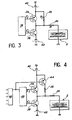
- the circuit shown in FIG. 3 supplies an electrolytic display cell 2 and it includes a resistor 30 of value R, a leakage resistance 32, of value R f much greater than R, a transistor 34 of PNP type, a transistor 36 of NPN type, a control circuit 38 for these transistors, a voltage source 40 of value + V and a voltage source 42 of value -V.
- the transistor 34 is controlled by a signal carried by an erasure connection Ef connected to the base of the transistor.
- the transistor 36 is controlled by another signal conveyed by a write connection Ec, also connected to the base of the transistor.
- the circuit 38 applies to the connections Ef and Ec voltages equal to either + V or to -V, depending on whether one wishes to obtain a writing, erasing or storage period.
- the table below specifies the state of the control according to the applied voltages:
- resistor 32 of value R f results in the existence of a weak current of the order of V / A t , in the direction of erasure.
- Resistor 32 can optionally be replaced by a suitably sized transistor.
- the circuit shown in Figure 4 includes the same elements as that of the previous figure with, in addition, a transistor 44 which makes it possible to interrupt the leakage current in certain cases.
- the base of this transistor is joined to a decoder46, which supplies in known manner the control circuit 38.
- This decoder delivers voltage signals “1” or “0 to circuit 38 so that the latter delivers appropriate voltages on the Ef and Ec connections as described in the previous table.
- the circuit 46 delivers a "0 for an electrode which must be erased and a" 1 "for an electrode which must be written. In the illustrated case, the transistor 44 is blocked (and the leakage current is then interrupted) when the electrode is in the writing period.
- the circuit shown in the figure includes a resistor 50, erase transistors 52 and 54, a write transistor 56, two batteries 58 and 60 of about 1.5 V and two erase control connections Ef and Ec and writing.
- the emitter-base voltage drop of the erasing transistors 52 and 54 is approximately 0.4 V for a low emitter current, which leaves a voltage of approximately 0.7 on display 2.
- V which is slightly greater than the required voltage 0.7 V which is slightly greater than the voltage required for the electrochemical formation of iodine on the electrode.
- This erasing voltage can optionally be controlled by the impedance of a reference electrode placed in the cell, as described in French patent application EN 78 18 224 filed on June 19, 1978 and published under the number 2 432195.
Landscapes
- Physics & Mathematics (AREA)
- Nonlinear Science (AREA)
- General Physics & Mathematics (AREA)
- Optics & Photonics (AREA)
- Control Of Indicators Other Than Cathode Ray Tubes (AREA)
- Electrochromic Elements, Electrophoresis, Or Variable Reflection Or Absorption Elements (AREA)
- Electrolytic Production Of Metals (AREA)
- Electrolytic Production Of Non-Metals, Compounds, Apparatuses Therefor (AREA)
- Devices For Indicating Variable Information By Combining Individual Elements (AREA)
Priority Applications (1)
| Application Number | Priority Date | Filing Date | Title |
|---|---|---|---|
| AT79400383T ATE91T1 (de) | 1978-06-19 | 1979-06-12 | Verfahren und schaltungsanordnung zur ansteuerung einer elektrolytischen anzeigezelle unter anwendung eines leckstroms fuer die loeschung. |
Applications Claiming Priority (2)
| Application Number | Priority Date | Filing Date | Title |
|---|---|---|---|
| FR7818222A FR2434449A1 (fr) | 1978-06-19 | 1978-06-19 | Procede de commande d'une cellule d'affichage electrolytique utilisant un courant de fuite pour l'effacement et circuit mettant en oeuvre ce procede |
| FR7818222 | 1978-06-19 |
Publications (2)
| Publication Number | Publication Date |
|---|---|
| EP0006793A1 EP0006793A1 (fr) | 1980-01-09 |
| EP0006793B1 true EP0006793B1 (fr) | 1981-06-17 |
Family
ID=9209666
Family Applications (1)
| Application Number | Title | Priority Date | Filing Date |
|---|---|---|---|
| EP79400383A Expired EP0006793B1 (fr) | 1978-06-19 | 1979-06-12 | Procédé de commande d'une cellule d'affichage électrolytique utilisant un courant de fuite pour l'effacement et circuit mettant en oeuvre ce procédé |
Country Status (8)
| Country | Link |
|---|---|
| US (1) | US4279475A (OSRAM) |
| EP (1) | EP0006793B1 (OSRAM) |
| JP (1) | JPS554092A (OSRAM) |
| AT (1) | ATE91T1 (OSRAM) |
| CA (1) | CA1130939A (OSRAM) |
| DE (1) | DE2960422D1 (OSRAM) |
| ES (1) | ES482165A1 (OSRAM) |
| FR (1) | FR2434449A1 (OSRAM) |
Families Citing this family (8)
| Publication number | Priority date | Publication date | Assignee | Title |
|---|---|---|---|---|
| FR2618570B1 (fr) * | 1987-07-24 | 1990-10-19 | Warszawski Bernard | Procede de modulation de la lumiere |
| FR2618568B1 (fr) * | 1987-07-24 | 1992-04-17 | Warszawski Bernard | Procede de fabrication d'un dispositif pour la modulation de la lumiere |
| FR2618566B1 (fr) * | 1987-07-24 | 1992-04-17 | Warszawski Bernard | Cellule pour la modulation de la lumiere |
| FR2618569B1 (fr) * | 1987-07-24 | 1989-12-22 | Warszawski Bernard | Technique de fabrication d'un dispositif pour la modulation de la lumiere |
| FR2618571B1 (fr) * | 1987-07-24 | 1990-10-19 | Warszawski Bernard | Materiau pour la modulation de la lumiere et procedes de fabrication |
| GB2324883A (en) * | 1997-04-28 | 1998-11-04 | Wisconsin Label Corp | Self-powered electrochemical display cell with focused field |
| US5977773A (en) * | 1997-08-15 | 1999-11-02 | The United States Of America As Represented By The Administrator Of The National Aeronautics And Space Administration | Non-intrusive impedance-based cable tester |
| US6136468A (en) | 1998-08-25 | 2000-10-24 | Timer Technologies, Llc | Electrochemical cell with deferred assembly |
Family Cites Families (5)
| Publication number | Priority date | Publication date | Assignee | Title |
|---|---|---|---|---|
| CH585913A5 (OSRAM) * | 1974-01-31 | 1977-03-15 | Suisse Horlogerie | |
| JPS51140642A (en) * | 1975-05-29 | 1976-12-03 | Seiko Epson Corp | Driving circuit |
| SU534990A1 (ru) * | 1975-12-22 | 1978-08-05 | Латвинский Ордена Трудового Красного Знамени Государственный Университет Им.Петра Стучки | Устройство дл управлени электрохромным элементом |
| JPS5314598A (en) * | 1976-07-26 | 1978-02-09 | Sharp Corp | Memory regeneration method of electrochromic display device |
| FR2403611A1 (fr) * | 1977-09-15 | 1979-04-13 | Commissariat Energie Atomique | Procede de commande d'une cellule d'affichage electrolytique et circuit de mise en oeuvre |
-
1978
- 1978-06-19 FR FR7818222A patent/FR2434449A1/fr active Granted
-
1979
- 1979-06-12 DE DE7979400383T patent/DE2960422D1/de not_active Expired
- 1979-06-12 EP EP79400383A patent/EP0006793B1/fr not_active Expired
- 1979-06-12 AT AT79400383T patent/ATE91T1/de not_active IP Right Cessation
- 1979-06-13 US US06/048,180 patent/US4279475A/en not_active Expired - Lifetime
- 1979-06-18 CA CA329,985A patent/CA1130939A/en not_active Expired
- 1979-06-19 JP JP7639479A patent/JPS554092A/ja active Pending
- 1979-06-19 ES ES482165A patent/ES482165A1/es not_active Expired
Also Published As
| Publication number | Publication date |
|---|---|
| FR2434449B1 (OSRAM) | 1982-02-05 |
| JPS554092A (en) | 1980-01-12 |
| US4279475A (en) | 1981-07-21 |
| ES482165A1 (es) | 1980-08-16 |
| DE2960422D1 (en) | 1981-09-24 |
| EP0006793A1 (fr) | 1980-01-09 |
| FR2434449A1 (fr) | 1980-03-21 |
| CA1130939A (en) | 1982-08-31 |
| ATE91T1 (de) | 1981-07-15 |
Similar Documents
| Publication | Publication Date | Title |
|---|---|---|
| EP0080394B1 (fr) | Bascule bistable à stockage non volatil et à repositionnement statique | |
| FR2550361A1 (fr) | Microcalculateur a structure integree muni d'une memoire a acces aleatoire | |
| EP0006793A1 (fr) | Procédé de commande d'une cellule d'affichage électrolytique utilisant un courant de fuite pour l'effacement et circuit mettant en oeuvre ce procédé | |
| FR2537316A1 (fr) | Dispositif d'affichage a matrice | |
| WO1993019405A1 (fr) | Piece d'horlogerie comprenant une source d'energie constituee par une cellule photovoltaique | |
| FR2543726A1 (fr) | Cellule de memoire ram non volatile a transistors cmos a grille flottante commune | |
| WO2000065735A1 (fr) | Procede et dispositif d'alimentation electrique dans un appareil mobile | |
| FR2738386A1 (fr) | Procede et circuit de programmation et d'effacement d'une memoire | |
| FR2538138A1 (fr) | Systeme d'asservissement en temperature d'un dispositif thermo-actif | |
| EP0006794B1 (fr) | Procédé de commande d'une cellule d'affichage électrolytique et dispositif de mise en oeuvre | |
| FR2490346A1 (OSRAM) | ||
| EP0278832B1 (fr) | Circuit de lecture pour mémoire | |
| FR2799869A1 (fr) | Dispositif d'affichage a cristal liquide et son procede de fabrication | |
| FR2762708A1 (fr) | Procede de commande d'une cellule memoire et memoire non volatile programmable une seule fois en technologie cmos | |
| EP0601922B1 (fr) | Mémoire EEPROM organisée en mots de plusieurs bits | |
| EP0902437A1 (fr) | Circuit de génération d'une haute tension de programmation ou d'effacement d'un mémoire | |
| EP0543703A1 (fr) | Mémoire intégrée électriquement programmable à un seul transistor | |
| EP0006797A1 (fr) | Cellule d'affichage électrolytique à électrode de référence et à tension d'effacement asservie | |
| EP4009371A1 (fr) | Dispositif selecteur pour dispositif memoire de type resistif et procede de fabrication associe | |
| FR2549999A1 (fr) | Cellule de memoire du type ram comprenant un element de memoire non volatil electriquement programmable | |
| EP0006811A2 (fr) | Cellule d'affichage électrolytique à dépôt métallique et procédé pour éviter un appauvrissement en métal de certaines zones de la contre-électrode d'une telle cellule | |
| CH616244A5 (OSRAM) | ||
| CH686599B5 (fr) | Pièce d'horlogerie alimentée par des cellules solaires. | |
| EP0080396A1 (fr) | Circuit téléphonique, géré par microprocesseur à circuit intégré de transmission 2 fils-4 fils, et alimentation de sauvegarde par courant de ligne | |
| EP0838824B1 (fr) | Mémoire à temps de lecture amélioré |
Legal Events
| Date | Code | Title | Description |
|---|---|---|---|
| PUAI | Public reference made under article 153(3) epc to a published international application that has entered the european phase |
Free format text: ORIGINAL CODE: 0009012 |
|
| AK | Designated contracting states |
Designated state(s): AT CH DE GB IT NL SE |
|
| 17P | Request for examination filed | ||
| ITF | It: translation for a ep patent filed | ||
| GRAA | (expected) grant |
Free format text: ORIGINAL CODE: 0009210 |
|
| AK | Designated contracting states |
Designated state(s): AT CH DE GB IT NL SE |
|
| REF | Corresponds to: |
Ref document number: 91 Country of ref document: AT Date of ref document: 19810715 Kind code of ref document: T |
|
| REF | Corresponds to: |
Ref document number: 2960422 Country of ref document: DE Date of ref document: 19810924 |
|
| PGFP | Annual fee paid to national office [announced via postgrant information from national office to epo] |
Ref country code: DE Payment date: 19840526 Year of fee payment: 6 |
|
| PGFP | Annual fee paid to national office [announced via postgrant information from national office to epo] |
Ref country code: CH Payment date: 19840606 Year of fee payment: 6 |
|
| PGFP | Annual fee paid to national office [announced via postgrant information from national office to epo] |
Ref country code: AT Payment date: 19840614 Year of fee payment: 6 |
|
| PGFP | Annual fee paid to national office [announced via postgrant information from national office to epo] |
Ref country code: SE Payment date: 19840630 Year of fee payment: 6 Ref country code: NL Payment date: 19840630 Year of fee payment: 6 |
|
| PG25 | Lapsed in a contracting state [announced via postgrant information from national office to epo] |
Ref country code: AT Effective date: 19850612 |
|
| PG25 | Lapsed in a contracting state [announced via postgrant information from national office to epo] |
Ref country code: SE Effective date: 19850613 |
|
| PG25 | Lapsed in a contracting state [announced via postgrant information from national office to epo] |
Ref country code: CH Effective date: 19850630 |
|
| PG25 | Lapsed in a contracting state [announced via postgrant information from national office to epo] |
Ref country code: NL Effective date: 19860101 |
|
| GBPC | Gb: european patent ceased through non-payment of renewal fee | ||
| REG | Reference to a national code |
Ref country code: CH Ref legal event code: PL |
|
| PG25 | Lapsed in a contracting state [announced via postgrant information from national office to epo] |
Ref country code: DE Effective date: 19860301 |
|
| NLV4 | Nl: lapsed or anulled due to non-payment of the annual fee | ||
| PG25 | Lapsed in a contracting state [announced via postgrant information from national office to epo] |
Ref country code: GB Effective date: 19881118 |
|
| EUG | Se: european patent has lapsed |
Ref document number: 79400383.0 Effective date: 19860728 |
|
| PLBE | No opposition filed within time limit |
Free format text: ORIGINAL CODE: 0009261 |
|
| STAA | Information on the status of an ep patent application or granted ep patent |
Free format text: STATUS: NO OPPOSITION FILED WITHIN TIME LIMIT |