EP0006725B1 - Elektrischer Verbinder zum Verbinden einer Flachleitung mit einem Substrat - Google Patents
Elektrischer Verbinder zum Verbinden einer Flachleitung mit einem Substrat Download PDFInfo
- Publication number
- EP0006725B1 EP0006725B1 EP79301163A EP79301163A EP0006725B1 EP 0006725 B1 EP0006725 B1 EP 0006725B1 EP 79301163 A EP79301163 A EP 79301163A EP 79301163 A EP79301163 A EP 79301163A EP 0006725 B1 EP0006725 B1 EP 0006725B1
- Authority
- EP
- European Patent Office
- Prior art keywords
- fingers
- substrate
- connector
- body portion
- conductors
- Prior art date
- Legal status (The legal status is an assumption and is not a legal conclusion. Google has not performed a legal analysis and makes no representation as to the accuracy of the status listed.)
- Expired
Links
Images
Classifications
-
- H—ELECTRICITY
- H01—ELECTRIC ELEMENTS
- H01R—ELECTRICALLY-CONDUCTIVE CONNECTIONS; STRUCTURAL ASSOCIATIONS OF A PLURALITY OF MUTUALLY-INSULATED ELECTRICAL CONNECTING ELEMENTS; COUPLING DEVICES; CURRENT COLLECTORS
- H01R12/00—Structural associations of a plurality of mutually-insulated electrical connecting elements, specially adapted for printed circuits, e.g. printed circuit boards [PCB], flat or ribbon cables, or like generally planar structures, e.g. terminal strips, terminal blocks; Coupling devices specially adapted for printed circuits, flat or ribbon cables, or like generally planar structures; Terminals specially adapted for contact with, or insertion into, printed circuits, flat or ribbon cables, or like generally planar structures
- H01R12/70—Coupling devices
- H01R12/82—Coupling devices connected with low or zero insertion force
- H01R12/85—Coupling devices connected with low or zero insertion force contact pressure producing means, contacts activated after insertion of printed circuits or like structures
- H01R12/88—Coupling devices connected with low or zero insertion force contact pressure producing means, contacts activated after insertion of printed circuits or like structures acting manually by rotating or pivoting connector housing parts
-
- H—ELECTRICITY
- H01—ELECTRIC ELEMENTS
- H01R—ELECTRICALLY-CONDUCTIVE CONNECTIONS; STRUCTURAL ASSOCIATIONS OF A PLURALITY OF MUTUALLY-INSULATED ELECTRICAL CONNECTING ELEMENTS; COUPLING DEVICES; CURRENT COLLECTORS
- H01R12/00—Structural associations of a plurality of mutually-insulated electrical connecting elements, specially adapted for printed circuits, e.g. printed circuit boards [PCB], flat or ribbon cables, or like generally planar structures, e.g. terminal strips, terminal blocks; Coupling devices specially adapted for printed circuits, flat or ribbon cables, or like generally planar structures; Terminals specially adapted for contact with, or insertion into, printed circuits, flat or ribbon cables, or like generally planar structures
- H01R12/70—Coupling devices
- H01R12/77—Coupling devices for flexible printed circuits, flat or ribbon cables or like structures
- H01R12/79—Coupling devices for flexible printed circuits, flat or ribbon cables or like structures connecting to rigid printed circuits or like structures
-
- H—ELECTRICITY
- H01—ELECTRIC ELEMENTS
- H01R—ELECTRICALLY-CONDUCTIVE CONNECTIONS; STRUCTURAL ASSOCIATIONS OF A PLURALITY OF MUTUALLY-INSULATED ELECTRICAL CONNECTING ELEMENTS; COUPLING DEVICES; CURRENT COLLECTORS
- H01R13/00—Details of coupling devices of the kinds covered by groups H01R12/70 or H01R24/00 - H01R33/00
- H01R13/58—Means for relieving strain on wire connection, e.g. cord grip, for avoiding loosening of connections between wires and terminals within a coupling device terminating a cable
-
- H—ELECTRICITY
- H01—ELECTRIC ELEMENTS
- H01R—ELECTRICALLY-CONDUCTIVE CONNECTIONS; STRUCTURAL ASSOCIATIONS OF A PLURALITY OF MUTUALLY-INSULATED ELECTRICAL CONNECTING ELEMENTS; COUPLING DEVICES; CURRENT COLLECTORS
- H01R13/00—Details of coupling devices of the kinds covered by groups H01R12/70 or H01R24/00 - H01R33/00
- H01R13/62—Means for facilitating engagement or disengagement of coupling parts or for holding them in engagement
- H01R13/627—Snap or like fastening
-
- H—ELECTRICITY
- H05—ELECTRIC TECHNIQUES NOT OTHERWISE PROVIDED FOR
- H05K—PRINTED CIRCUITS; CASINGS OR CONSTRUCTIONAL DETAILS OF ELECTRIC APPARATUS; MANUFACTURE OF ASSEMBLAGES OF ELECTRICAL COMPONENTS
- H05K3/00—Apparatus or processes for manufacturing printed circuits
- H05K3/36—Assembling printed circuits with other printed circuits
- H05K3/361—Assembling flexible printed circuits with other printed circuits
- H05K3/365—Assembling flexible printed circuits with other printed circuits by abutting, i.e. without alloying process
Definitions
- This invention relates to an electrical connector, and particularly an electrical connector for use in establishing electrical connections between the conductors of a flat multi-conductor electrical cable and conductors carried by a substrate.
- Such a connector is disclosed in French Patent Application No. 73.14613, publication No. FR-A-2241888, which discloses a connector comprising a single member stamped and formed from sheet metal and having an elongate body portion, a plurality of resilient contact fingers arranged in a row extending lengthwise of the body portion, all the fingers extending in the same direction and having their longitudinal axes extending transversely of the row direction, and mounting means formed at each end of the body portion and adapted and arranged to secure the connector to a substrate with the fingers extending towards and engaging conductors carried by the substrate.
- the fingers are arranged to point away from the edge of the substrate at which the connector is to be mounted, that is towards the cable to be connected to the substrate, and thus the connector can be mounted only at an edge of a substrate with the cable and connector being simultaneously applied to the substrate with the mounting means of the connector entering slots open to the edge of the substrate. This is because if the connector is first mounted onto the substrate without the cable, then the end of cable cannot subsequently be inserted between the fingers and the substrate since the free ends of the fingers are directed towards the cable and are in engagement with the substrate.
- This known connector thus has the disadvantages that as disclosed it can be used only at an edge of a substrate, and must be assembled to a substrate simultaneously with a cable, and must also be removed from the substrate when the cable is to be removed.
- U.S. Patent Specification No. US-A-3629787 discloses an electrical connector which serves the same purpose as the connector discussed above, and which comprises a housing of insulating material adapted to be secured to an end of a substrate having conductors on a surface thereof, the housing containing a contact structure stamped and formed from sheet metal and comprising a plurality of resilient fingers extending from one edge of a body portion, the fingers being reversely bent to underlie the body portion.
- the housing is secured to the substrate with exposed end portions of the conductors of a cable as described above positioned between the conductors on the substrate and the fingers such that the fingers are compressed and serve to urge the cable conductors into engagement with the substrate conductors to provide the required connections.
- This known connector has the disadvantages that it consists of a plurality of different parts which must be assembled together, and that no provision is made for zero force insertion of a cable end between the fingers and the substrate if the connector is mounted on the substrate prior to insertion of the cable end.
- an electrical connector for use in establishing electrical connections between the conductors of a flat multi-conductor electrical cable and conductors carried by a substrate
- the connector comprising a single member stamped and formed from sheet metal and having an elongate body portion, a plurality of resilient contact fingers arranged in a row extending lengthwise of the body portion, all the fingers extending in the same direction and having their longitudinal axes extending transversely of the row direction, and mounting means formed at each end of the body portion and adapted and arranged to secure the connector to a substrate with the fingers extending towards and engaging conductors carried by the substrate, characterised in that the fingers extend from one longitudinal edge of the body portion and are reversely bent to underlie the body portion, each finger being bent to present a rounded surface in a direction away from the body portion for engagement with a conductor carried by the substrate, and is then extended to provide a tail portion which, when the connector is mounted on the substrate extends in a spaced relationship from the substrate, the mounting means being formed on
- the connector of this invention has the advantages that it is cheap and simple to manufacture, can easily be mounted on a substrate at any required position not needing to be at an edge of the substrate, provides for zero force insertion of a cable end between the fingers and a substrate on which the connector is mounted, and does not have to be disassembled in any way when the cable is to be removed.
- U.S. Patent Specification No. US-A 3082398 discloses a contact finger structure somewhat similar in appearance to that of the connector of this invention.
- the finger structure of this prior specification is not used in the manner of the connector of this invention to provide zero force connection of a flat cable to conductors on a substrate, but is used supported by an insulating body and with a flat cable wrapped about the structure to provide a spring plug arrangement.
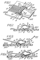
- the connector 1 shown in Figures 1 and 2 comprises a single member stamped and formed from sheet metal and having an elongate body portion 2 formed with a longitudinally extending strengthening embossment 3.
- a plurality of resilient contact fingers 4 extend from one longitudinal edge 5 of the body portion 2, the fingers 4 being in a row extending lengthwise of the body portion 2 with all the fingers 4 extending in the same direction and having their longitudinal axes extending transversely of the row direction.
- Each finger 4 is reversely bent to underlie the body portion 2, as clearly shown in Figure 2.
- Each end of the body portion 2 is formed with mounting means in the form of a flange 6 extending from the end of the body portion 2 and to the same side of the body portion 2 as the fingers 4, the free edge of the flange 6 remote from the body portion 2 being formed with two tabs 7.
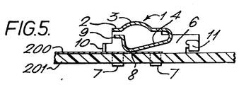
- Figure 1 shows the connector 1 in use in establishing connections between the conductors 100 of a flat multi-conductor electrical cable 101 in which the conductors 100 are encased in a sheet of insulating material 102, and conductors 200 on a substrate 201 such as a printed circuit board.
- the connector 1 is mounted on the substrate 201 by the tabs 7 being passed through respective holes in the substrate 201 and then being bent to engage the surface of the substrate 201 remote from the surface carrying the conductors 200, as shown in Figure 2, the free edges of the flanges 6 engaging the substrate 201.
- the fingers 4 resiliently engage respective conductors 200 on the substrate 201, as shown in Figure 2.
- the free end of each finger 4 is bent back towards the body portion 2 to present a rounded surface 8 to the substrate 201, and is then bent again to provide a short tail portion 9 which, when the connector 1 is mounted on the substrate 201, extends substantially parallel to and spaced from the surface of the substrate 201.
- End portions 10 of the flanges 6 adjacent the free ends of the fingers 4 are bent inwardly towards each other, and serve as pivot points for a tool 300 such as a sheet of metal, which is inserted under the tail portions 9 of the fingers 4 and over the pivot points 10 as shown in Figure 3.
- a tool 300 such as a sheet of metal
- Pressure on the outer end of the tool 300 towards the substrate 201 causes the tool 300 to lift the fingers 4 out of engagement with the conductors 200 on the substrate 201, as shown in Figure 4, whereby the treated end portion 103 of the cable 101 can be inserted between the fingers 4 and the conductors 200, with the exposed conductors 100 of the cable 101 facing and respectively aligned with the conductors 200.
- the tool 300 is then removed, and the fingers 4 resiliently engage the still insulated side of the end portion 103 of the cable 101 and urge the conductors 100 of the cable 101 into electrical contact with respective ones of the conductors 200 on the substrate 201.
- the fingers 4 and associated conductors 200 on the substrate 201 together define a tapering insertion mouth for the cable end portion 103 which can therefore be just pushed in between the fingers 4 and conductors 200, moving the fingers 4 as necessary during such insertion.
- Portions of the flanges 6 of the connector at the ends of the flanges 6 adjacent the roots of the fingers 4 are bent first inwardly towards each other and then bent again to extend away from the substrate 201 to provide hook portions 11 facing the fingers 4.
- the cable 101 has two holes 104 (Figure 1) formed therein, the holes 104 being positioned to receive the hook portions 11 of the connector 1 when the cable is inserted between the fingers 4 and the substrate 201, as shown in Figure 1, thereby to restrain the cable 101 from being pulled from the connector 1.
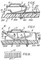
- the connector 1 here shown is similar to that shown in Figures 1 to 4, the only difference being that the fingers 4 are overall longer, and are such that the tail portion 9 of each finger 4 is positioned to limit the possible deflection of the finger 4 towards the body portion 2 to an extent ensuring that the finger cannot be overstressed such that the resiliency properties thereof are damaged.
- the connector 1 shown in Figure 6 is the same as that shown in Figures 1 to 4 save for a difference in the shape of the strengthening embossment 3. However, the connector 1 is shown mounted on the side of the substrate 201 remote from the conductors 200 carried by the substrate 201. In this assembly connections between the conductors 200 on the substrate and the conductors 100 of the cable 101 are established by way of L-shaped contact members 500 each having one limb extending across the surface of the substrate 201 on which the connector 1 is mounted, and the other limb extending through a hole in the substrate 201 and connected as by solder to a respective conductor 200. The fingers 4 of the connector 1 serve to urge the conductors 100 of the cable 101 into engagement with respective ones of the contact members 500 whereby the required connections are established.
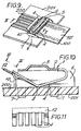
- the connector 1 here shown is similar to that shown in the Figure 6 assembly, save that the strain relief hook portions 11 are omitted, and the fingers 4 are of such a length to extend beyond the body portion 2 so as to be accessible to the hand of a user of the connector. Further, as shown in Figure 8, the "free" ends of the fingers 4 are joined by an integrally formed cross-member 12.
- the connector here shown is similar to that shown in Figures 1 to 4 save that the hook portions 11 are omitted, and the fingers 4 are of such a length to extend beyond the body portion 2 of the connector 1.
- the connector 1 also includes a cross-member 12 similar to that shown in Figures 7 and 8, the difference being that this cross-member is joined to the "free" ends of only the end fingers 4, which end fingers 4 are bent, as shown in Figure 10, such that the cross-member 12 engages under the free ends of the remaining fingers 4, as clearly shown in Figure 11.
- the fingers 4 can be lifted out of engagement with the substrate 201 by manual action on the cross-member 12, for insertion of a cable between the fingers 4 and the substrate 201.
Claims (5)
Priority Applications (1)
| Application Number | Priority Date | Filing Date | Title |
|---|---|---|---|
| AT79301163T ATE2035T1 (de) | 1978-06-22 | 1979-06-18 | Elektrischer verbinder zum verbinden einer flachleitung mit einem substrat. |
Applications Claiming Priority (8)
| Application Number | Priority Date | Filing Date | Title |
|---|---|---|---|
| US918139 | 1978-06-22 | ||
| US05/918,139 US4172626A (en) | 1978-06-22 | 1978-06-22 | Connector clip for connecting cable conductors to circuit board conductors |
| US953677 | 1978-10-23 | ||
| US05/953,677 US4181386A (en) | 1978-06-22 | 1978-10-23 | Zero insertion force connector clip |
| US1686479A | 1979-03-02 | 1979-03-02 | |
| US16864 | 1979-03-02 | ||
| US24356 | 1979-03-27 | ||
| US06/024,356 US4252389A (en) | 1979-03-27 | 1979-03-27 | Zero insertion force connector having integral unloading means |
Publications (2)
| Publication Number | Publication Date |
|---|---|
| EP0006725A1 EP0006725A1 (de) | 1980-01-09 |
| EP0006725B1 true EP0006725B1 (de) | 1982-12-15 |
Family
ID=27486609
Family Applications (1)
| Application Number | Title | Priority Date | Filing Date |
|---|---|---|---|
| EP79301163A Expired EP0006725B1 (de) | 1978-06-22 | 1979-06-18 | Elektrischer Verbinder zum Verbinden einer Flachleitung mit einem Substrat |
Country Status (9)
| Country | Link |
|---|---|
| EP (1) | EP0006725B1 (de) |
| AR (1) | AR217931A1 (de) |
| BR (1) | BR7903646A (de) |
| CA (1) | CA1122285A (de) |
| DE (1) | DE2964261D1 (de) |
| DK (1) | DK148209C (de) |
| ES (1) | ES481638A1 (de) |
| FI (1) | FI65870C (de) |
| NO (1) | NO148905C (de) |
Families Citing this family (6)
| Publication number | Priority date | Publication date | Assignee | Title |
|---|---|---|---|---|
| DE3245521C2 (de) * | 1982-12-09 | 1986-05-07 | Preh, Elektrofeinmechanische Werke Jakob Preh Nachf. Gmbh & Co, 8740 Bad Neustadt | Mehrpolige Randverbinderleiste |
| CH655203A5 (fr) * | 1984-01-19 | 1986-03-27 | Battelle Memorial Institute | Connecteur electrique d'un module a circuit electronique. |
| CH665059A5 (fr) * | 1985-04-03 | 1988-04-15 | Rdi Limited Partnership | Ensemble englobant un circuit modulaire electrique ou electronique et un connecteur destine a relier le circuit a un systeme electrique autonome. |
| GB2222959A (en) * | 1988-09-16 | 1990-03-28 | Takara Co Ltd | Movable decorative article |
| GB2255688B (en) * | 1991-05-10 | 1994-11-23 | Northern Telecom Ltd | Telephone station set with flexible and rigid circuit boards |
| JP3993828B2 (ja) * | 2003-01-23 | 2007-10-17 | 株式会社アドバンストシステムズジャパン | Fpc接続用マイクロコネクタ |
Family Cites Families (8)
| Publication number | Priority date | Publication date | Assignee | Title |
|---|---|---|---|---|
| US3082398A (en) * | 1960-05-24 | 1963-03-19 | Amphenol Borg Electronics Corp | Electrical connectors |
| US3141720A (en) * | 1961-09-22 | 1964-07-21 | James G Johnson | Connector for printed or etched flat conductor cables |
| US3492538A (en) * | 1967-09-07 | 1970-01-27 | Thomas & Betts Corp | Removable stack interconnection system |
| US3629787A (en) * | 1970-06-19 | 1971-12-21 | Bell Telephone Labor Inc | Connector for flexible circuitry |
| GB1376644A (en) * | 1972-05-20 | 1974-12-11 | Ford Motor Co | Electrical conductor assembly |
| GB1430769A (en) * | 1972-10-27 | 1976-04-07 | Kbl Eng Stapleford Ltd | Method of and means for establishing an electrical connection between a flexible conductor cable or strip and a rigid circuit board |
| FR2241888B1 (de) * | 1973-04-20 | 1976-04-23 | Mecanique Ind Int | |
| US4054348A (en) * | 1976-07-29 | 1977-10-18 | Ncr Corporation | Electrical connector |
-
1979
- 1979-06-07 CA CA000329233A patent/CA1122285A/en not_active Expired
- 1979-06-07 NO NO791896A patent/NO148905C/no unknown
- 1979-06-08 BR BR7903646A patent/BR7903646A/pt not_active IP Right Cessation
- 1979-06-18 EP EP79301163A patent/EP0006725B1/de not_active Expired
- 1979-06-18 DE DE7979301163T patent/DE2964261D1/de not_active Expired
- 1979-06-18 ES ES481638A patent/ES481638A1/es not_active Expired
- 1979-06-20 FI FI791973A patent/FI65870C/fi not_active IP Right Cessation
- 1979-06-21 DK DK260379A patent/DK148209C/da not_active IP Right Cessation
- 1979-06-22 AR AR277008A patent/AR217931A1/es active
Also Published As
| Publication number | Publication date |
|---|---|
| EP0006725A1 (de) | 1980-01-09 |
| NO148905C (no) | 1984-01-04 |
| DK260379A (da) | 1979-12-23 |
| ES481638A1 (es) | 1980-01-16 |
| DK148209C (da) | 1985-09-23 |
| DE2964261D1 (en) | 1983-01-20 |
| FI65870B (fi) | 1984-03-30 |
| DK148209B (da) | 1985-04-29 |
| NO148905B (no) | 1983-09-26 |
| FI791973A (fi) | 1979-12-23 |
| FI65870C (fi) | 1984-07-10 |
| AR217931A1 (es) | 1980-04-30 |
| CA1122285A (en) | 1982-04-20 |
| BR7903646A (pt) | 1980-02-05 |
| NO791896L (no) | 1979-12-28 |
Similar Documents
| Publication | Publication Date | Title |
|---|---|---|
| US4009921A (en) | Electrical contact and support means therefor | |
| US5588884A (en) | Stamped and formed contacts for a power connector | |
| US4191440A (en) | Electrical connector for coupling power leads to circuit boards | |
| KR100280992B1 (ko) | 암형 전기 단자 | |
| CA1084134A (en) | Electrical connector contact clip | |
| WO2003028160A3 (en) | High current automotive electrical connector and terminal | |
| EP0393058A1 (de) | Elektrisches aufnahmeendstück. | |
| JPH0160908B2 (de) | ||
| EP0966062B1 (de) | Schneidklemmbuchsenkontakt mit hoher Haltekraft | |
| JPS5553882A (en) | Device for connecting flat cable | |
| US4648678A (en) | Electrical connector | |
| EP0000088A1 (de) | Steckverbinder mit Zugentlastungsdeckel für Flachkabel | |
| US5344338A (en) | Strain relief structure for connecting flat flexible cable to a circuit board | |
| US4886942A (en) | Strain relief structure for connecting flat flexible cable to a circuit board | |
| US3960425A (en) | Harness cable connector | |
| US5167544A (en) | Female electrical contact | |
| EP0006725B1 (de) | Elektrischer Verbinder zum Verbinden einer Flachleitung mit einem Substrat | |
| EP0109297B1 (de) | Elektrische Kontaktorgane und Zusammenbau elektrischer Verbinder | |
| EP0026568B1 (de) | Stecker zum Verbinden von Leitern eines Flachkabels mit Leiterbahnen auf einem Substrat | |
| US4957453A (en) | Electrical socket | |
| US4358172A (en) | Connector for electrical interconnection of circuit board and flat multiconductor cable | |
| EP0065357A1 (de) | Steckverbinder mit einer schwachen Einführkraft | |
| US4522460A (en) | Connecting means for closely spaced conductors | |
| JPH0338706B2 (de) | ||
| US4449773A (en) | Low insertion force connector |
Legal Events
| Date | Code | Title | Description |
|---|---|---|---|
| PUAI | Public reference made under article 153(3) epc to a published international application that has entered the european phase |
Free format text: ORIGINAL CODE: 0009012 |
|
| AK | Designated contracting states |
Designated state(s): AT BE CH DE FR GB IT NL SE |
|
| 17P | Request for examination filed | ||
| ITF | It: translation for a ep patent filed |
Owner name: BARZANO' E ZANARDO MILANO S.P.A. |
|
| GRAA | (expected) grant |
Free format text: ORIGINAL CODE: 0009210 |
|
| AK | Designated contracting states |
Designated state(s): AT BE CH DE FR GB IT NL SE |
|
| REF | Corresponds to: |
Ref document number: 2035 Country of ref document: AT Date of ref document: 19821215 Kind code of ref document: T |
|
| REF | Corresponds to: |
Ref document number: 2964261 Country of ref document: DE Date of ref document: 19830120 |
|
| ET | Fr: translation filed | ||
| PGFP | Annual fee paid to national office [announced via postgrant information from national office to epo] |
Ref country code: SE Payment date: 19840630 Year of fee payment: 6 |
|
| PG25 | Lapsed in a contracting state [announced via postgrant information from national office to epo] |
Ref country code: SE Effective date: 19860619 |
|
| PGFP | Annual fee paid to national office [announced via postgrant information from national office to epo] |
Ref country code: DE Payment date: 19930503 Year of fee payment: 15 |
|
| PGFP | Annual fee paid to national office [announced via postgrant information from national office to epo] |
Ref country code: FR Payment date: 19930510 Year of fee payment: 15 |
|
| PGFP | Annual fee paid to national office [announced via postgrant information from national office to epo] |
Ref country code: AT Payment date: 19930513 Year of fee payment: 15 |
|
| PGFP | Annual fee paid to national office [announced via postgrant information from national office to epo] |
Ref country code: BE Payment date: 19930527 Year of fee payment: 15 |
|
| PGFP | Annual fee paid to national office [announced via postgrant information from national office to epo] |
Ref country code: CH Payment date: 19930623 Year of fee payment: 15 |
|
| ITTA | It: last paid annual fee | ||
| PGFP | Annual fee paid to national office [announced via postgrant information from national office to epo] |
Ref country code: NL Payment date: 19930630 Year of fee payment: 15 |
|
| REG | Reference to a national code |
Ref country code: GB Ref legal event code: 732E |
|
| PGFP | Annual fee paid to national office [announced via postgrant information from national office to epo] |
Ref country code: GB Payment date: 19940519 Year of fee payment: 16 |
|
| PG25 | Lapsed in a contracting state [announced via postgrant information from national office to epo] |
Ref country code: AT Effective date: 19940618 |
|
| PG25 | Lapsed in a contracting state [announced via postgrant information from national office to epo] |
Ref country code: CH Effective date: 19940630 Ref country code: BE Effective date: 19940630 |
|
| BERE | Be: lapsed |
Owner name: AMP INC. (UNE SOC. DE PENNSYLVANIE) Effective date: 19940630 |
|
| PG25 | Lapsed in a contracting state [announced via postgrant information from national office to epo] |
Ref country code: NL Effective date: 19950101 |
|
| EUG | Se: european patent has lapsed |
Ref document number: 79301163.6 Effective date: 19870504 |
|
| NLV4 | Nl: lapsed or anulled due to non-payment of the annual fee | ||
| PG25 | Lapsed in a contracting state [announced via postgrant information from national office to epo] |
Ref country code: FR Effective date: 19950228 |
|
| REG | Reference to a national code |
Ref country code: CH Ref legal event code: PL |
|
| PG25 | Lapsed in a contracting state [announced via postgrant information from national office to epo] |
Ref country code: DE Effective date: 19950301 |
|
| REG | Reference to a national code |
Ref country code: FR Ref legal event code: ST |
|
| PG25 | Lapsed in a contracting state [announced via postgrant information from national office to epo] |
Ref country code: GB Effective date: 19950618 |
|
| GBPC | Gb: european patent ceased through non-payment of renewal fee |
Effective date: 19950618 |
|
| PLBE | No opposition filed within time limit |
Free format text: ORIGINAL CODE: 0009261 |
|
| STAA | Information on the status of an ep patent application or granted ep patent |
Free format text: STATUS: NO OPPOSITION FILED WITHIN TIME LIMIT |