EP0002138A1 - Programmiergerät für ein Steuergerät für elektrische Systeme und Apparate - Google Patents
Programmiergerät für ein Steuergerät für elektrische Systeme und Apparate Download PDFInfo
- Publication number
- EP0002138A1 EP0002138A1 EP78300655A EP78300655A EP0002138A1 EP 0002138 A1 EP0002138 A1 EP 0002138A1 EP 78300655 A EP78300655 A EP 78300655A EP 78300655 A EP78300655 A EP 78300655A EP 0002138 A1 EP0002138 A1 EP 0002138A1
- Authority
- EP
- European Patent Office
- Prior art keywords
- memory
- counter
- contact
- output
- manually
- Prior art date
- Legal status (The legal status is an assumption and is not a legal conclusion. Google has not performed a legal analysis and makes no representation as to the accuracy of the status listed.)
- Granted
Links
- 230000015654 memory Effects 0.000 claims abstract description 185
- 238000010586 diagram Methods 0.000 claims abstract description 43
- 238000013500 data storage Methods 0.000 claims abstract 2
- 230000006870 function Effects 0.000 claims description 12
- 230000004044 response Effects 0.000 claims description 5
- 239000000872 buffer Substances 0.000 description 22
- 239000004020 conductor Substances 0.000 description 22
- 239000003990 capacitor Substances 0.000 description 17
- 230000009471 action Effects 0.000 description 14
- 230000002441 reversible effect Effects 0.000 description 13
- 230000036961 partial effect Effects 0.000 description 7
- 238000000034 method Methods 0.000 description 5
- 230000007704 transition Effects 0.000 description 5
- 230000000694 effects Effects 0.000 description 4
- 230000000670 limiting effect Effects 0.000 description 3
- 230000000903 blocking effect Effects 0.000 description 2
- 230000008859 change Effects 0.000 description 2
- 238000012423 maintenance Methods 0.000 description 2
- 230000000717 retained effect Effects 0.000 description 2
- 238000005096 rolling process Methods 0.000 description 2
- FGRBYDKOBBBPOI-UHFFFAOYSA-N 10,10-dioxo-2-[4-(N-phenylanilino)phenyl]thioxanthen-9-one Chemical compound O=C1c2ccccc2S(=O)(=O)c2ccc(cc12)-c1ccc(cc1)N(c1ccccc1)c1ccccc1 FGRBYDKOBBBPOI-UHFFFAOYSA-N 0.000 description 1
- 241000596875 Gladiolus communis Species 0.000 description 1
- 230000008901 benefit Effects 0.000 description 1
- 230000002457 bidirectional effect Effects 0.000 description 1
- 230000008878 coupling Effects 0.000 description 1
- 238000010168 coupling process Methods 0.000 description 1
- 238000005859 coupling reaction Methods 0.000 description 1
- 230000002452 interceptive effect Effects 0.000 description 1
- 238000002372 labelling Methods 0.000 description 1
- 230000014759 maintenance of location Effects 0.000 description 1
- 239000002184 metal Substances 0.000 description 1
- 230000004048 modification Effects 0.000 description 1
- 238000012986 modification Methods 0.000 description 1
- 230000008569 process Effects 0.000 description 1
- 230000002829 reductive effect Effects 0.000 description 1
Images


Classifications
-
- G—PHYSICS
- G05—CONTROLLING; REGULATING
- G05B—CONTROL OR REGULATING SYSTEMS IN GENERAL; FUNCTIONAL ELEMENTS OF SUCH SYSTEMS; MONITORING OR TESTING ARRANGEMENTS FOR SUCH SYSTEMS OR ELEMENTS
- G05B19/00—Programme-control systems
- G05B19/02—Programme-control systems electric
- G05B19/04—Programme control other than numerical control, i.e. in sequence controllers or logic controllers
- G05B19/05—Programmable logic controllers, e.g. simulating logic interconnections of signals according to ladder diagrams or function charts
- G05B19/056—Programming the PLC
Definitions
- This invention relates to a control system in or for a controller for electrical circuit systems and apparatus, which controller is programmable with logic instructions representative of circuit nodes of a ladder diagram.
- the task of a programmable controller is to compute the logic status represented by interconnected contacts and to apply the end result of such logic computation to a coil to either energize or deenergize it or to send such result to the outside to control external devices such as solenoids, for example.
- the direction of logic is from the left hand vertical 110 volt A.C..power line flowing through the contacts and coils to the right hand vertical power line.
- the programmable controller emulates this action, but there are quite significant differences between the internal functions of the programmable controller and the relay system that it replaces. Among these are:
- the functions of programmable controllers can be actually grouped into three sections: (1) the input section consisting of the power source from line LI-L2 and connections through limit switches and pushbuttons to the input terminals of the controller; (2) the logic section based on internal processing resembling to a great degree computer-like functions; and (3) the output section where logic function results control external devices connected to the output terminals of the controller and power lines L1-L2.
- the logic task consists of determining the state of a signal coming from a set of interconnected contacts, based both on how the contacts are interconnected and the states of the individual contacts, open or closed.
- the logic action is: a logic signal will flow from left to right and be present at the "output” if, and only if, all three contacts are closed.
- This is the equivalent of an AND-logic operation, that is a logic " 1 " is obtained if Contact-1 and Contact-2 and Contact-3 are closed.
- Programmable controllers compute the logic represented by series and parallel contacts through sequential instructions placed into a memory. Each instruction has a portion indicating the type of operation to be performed, series or parallel, and a reference number defining where the internal processor is to go to find the status of the device (input or coil) controlling the contact. The programmer must determine and write these instructions according to the manner in which the contacts are interconnected.
- the procedure outlined is available in certain prior art large controllers and in at least one small controller.
- the large controllers provide cathod-ray tube diagram monitors which simplify the task of storing and retrieving temporary logic results.
- programming can become difficult without such aids when diagrams become complex, for the programmer must then keep track of a number of temporary results, storing and retrieving them as required. It is especially difficult for maintenance men to grasp the logic being performed by a list of instructions as given above. Accordingly, it is desirable to provide improved means that are simple and easy to program and does not require any diagram modification.
- An embodiment of the invention to be described herein is an improved control system in or for a controller for electrical circuit systems and apparatus, which controller is programmable with logic instructions representative of circuit nodes of a ladder diagram.
- the control,system includes a panel having a slot into which a memory board may be plugged and means for storing a wire number program in the memory.
- the panel includes a slot into which a memory board may be plugged and means for storing a ladder diagram program of multiplexed sets of instruction words in successively numbered address locations therein.
- the panel includes means for displaying the multiplexed sets of instruction words in decimal form and for displaying the address locations in decimal form.
- the panel is able to store the multiplexed sets of instruction words in binary-coded-decimal form and display them in decimal form. It is able to address the memory locations in binary form and display them in decimal form.
- the embodiment includes improved means for stepping a binary counter and a binary-coded-decimal counter in unison and for preventing the binary counter from stepping out of its count synchronism the BCD counter at its reverse recycle point.
- Improved means is provided for stepping an up-down binary counter and an up-down binary-coded-decimal counter in unison and for causing the binary counter to track the BCD counter forward and up to its reverse recycle point thereby to allow use of the binary counter for memory addressing and use of the BCD counter for decimal display of the memory locations.
- the embodiment includes a logic system which has bidirectional data terminals and means for displaying the instruction words stored in binary-coded-decimal form in the memory, means for using a binary bit of a contact instruction word as indicative of normally-open or normally-closed contact, and logic means for preventing inclusion of the N.O.-N.C. binary bit in the instruction word numerical value display.
- the panel has means for automatically storing in the memory a special blanking code of all 1's in a first predetermined location indicative of an OR-logic instruction whenever any contact but the last one of a plurality of parallel contacts is stored in the memory.
- the panel is able to automatically store in the memory a special blanking code of all 1's in a second predetermined location indicative of an output instruction whenever such output instruction or a coil instruction is stored in the memory.
- wire number programming The programming basis of this control system panel, as well as the programmable controller disclosed in the aforementioned copending application with which it may be used, is known as "wire number programming".
- the ladder diagram is provided with wire numbers as in a relay ladder diagram. Each wire number defines an interconnected portion of the circuit known as a circuit node.
- the instructions written by the control panel define the logic connected to each wire number as will hereinafter appear.
- the processor in the programmable controller determines the status of each wire number and maintains a complete record in a wire number memory incorporated for that purpose.
- this provides a particularly simple programming method for, in effect, the result of every logic operation is stored and the programmer does not have to pick and choose as well as to provide additional apparatus to keep track of what has been stored.
- the maintaining of wire number status also affords a powerful maintenance tool in that signal tracing is merely a matter of calling up wire number values from the memory of the controller.
- Wire number programming requires only two instructions, namely, (1) the contact instruction and (2) the output instruction.
- the contact instruction is written for each contact and consists of three parts: (a) the input wire number to the contact, (b) the contact reference number, and (c) the output wire number from the contact.
- the contact reference number additionally has a "bit" flagging the contact as normally-open or normally-closed.
- the instructions for three parallel contacts or contacts that connect to the same output wire number are written as follows: where Fl,F2 and F3 are the multiplexed time periods or fields, the 1's are input wire numbers to parallel contacts, 401-1 is a N.C. contact, 402-0 and 403-0 are N.O. contacts, and 5 is the output wire number to which all three contacts connect.
- the F3 sections of the first two instructions are left blank, although the output wire number 5 can be inserted if desired, for the programming panel will put a special code of all 1's in this section when the instruction is entered as "partial parallel" as hereinafter more fully described.
- the programmable controller Upon reading these instructions, the programmable controller will detect the special code and the results of these instructions will be OR'd until the final instruction when the result of the OR operations, including the final instruction, is stored in the wire number memory.
- the output instruction involves writing of only two sections F1 and F3.
- the input wire number connected to an output such as a control coil, latching coil, timing coil, or power output is entered in field Fl.
- the output element reference number is then entered into field F3.
- the programming panel automatically introduces the special code of all 1's into field F2, and this is used by the programmable controller to initiate an output action.
- the programming panel is used to generate a wire number program for the programmable controller disclosed in the aforementioned copending application.
- this program will consist of sets of instruction words for logic functions that will simulate the ladder diagram shown in Figure 1. These sets of instruction words or data will be written into the memory to be stored therein for subsequent use in running the programmable controller shown in the above copending application.
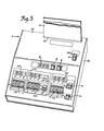
- the programming panel comprises an enclosure 2 of metal of the like having a top panel 2a attached to a frame 2b for housing and supporting the programming control logic circuits of Figures 7a-7e including the manual switches and indicators.
- the power supply circuit of Figure 7a and the logic circuits of Figures 7b-7e are arranged on PC boards and are mounted to the lower surface of top panel 2a.
- the power cord enters this panel 2 through a hole in the rear wall thereof and is connected through a fuse to "power on" switch 4.
- power on switch 4 is a double-pole single-throw type toggle switch for connecting A.C. power lines L1 and L2 to transformer T1 thereby to supply the operating power to the programming panel as hereinafter more fully described.
- a power-on indicator lamp LPO is mounted adjacent to power switch 4.
- the programming panel of Figure 5 also comprises three sets of bi-directional pushbutton selector switches F1S, F2S and F3S arranged from left to right with three switches in each set including a units switch U, a tens switch T and a hundreds switch H relatively located in the normal manner from the right to the left.
- these selector switches are arranged for setting up three three-digit decimal numbers in the process of programming the (1) input wire number to a contact, (2) the contact number and (3) the output wire number from the contact that are multiplexed into the memory during time periods or fields Fl,F2 and F3, respectively, as hereinafter more fully described.
- These selector switches are each provided with a pair of pushbuttons as shown in Figure 5 and a rotary decimal indicator visible through the window between the pushbuttons.
- the lower pushbutton advances the selector switch up from 0 to 9 one step each time the button is pressed, and the upper pushbutton reverses the selection similarly one step at a time from 9 to 0.
- These selector switches are of the decimal-to-BCD decoder type made by Durant Digital Instruments that are actuated on a decimal basis to provide a BCD (binary-coded-decimal) electrical output as shown in Figure 7d and 8.
- Each of these selector switches connects a common ground to BCD outputs 1,2,4 and 8 in the combinations shown in Figure 8 when the wheel indicator is set to a decimal value, except the hundreds digit H of switch F'2S wherein only BCD outputs 100,200 and 400 are used for numerical contact data and BCD output 800 is used as a bit to program and distinguish between a normally-open and a normally-closed contact.
- the programming panel is provided with a single-pole single-throw switch 6 shown in Figures 5 and 7d which programs a normally-open contact when it is open and which is closed to program a normally-closed contact.
- the programming panel is also provided with a "step" switch 8 of the single-pole double-throw momentary type shown in Figures 5 and 7b for stepping a program counter through the memory locations in either the forward or reverse (back) direction.
- a "step" switch 8 of the single-pole double-throw momentary type shown in Figures 5 and 7b for stepping a program counter through the memory locations in either the forward or reverse (back) direction.
- the number of that location O-255 is indicated on a 3-digit decimal indicator 10.
- a single-pole single-throw momentary switch 12 is located between forward/back step switch 8 and indicator 10 for "rolling" the program counter through the address locations of the memory, that is, advancing continuously in the forward direction under clock control as long as this switch is held closed, and displaying the locations on indicator 10.
- the programming panel is also provided with a pair of "enter" switches 14 and 16 shown in Figures 5 and 7b for entering into memory M the instruction data that has been set up on selector switches F1S,F2S and F3S.
- Switch 14 is a single-pole, double-throw momentary type having a center "off" position and a "partial parallels" position for entering the instructions regarding all except the last one of a plurality of contacts connected to the same output wire node, and a "series or last parallel” position for entering the instructions regarding series contacts and the last contact of a plurality of contacts connected to the same output wire node.
- Switch 16 is a single-pole single-throw momentary type having an off position and a "coil or output” position for entering the instructions regarding a control coil and an output from the ladder diagram.
- the programming panel is also provided with a connector socket 18 into which is plugged the PC board on which the memory to be programmed is mounted. After this memory has been programmed in accordance with a desired program, the memory PC board is unplugged therefrom and plugged into a programmable controller chassis such as shown in the above copending application preparatory to running the controller.
- the programming panel is further provided with three three-digit decimal indicators F 1 I,F2I and F3I directly above the respective sets of selector switches for indicating the data which is read as soon as it is entered in the main memory M.
- F 1 I,F2I and F3I Directly to the right of the F2I indicator are two lamps LP1 and LP2 for displaying the N.O. or N.C. state of the contact that has been programmed.
- this panel has symbols and legends that aid the person doing the programming in performing the necessary operations.
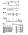
- Figure 1 shows a simple ladder diagram that will serve for illustrative purposes. As shown therein, the left vertical is numbered “1" and the wire nodes toward the right along the "rungs" starting from the top are numbered "2","3", etc. as is common practice in relay ladder diagrams.
- the programmable controller of the aforementioned copending application with which this programming panel may be used has a capacity for processing 1 ,000 wire numbers within a range of 0 to 999.
- the pushbuttons and lamp are I/O elements in the input-output section of the controller.
- the pushbuttons are numbered 003 and 004 and the lamp is numbered 020.
- the aforesaid controller has a capacity such that up to 400 such elements can be addressed in the I/O section over an address range of 000-399. This address range may overlap the wire number addess range because they are in different multiplexed time fields so that there will be no interference as will become apparent.
- the address range from 400-799 is used to address control coils in the control coil memory of the aforesaid controller.
- the control coil is numbered 400 and each of its two contacts is also numbered 400.
- the control coil memory is actually the equivalent of an input-output device but having a capacity of the equivalent of 400 control coils.
- One bit, Dll, in the control coil addressing word flags a N.O. or N.C. contact. If the contact is N.O., D1 1 is "O" and if the contact is N.C., Dll is "1".
- Use of bit "Dll" in control coil contact field F2 for this purpose limits the maximum F2 instruction to 799.
- FIG. 1 The ladder diagram configuration shown in Figure 1 is written into a program as shown in Figure 9.
- the left column shows the successive memory locations numbered in sequence from 000 to 005 and up to 255 if needed.
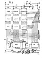
- Figure 6 shows nine HM-6562 memory chips of the 256 X 4 CMOS RAM type arranged in three columns CF1,CF2 and CF3 liaving three chips, 6462A-C,6562D-F and 6562G-1 in the respective columns. These columns of memory chips are identified as CFl,CF2 and CF3 to relate them to similarly identified multiplexed time slots Fl,F2 and F3 hereinafter for convenience.
- Each chip has four bits bi-directional output and 256 locations so that the three chips in parallel in each column receive and provide 12-bit words.
- column CF1 has a 12-bit word in location 000
- column CF2 has a 12-bit word in location 000
- column CF3 has a 12-bit word in location 000.
- the input wire number 001 shown in the second column of Figure 9 is stored in column CF1, location 000 of the memory in BCD form.
- the contact number 003 shown in the third column of Figure 9 is stored in column CF2, location 000 of the memory in BCD form along with one "O" bit Qll indicative of the N.O. character of the contact.
- the special code shown in the last column of Figure 10 is stored in column F3, location 000 of the memory. From this arrangement, it will be seen that the main memory can be addressed by multiplexing the same address in the three memory chip columns in sequence and then advancing to the next address.
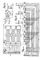
- Timing chart shown in Figure 10 This timing chart may be regarded as starting from the left edge of a clock pulse at time T1.
- a continuously running symmetrical oscillator, OSC in Figure 7b generates a clock signal CL and an inverted clock signal ICL.
- the clock signal is used for clocking the "roll" synchronizing flip-flop 4013A and the F' signal decoder 4555A in Figure 7b and for controlling the parity check memory 6508 in Figure 6 as hereinafter described.
- the inverted clock signal ICL goes negatively for the first half of each F period and positively for the second half thereof.
- the F periods are FO,Fl,F2 and F3 as indicated at the top of Figure 10 and repeat as shown therein.
- This inverted clock signal is used for running multiplexing binary counter 4024 which in turn also runs F decoder 4555B that produces the F periods referred to.
- This inverted clock signal also is used for clocking the write signal into the main memory.
- the next three signals Q1,Q2 and Q4 are the first, second and fourth outputs of binary counter 4024.
- Signals Q1 and Q2 are the two least significant bits (LSB's) of binary counter 4024 and are used to run the aforesaid F decoder 4555B and also F' decoder 4555A, and are also sent to the main memory for the purpose of developing chip enable multiplex signals that are needed in both writing and reading of the memory as hereinafter described.
- the ROLL signal Q4 is the 960 Hz inverted clock signal divided by 16 in counter 4024 to provide a 60 Hz ROLL clock for continuously advancing or "rolling" through the memory locations in order to quickly reach a desired memory location.
- the next four signals F0,F1,F2 and F3 in Figure 1 0 are the outputs of the aforesaid F decoder 4555B in Figure 7b that define the F fields or time periods shown at the top of Figure 10 and are used for multiplex switching of the program data from the selector switches to both the memory and display.
- the next four signals FO',F1',F2' and F3' are the outputs of the aforesaid F' decoder 4555A in Figure 7b controlled by clock CL and are used for performing timing operations in the programming logic circuit of Figures 7b-7e as hereinafter described.
- the next four signals IF0,IF1,IF2 and IF3 are the outputs of decoder 4556 in Figure 6 and are used for inhibit control (signal IFO) and for multiplex chip enable of the three main memory chip columns (signals IF 1 ,IF2 and IF3).
- the program instructions are first written as shown in the table in Figure 9. Then the power is turned on at switch 4 and the memory address counter which is the binary up-down counter in Figure 7c is automatically reset to the memory zero location by initial power on circuit IPO in Figure 7c. At the same time, the BCD up-down display counter in Figure 7c will be reset by circuit IPO along with the address counter to display the memory zero location 000 in decimal form.
- the selector switch sets F1S,F2S and F3S and N.O./N.C. switch 6 on the programming panel of Figure 5 are then set as shown on the first line in Figure 9.
- enter switch 14 is momentarily actuated to its "partial parallels" position since pushbutton contact 003 is the first contact of two parallel contacts.
- the special code will not be displayed on indicator F3I as such indication would be numerically meaningless.
- the memory address binary counter is automatically stepped to the next memory location and this memory location will be displayed on indicator 10 preparatory to entry of the next instruction word set.
- the left vertical wire 1 is assumed to be permanently "on” by having its logic wired-in within the programmable controller described in the aforesaid copending application. This eliminates the need for a special instruction therefore.
- FIGS. 6 and 7a-7e there are shown detailed logic diagrams of the main memory circuit and the programming logic circuits.
- the various IC (integrated circuit) logic elements will be identified and their functional characteristics will be described in connection with the description of operation of the pro - gramming system.
- the various IC's and other logic elements will be identified by their universal or generic, handbook identification numbers as most informative, using suffix letters to distinguish when there are more than one like IC in the system.
- the 6562 memory chips in Figure 6 are referenced as 6562A,6562B, etc.
- A.C. power is applied from power supply lines L1 and L2 through transformer T1 and a full-wave rectifier bridge BR1 to conductors 20 and 22.
- a filter capacitor C1 is connected across conductors 20 and 22.
- the B and C input terminals of an integrated circuit fixed-voltage regulator 7806 are connected across conductors 20 and 22 while the 7-volt D.C. output terminal E thereof is connected to positive D.C. voltage terminal +V.
- Conductor 22 is connected directly to the negative terminal or ground.
- This D.C. voltage is applied at the top of Figure 6 from terminal +V through diode D1 to power input terminals 1 6 of main memory chips 6562A-I and parity memory chip 6508.
- This D.C. voltage is filtered by capacitor C2 connected from terminal +V to ground.
- the D.C. current is applied from terminal +V through diode Dl and resistor R1 to trickle charge battery BAT.
- the cathode of diode D1 is connected to D.C. power output terminal +V2 and also through filter capacitor C3 to ground.
- This output terminal +V2 supplies positive D.C. voltage to terminal +V2 at the lower portion of Figure 6 and through resistor R2 to parity selection input 10 of parity tree 4531 for purposes hereinafter described and to other D.C.
- This D.C. voltage source +V also applies a "1" through diode D1 and resistor R3 to the write terminals 14 of main memory chips 6562A-1 and parity memory chip 6508-to prevent any change in the data therein.
- battery BAT supplies retention power through diode D2 to prevent loss of the stored data.
- main memory addressing The purpose of main memory addressing is to access the locations in the main memory into which data or instruction words is to be written or to read data therefrom for display on the decimal indicators.
- the main memory shown in Figure 6 comprises nine 6562 memory chips of the aforesaid type having bi-directional data terminals for both writing and reading data. As shown in Figure 6, these nine memory chips are arranged in three columns of three chips. Each having four data terminals, the three parallel chips in each column provide a 12-bit data input that is suitable for a 3- digit BCD code, four bits being assigned to each digit.
- the function of this memory module is to receive, store and later make available to a programmable controller the series of instruction words constituting the program representing the ladder diagram.
- this memory module may be of the RAM (random access memory), ROM (read only memory) or the PROM (programmable read only memory) type, or any other type suitable for the purpose.
- main memory M in Figure 6 has three memory locations at each address. That is, at address 000 there are three 12-bit data locations in chip columns CF1, CF2 and CF3. At address 001, there are another three 12-bit data locations etc., through address 255.
- the memory is programmed by storing 12-bit data words in the memory locations in sequence. This is done by running the program counter (address counter) which is the binary up-down counter in Figure 7c to the desired memory locations, setting the data on the selector switches F1S, F2S and F3S and N.O.-N.C. switch 6 in Figure 7c, and operating the appropriate enter switch 14 or 16.
- program counter address counter
- the address counter comprises three 4516 pre- settable 4-bit binary up-down counter chips 4516A, 4516B and 4516C connected as shown in Figure 7c to provide a 10-bit output A1,A2,A4,A8,A16,A32,A64,A128,A256, A512 for addressing the memory.
- the output of this counter advances in binary manner in response to count pulses at its clock terminal 15, the counting occurring on the positive going edge of the count pulse.
- This address counter applies positive voltage binary outputs to the memory.
- This counter counts up when its up-down terminal 10 is at "1" and counts down when it is at "O".
- this counter can be preset to zero by applying a combination of "O" signals from ground to its preset terminals P1-P4 on each chip 4516A-C and at the same time applying a positive voltage "1" on its preset enable terminals 1.
- This address counter is initially reset to zero output when a "1" reset signal is applied to its reset terminal 9.
- This address counter is set from roll switch 12 or step switch 8 in Figure 7b or may be reset to zero by turning power off and then on. Assuming that the address counter is not at a desired setting and that it is desired to address a given location of the memory, roll switch 18 is first closed to make a rough forward adjustment of the counter close to the desired setting. Closure of this roll switch causes a "1" to be applied to data input terminal 5 of D-type flip-flop 4o13A whose reset terminal 3 is connected to ground to prevent direct resetting thereof. At time TO in Figure 10, the positive-going transition of clock pulse CL is applied to clock input 3 to set the flip-flop 4013A to "1" at its Q output 1.
- This "1” is applied to direct reset terminal 10 of D-type flip-flop 4013B to reset the latter even if the step switch should be closed at the same time thereby to prevent interference with I the roll operation.
- This "1” is also applied to one input of NAND gate 40 1 1A to enable the latter to pass the roll frequency.
- This roll frequency is obtained from oscillator OSC through a seven-stage ripple counter 4024.
- 960 Hz oscillator OSC comprises two inverter-buffers 4049A and 4049B connected in series with the output of buffer 4049B being connected through a capacitor C4 to the input of buffer 4049A, and the output of buffer 4049B being also connected ) through capacitor C4 and a resistor R4 to its own input.
- the clock pulse CL and the inverted clock pulse ICL are taken from the outputs of buffers 4049B and 4049A, respectively.
- Clock signal CL is applied to clock input 3 of ) synchronizing flip-flop 4013A, to enable input 15 of binary to 1-of-4 decoder 4555A, and to clock input 15 of the memory card connector slot from where it is used to control parity storage in the memory circuit of Figure 6.
- Inverted clock signal ICL is applied from the oscillator in Figure 7b to generate the memory write signal and also to clock input 1 of binary ripple counter 4024.
- the negative-going transition of signal ICL shown in Figure 10 advances the ripple counter to provide 5 "1" outputs in binary form as shown by curves Ql, Q2 and Q4 in Figure 10.
- the two LSB's (least significant bits) Q1 and Q2 of the binary counter are applied to run F' decoder 4555A of binary of 1-of-4 type to provide the control signals FO', Fl', F2' and F3' during the latter halves of the FO, Fl, F2, and F3 time periods as shown in Figure 10, under the control of clock CL, these signals being free of counter 4024 propagation effects and being connected to various parts of the logic circuit in Figures 7b-7e for control purposes hereinafter described.
- LSB's Ql and Q2 are also applied to run F decoder 4555B of the binary to 1-of-4 type to provide control signals FO,Fl,F2 and F3 that define the four fields or time periods shown at the top of Figure 10 that are used for basic timing purposes in the programming.
- These LSB's Q1 and Q2 are further applied to inputs Z and 22 of the memory card connector slot and from there to the memory circuit of Figure 6 where they provide multiplexing signals for parity inhibit and for memory addressing as hereinafter described.
- the third LSB Q4 of the binary counter 4024 output divides the inverted clock 960 Hz frequency ICL by 16 as shown by curve Q4 in Figure 10 to provide a 60 Hz roll signal to the other input of NAND gate 4011A.
- NAND gate 4001A For each roll frequency pulse, NAND gate 4001A provides a "O" that is inverted to a "1" by NAND gate 4011B used as an inverted, and re-inverted to a "O” by NOR gate 4025A.
- the positive-going transition at the end of this "O" signal at time T16 in Figure 10 provides the required positive-going transition of count input pulse at clock inputs 15 of the address and display counters to advance these counters. These counters then advance at the 60 Hz rate until the display indicates that near desired count has been reached by the program and display counters.
- the address display counter comprises three BCD up-down counter chips 4510A-4510C, each having a 4-bit BCD output, and connected so as to provide a 12-bit output suitable for three 4-bit BCD outputs corresponding to units AD1,AD2, AD3 and AD4, tens AD10, AD20, AD40 and AD80, and hundreds AD100, AD200, AD400 and AD800 digits outputs.
- the preset inputs P1-P4 of these display counter chips are connected to "O" at ground to allow holding the counter at zero when "1" is applied to preset enable terminals 1 .
- the carry-in terminals 5 thereof also are connected to ground.
- Reset terminal 9 of this display counter receives an initial power-on reset "1" by a ground voltage from ground applied through capacitor C5 and inverted to "1" by inverter-buffer 4049C.
- the input to buffer 4049C comes from +V through resistor R5 and a diode D3 is connected across resistor R5 for fast discharge of capacitor C5 if power dips or fails, applying a positive-going transistion to reset terminal 2 of ripple counter 4024 and to reset terminals 9 to reset the display and ripple counters to zero, and to terminal 14 to reset the parity flip-flop in Figure 6 as hereinafter described.
- This display counter in turn resets the address counter to zero as hereinafter described.
- Carry-out terminal 7 of the display counter is connected to logic hereinafter described which prevents both counters from responding to a backward count from 000 to 999. Such a count if allowed to happen would cause loss of tracking since the binary counter would go to 1023 instead of 999.
- the same 60 Hz count signal that was applied to the address binary counter is also applied to clock input 15 of the BCD display counter.
- the display counter counts up in step with the address counter in response to the roll frequency.
- the output of the display counter is sent through display bus 24 to Figure 7e where it goes through three BCD-to-seven-segment decoder-drivers 74L47-1, -2 and -3 and then through current limiting resistor DIP's (dual-in-line packages) RDIP-1, -2 and -3 to 7-segment LED (light emitting diode) display 1 0, this display 10 being also shown on the programming panel in Figure 5.
- step switch 8 shown in Figures 5 and 7b is actuated momentarily one step at a time either forward or back to step the address counter to the desired memory location, except that a step of 000 to 999 is not permitted as previously stated.
- a "1" signal is applied from terminal +V through this forward step switch and then through a non-inverting buffer 4050A and a feedback capacitor C6 to debounce the signal, that is, eliminate any switch bounce effects from the signal.
- This signal "i” is then inverted to "O” in inverter 4049D and applied to one input of NAND gate 4011C used as a NOR gate.
- the other input of gate 4011C receives a "1" from NOR gate 4025A whose inputs at this time receive "O" from ground.
- NAND gate 4011C is applied to the data input 9 of a synchonizing D-type flip-flop 401313.
- This synchronizing flip-flop is clocked to a set condition by the next FO' signal generated by decoder 4555A.
- signal FO' is applied to clock input 11 of flip-flop 4013B to set the latter so that a "1" appears at its Q output 13.
- This "1” is applied through resistor R7 to ground and also to one input of NOR gate 4025A.
- the output of NOR gate 4025A goes to "O" which is applied to clock inputs 15 of the address counter and the display counter.
- the purpose of the synchronizing flip-flops is to start the multiplexing of the memory chip columns CF1, CF2 and CF3 always from the beginning rather than in a random fashion. Therefore, if the address counter is advanced during the FO period in Figure 10, the system will be in readiness for multiplexing in sequence during the Fl,F2 and F3 periods. For this purpose, when the stop switch is released to return to OFF position, the address counter is stepped forward to the next count thereby to address the next memory location. To this end, "O" is applied from ground through resistor R8, buffer 4050A and inverter 4049D to apply a "1" to one input of NAND gate 4011C, the other input of the latter continuing to receive a "1" from NOR gate 4025A.
- step switch 8 is momentarily actuated to its BACK position from its OFF, open position.
- voltage +V is applied through this switch and resistor R9 to ground thereby applying a "1" through buffer 4050B and feedback capacitor C7 to debounce the contact operation, and then to data input 5 of synchronizing D-type flip-flop 4013C.
- Signal FO' clocks this flip-flop to its set state whereby a "1” is applied from its Q output through resistor R10 to ground and also to NOR gate 4025A. This causes a "0" from the output of this NOR gate to be applied through conductor 26 to clock inputs 15 of the address and display counters.
- the address and display counters are now in their zero or desired positions.
- the address counter addresses the desired or zero (00000000) location of the main memory through the eight LSB's of the address counter output bus, that is, conductors A1,A2,A4,A8,A16, A32,A64 and A128.
- the two MSB's (most significant bits) at conductors A256 and A512 of the binary counter output are not required with the memory shown in Figure 6 but are reserved for use with larger memories, for example, a similar memory but having two sets of nine memory chips.
- the display counter BCD outputs on display bus "units" conductors A1,A2,A4 and A8, "tens” conductors A10,A20,A40 and A80, and "hundreds” conductors A100,A200, A400 and A800 are applied through BCD-to-seven-segment decoders-drivers 74L47-1, -2 and -3 and current limiting resistor DIP's RDIP-1, -2 and -3 to three 7-segment LED displays 10 to display the memory location in three decimal digits 000.
- the purpose of memory addressing is to store instruction words of the program therein and to read these instruction words when it is desired to put them on display on indicators F1I,F2I (LP1,LP2) and F3I on the programming panel.
- the binary output of the address counter of Figure 7c comes in at the memory card connector slot terminals to conductors A1,A2,A4, A8,A16,A32,A64 and A128 and the binary address number thereon is applied to the address inputs of all nine main memory chips 6562A-6562I.
- This multiplexing is done by binary to 1-of-4 decoder 4556 in Figure 6 under the control of LSB's Ql and Q2 of seven-stage ripple, binary counter 4024 of Figure 7b.
- the two LSB's Q1 and Q2 ( Figure 10) of this counter are applied to the memory card connector slot and then through the similarly characterized terminals in Figure 6 to inputs A and B, respectively, of decoder 4556.
- this decoder provides the four output signals IFO,IF1,IF2 and IF3 shown at the bottom of Figure 10.
- first signal IFO is used as an inhibit signal and the remaining three signals 1F1, IF2 and IF3 are used to multiplex like numbered locations in the three chip columns of the main memory.
- This first signal IFO in Figure 6 is inverted in inverter 4049E to apply a "1" during the FO period ( Figure 10) to direct set terminal S of parity error sensing D-type flip-flop 4013D to put this flip-flop in its set state wherein its Q output is in "0" state so as not to direct set parity error indicating flip-flop 4013E which is reset when power on switch 4 in Figure 7a is first closed.
- initial-power-on circuit IPO in Figure 7c resets this flip-flop 4013E.
- the remaining three signals IF1,IF2 and IF3 of the multiplex decoder 4556 output in Figure 6 are connected to enable terminals 13 of main memory chip columns CF1,CF2 and CF3, respectively.
- this decoder multiplexes like-numbered locations in the three memory chip columns in succession to enable writing and reading of the data therein during time periods F1, F2 and F3 as shown by the curves in Figure 10.
- selector switches F1S,F2S and F3S shown in Figures 5 and 7d are first set to the numbers shown on the first line in Figure 9 N.O.-N.C. switch 6 at the lower portion of Figure 7d is left open since pushbutton contact 003 is normally-open.
- Selector switch F3S may be left at zero or set at 002 because in either case the special code of all 1's will be stored in memory field location F3. This is because pushbutton contact 003 in Figure 1 is a parallel contact other than the last parallel contact.
- the data codes that will actually be stored in the main memory in BCD code that is, four binary bits for each decimal digit set up on the selector switches, are as follows, accompanied by parity indication as hereinafter described:
- the first set of three codes is set up on the selector switches.
- the N.O.-N.C. switch 6 is left open throughout this program since there are no N.C. control contacts in the ladder diagram of Figure 1.
- Pushbutton contact 004 although normally-closed, is an input element whereas switch 6 is to be set only for control contacts such as control coil contacts 400.
- enter switch 14 shown in Figure 5 and 7b is momentarily pushed to its "partial" position. A "1" is applied from the +V terminal through this switch and resistor R12 to ground.
- This "1" switch action is also debounced in buffer 4050C and feedback capacitor C9 and then applied through conductor 30, inverted to “O” by inverter 4049G and applied to resistor R13 which is small compared to resistors RDIP-4 and connected to +V voltage.
- "O" signals are applied through resistors RDIP-4 to all outputs of selector switch F3S regardless of the setting of switches F3S.
- "1" signals are applied from voltage +V through resistors RDIP-5 to all outputs of selector switch F1S except output 1 to which a signal "O" is applied from ground since this contact is closed as indicated by the Fl code above.
- each such hex inverter-buffer has six units with individual inputs 3,6,1,10,13 and 15 and respective outputs 5,7,2,9,11 and 14, and a common disable input 4 that controls the passage of six bits of data therethrough to the 12-bit data bus having conductors DO-D11 to both the main memory and the display. While each such hex inverter-buffer has actually only one set of outputs, two sets have been shown for convenience of drawing the parallel connections therebetween , as is the case with several other IC's in these drawings.
- the "1" signal from the "partial" position of the enter switch is applied to NOR gate 4025 and its "0" output is applied to NAND gate 4011C and 4011D, the latter being used as an inverter to change the "O” to a "1” signal.
- This "1" signal is applied to one input of NAND gate 4011E to obtain a write signal and to one input of each of NAND gates 40 11 F, 4011G and 4011H to preset the latter for multiplexing the data into the memory.
- inverted clock ICL is applied to the other input of NAND gate 4011E whose resultant output "0" is applied as a write signal to terminal 33 of the memory at time T3 in Figure 10 during the latter part of the Fl timing period.
- this write signal "O” goes from terminal 14 through coupling capacitor C to write inputs 14 of all nine main memory chips 6462A-I and parity memory chip 6508.
- only the chips in column CF1 are enabled at this Fl period by multiplexing signal IF1.
- the data on selector switches F1S is written into the memory.
- This data is also displayed on the indicators in Figure 7a.
- the data inputs to the memory are bi- directional so that the data that has been stored will be read each time that the corresponding chip column CF1 is enabled by multiplexing decoder 4556.
- This data is read from the memory onto data bus DO-Dll during the Fl period by multiplexing signal IF1 shown in Figure 10 and applied to BCD-to-seven-segment decoder-drivers 74LS47-1, -2 and -3 in Figure 7e.
- a blanking signal is applied to these decoder-drivers to blank out any data passage therethrough.
- the FO signal is inverted to "0" in inverter 4049H and applied to ripple blanking inputs 5 of the decoder-drivers.
- these decoder-drivers will pass data only at times F1,F2 and F3 when data is being read from the memory. This data is passed through current limiting resistors RDIP-7, -8 and -9 to wire number indicators F1I.
- the BCD data are decoded in groups of four, corresponding to decimal digits, into seven outputs which are then sent to seven-segment LED (light emitting diode) displays.
- These displays F1I,F2I and F3I are multiplexed by the F1',F2' and F3' timing signals shown in Figure 10 so that the displays will be activated during the latter halves of the Fl,F2 and F3 periods.
- transistors TR1,TR2 and TR3 are connected from voltage +V to displays F1I,F2I and F3I.
- the F1',F2' and F3' signals are inverted by inverters 4049J,4049K and 4049L and applied to the bases of these transistors to turn them on during the respective Fl',F2' and F3' periods.
- the F2 signal will be inverted in NAND gate 4011G to remove the disable signal from hex inverter-buffers 4502C and 4502D during the F2 period and memory chip column CF2 will be similarly enabled by signal IF2 and the write signal will be applied to store the data from selector switches F2S into the memory.
- the data from selector switches F3S will be similarly stored in the memory in chip column CF3 under the control of signal F3 in Figure 7d. And this data will activate the displays repeatedly during the latter halves of the F2 and F3 periods under the control of the signals shown in Figure 10.
- the program counter has now moved to memory location 001 and the second line of data may be set on the selector switches. Since this is the final one of parallel contacts, enter switch 14 is momentarily actuated to its "last parallel" position to enter the data in the memory. Resistor R15, buffer 4050D and feedback capacitor C11 function its hereinbefore described and the data is stored in the memory. This operation differs in that the enter switch signals goes only to NOR gate 4025A and no signal is sent out on special code conductor 30.
- the third instruction code is then similarly stored in memory location 002.
- the fourth instruction is an output instruction so that enter switch 16 must be momentarily actuated following setting of the selector switches.
- Resistor R16, buffer 4050E and feedback capacitor C12 function as before to pass the enter switch signal both to NOR gate 4025A and also out on special code conductor 32.
- This signal is inverted in inverter 4049J to apply the special code of all 1's to the outputs of the F2S selector switches for storage in the memory.
- a characteristic of BCD-to-seven-segment decoder-drivers 74LS47-1, -2 and -3 is that an input of all l's will turn all the outputs thereof off thereby to blank the display. This conveniently avoids display of the special code as an instruction word.
- Parity checking is done to determine whether the instruction words that are read from the main memory are identical as to the number of "1" bits to the instruction words that were stored therein. Parity means the quality of being equal.
- the memory board is provided with a 12-bit parity tree 4531 and a 1024X1 RAM parity memory 6508 as shown in Figure 6.
- This parity tree is a 453 1 logic circuit known as a parity generator having 12 data inputs DO-Dll, an even or odd parity selection input 10, and an output 9. If the signal to parity selection input 10 is "O", the output will be “O” for an even number of data inputs "1" and will be “1" for an odd number of inputs "1".
- each data code is also applied to the 12-bit data inputs of parity circuit 4531 to provide the resultant output.
- the program is stored in the memory one instruction word at a time by addressing the memory locations, enabling the chips by a multiplex signal at terminal 13, and applying a write signal to terminal 14 as hereinbefore described.
- the binary address counter In order to store such data codes in the main memory, it is necessary for the binary address counter to address the locations in the main memory.
- These same address codes are simultaneously applied to the ten address inputs of parity memory 6508 to address the locations thereof preparatory to storing parity circuit output bits therein.
- the data codes that are stored in the main memory in BCD code are as shown above, that is, four binary bits for each decimal digit, accompanied by an indication of whether the number of "1" bits in each code is odd or even.
- the right-hand column shows the parity bit that is stored in parity memory 6508 for each data code.
- the parity bit is also read from memory 6508 and its output is applied to parity selection input 10 of circuit 4531 to maintain the parity output at terminal 9 thereof at "1".
- the parity memory 6508 is also addressed by the same address code and the "0" for odd or "1" for even parity bit read and applied to parity selection input 10 of circuit 4531. This is done by applying clock CL from terminal 15 in Figure 6, inverting the positive-going leading edge thereof, time T2 in Figure 10, in inverter 4049M and applying it terminal 1 of memory 6508 to enable it.
- the instruction code that was read from the main memory is applied to the 12-bit inputs of parity circuit 4531 as shown in Figure 6. If the instruction code has an odd number of "1" bits (the first code above has an odd number), and a "0" is read from memory 6508 and applied to parity selection input 10, the parity tree will provide a "1" output from terminal 9 to data terminal D of flip-flop 4013D. Also, if the instruction code has an even number of "1" bits (the second code above has an even number), and a "1" is read from memory 6508 and applied to parity selection terminal 10, the parity tree will provide a "1" output from terminal 9 to data terminal D of flip-flop 4013D.
- a clock pulse CL is applied from terminal 15 to gate flip-flop 4013D at its clock terminal C.
- the negative-going part of this clock pulse is inverted to positive-going by inverter 4049N at time T3 to gate the flip-flop.
- this flip-flop 4013D remains in its set state to which it was set by the inhibit during the FO period if there is no error as hereinbefore described,
- the parity circuit will light lamp LP1 so that erroneous instructions will not be stored. If the read word contains an even number of "1" bits when the correct number is odd, or vice versa, the output of parity tree 4531 will go to "O" whereafter the inverted clock pulse will gate flip-flop 4013D to its reset state. This causes its Q output to go to "1” which is applied to direct set terminal S of flip-flop 4013E to operate the latter to its set state. As a result, the "1" output at its Q terminal is inverted to "O” by inverter 4049F to light indicator LP1 as an indication of error.
- the memury address counter in Figure 7c is a binary up-down counter in order to provide binary addressing of the main memory.
- the display counter is a BCD up-down counter in order to provide decimal display of the memory locations as they are addressed.
- These two counters operate in step, up from 000 to 999 and down from 999 to 000.
- the 10-bit binary counter has a count capacity of O to 1023 while the BCD counter has a count capacity of O to 999
- Figure 7c shows the counter circuit that solves the "up" tracking problem when going forward from 999 to 000 in decimal count.
- the BCD counter will recycle up from 999 to 000, and then count 001, 002-023 while the binary counter steps in binary equivalent from 999 to 1000 and then counts 1001, 1002-1023.
- the person doing the programming will be informed to know that up from 999, decimal indications 0-23 mean binary counts 1000-1023. This avoids having to introduce additional logic elements for exact indication of binary counts 1000-1023 that are seldom used.
- Figure 7c also shows the logic circuit that solves the "down" tracking problem by holding both counters at zero when stepping back from 000 to 999 is attempted.
- stepping in the reverse direction it is necessary to sense a count of 000 on the BCD counter and to hold the binary counter to the binary equivalent of 000 and to hold the BCD counter at 000.
- a reverse step action is performed, attempting to step the BCD counter from 000 to 999.
- advantage is taken of the inherent characteristics of the counter itself to obtain the equivalent action.
- a characteristic of the BCD counter is that if it is at 000 and is forced to "reverse" state, a carry output signal will be generated.
- This carry output signal may then be used to override the count signal and hold both counters at zero.
- the up-down input 10 of the BCD counter will go to "0" which is the down or reverse signal. This will cause a carry-out signal “O” to be generated from output 7 of the BCD counter.
- This "O" carry-out signal is inverted to "1” by inverter 4049P and applied to preset enable inputs 1 of the binary counter and BCD counter units. This will hold both counters at whatever value is set up on the preset inputs.
- the MSB of the F2 field of the instruction word is used as a N.O.-N.C. flag and indicator for contact instructions. This is set at switch 6 at the lower portion of Figure 7d and also shown on the programming panel in Figure 5. This bit which would otherwise be the 8 bit of the hundred's (H) BCD code is not needed for the F2 field contact code because the control contacts are limited to the number range of 400-799. Thus, only the three LSB's 1,2 and 4 of the hundred's BCD code are needed to define the largest required hundreds digit of 7. This switch-6 is left open for a N.O. contact and is closed for a N.C. contact.
- the logic circuit at the right-hand portion of Figure 7c is provided to block this N.C. bit from getting involved in the display of the F2 field for contact instructions because otherwise it would add 8 to the F2 contact instruction for an erroneous display.
- this bit is stored in the memory to make it available later for use in the programmable controller.
- this bit must be allowed to go through to the display for the output instruction where the special code of all 1's is used in the F2 field.
- N.O. and the N.C. state of the contact program will be indicated by lamps LP2 and LP3 at the upper left portion of Figure 7e, these lamps being also shown on the programming panel in Figure 5.
- switch 6 is open. Consequently, a "1" signal is applied from +V voltage in Figure 7d through resistors R14 and RDIP-6 to hex inverter-buffer 4502C, which inverts it to "O" on data bus line D11. This signal is inverted to "1" in inverter 4049R and applied to one input of AND gate 4081C whose other input is gated by the F2 signal.
- the other input of the latter is gated by the F2 signal to provide a "1" output, inverted to "0" by inverter 4049T and applied through conductor P1-14 to light N.C. lamp LP3, thus to indicate the programming of a normally-closed contact.
- the N.O. logic 4049R, 4081C and 4049S blocks the N.C. signal and the N.C. logic 4081D and 4049T blocks the N.O. signal on data bus line D11 from the corresponding indicator lamps.
- the D11 bit although blocked from the data display for contact instructions, must be passed through to the BCD-to-7-segment decoder-driver 74LS47-3 for the special code of all 1's in order to "blank" the display for the. special code on output instructions.
- NAND gate 4011K provides a "0" signal to one input of NAND gate 4011L which is the inverse of what was provided previously for N.C. Dll bit blocking. Consequently, NAND gate 4011L applies a "1" to one input of AND gate 4081B.
- AND gate 4081B passes on a "1" bit through line D11' to BCD-to-7-segment decoder-driver 74LS47-3 to afford the requisite blanking of the outputs thereof. That is, for four 1's input, all outputs of decoder-drivers 74LS47-1, -2 and -3 are off.
Landscapes
- Physics & Mathematics (AREA)
- General Physics & Mathematics (AREA)
- Engineering & Computer Science (AREA)
- Automation & Control Theory (AREA)
- Programmable Controllers (AREA)
Applications Claiming Priority (2)
| Application Number | Priority Date | Filing Date | Title |
|---|---|---|---|
| US853879 | 1977-11-22 | ||
| US05/853,879 US4200914A (en) | 1977-11-22 | 1977-11-22 | Memory programming control system for storing a wire number program of a ladder diagram for a programmable controller |
Publications (2)
| Publication Number | Publication Date |
|---|---|
| EP0002138A1 true EP0002138A1 (de) | 1979-05-30 |
| EP0002138B1 EP0002138B1 (de) | 1982-04-14 |
Family
ID=25317130
Family Applications (1)
| Application Number | Title | Priority Date | Filing Date |
|---|---|---|---|
| EP78300655A Expired EP0002138B1 (de) | 1977-11-22 | 1978-11-22 | Programmiergerät für ein Steuergerät für elektrische Systeme und Apparate |
Country Status (9)
| Country | Link |
|---|---|
| US (1) | US4200914A (de) |
| EP (1) | EP0002138B1 (de) |
| JP (1) | JPS5473536A (de) |
| AU (1) | AU3820278A (de) |
| CA (1) | CA1118905A (de) |
| DE (1) | DE2861744D1 (de) |
| GB (1) | GB1598500A (de) |
| MX (1) | MX146149A (de) |
| NZ (1) | NZ188138A (de) |
Families Citing this family (17)
| Publication number | Priority date | Publication date | Assignee | Title |
|---|---|---|---|---|
| JPS55135908A (en) * | 1979-04-11 | 1980-10-23 | Hitachi Ltd | Sequence program input device |
| JPS56147203A (en) * | 1980-04-17 | 1981-11-16 | Toshiba Mach Co Ltd | Sequence control device equipped with row cyclic operation part |
| JPS57153306A (en) * | 1981-03-17 | 1982-09-21 | Matsushita Electric Works Ltd | Sequence controller |
| US4870614A (en) * | 1984-08-02 | 1989-09-26 | Quatse Jesse T | Programmable controller ("PC") with co-processing architecture |
| US4716541A (en) * | 1984-08-02 | 1987-12-29 | Quatse Jesse T | Boolean processor for a progammable controller |
| US4722071A (en) * | 1985-04-19 | 1988-01-26 | Pertron Controls, Corporation | Compiler for evaluating Boolean expressions |
| US4845627A (en) * | 1987-10-01 | 1989-07-04 | Eaton Corporation | Remote programmable controller |
| US5270931A (en) * | 1989-02-23 | 1993-12-14 | The Boeing Company | Software controlled aircraft component configuration system |
| US5243511A (en) * | 1989-06-30 | 1993-09-07 | Icom, Inc. | Method and apparatus for block move re-addressing in ladder logic programs |
| US5267145A (en) * | 1989-06-30 | 1993-11-30 | Icom, Inc. | Method and apparatus for program navigation and editing for ladder logic programs by determining which instructions reference a selected data element address |
| US5349518A (en) * | 1989-06-30 | 1994-09-20 | Icom, Inc. | Method and apparatus for symbolic ladder logic programming with automatic attachment of addresses |
| US4991076A (en) * | 1989-06-30 | 1991-02-05 | Icom Inc. | Method and apparatus for creating custom displays for monitoring ladder logic programs |
| US5127099A (en) * | 1989-06-30 | 1992-06-30 | Icom, Inc. | Method and apparatus for securing access to a ladder logic programming and monitoring system |
| US5276811A (en) * | 1989-06-30 | 1994-01-04 | Icom, Inc. | Method for emulating programmable logic controller by exchanging information between debug program which emulates I/O devices and ladder logic program |
| US5321829A (en) * | 1990-07-20 | 1994-06-14 | Icom, Inc. | Graphical interfaces for monitoring ladder logic programs |
| JP3090071B2 (ja) * | 1996-11-29 | 2000-09-18 | オムロン株式会社 | 制御装置 |
| US20100083235A1 (en) * | 2007-04-26 | 2010-04-01 | Kabushiki Kaisha Toshiba | Debug system for diagram of programmable controller, its programming device and its program |
Citations (7)
| Publication number | Priority date | Publication date | Assignee | Title |
|---|---|---|---|---|
| US3686639A (en) * | 1969-12-11 | 1972-08-22 | Modicon Corp | Digital computer-industrial controller system and apparatus |
| US3806714A (en) * | 1971-07-22 | 1974-04-23 | Tokyo Shibaura Electric Co | Sequence controller |
| US3930233A (en) * | 1974-04-11 | 1975-12-30 | Richard E Morley | Data transfer and manipulation apparatus for industrial computer controllers |
| US3944984A (en) * | 1974-04-23 | 1976-03-16 | Modicon Corporation | Computer controller system with a reprogrammable read only memory |
| US3982230A (en) * | 1974-01-07 | 1976-09-21 | Texas Instruments Incorporated | Programmable logic controller with flag storage |
| US4021783A (en) * | 1975-09-25 | 1977-05-03 | Reliance Electric Company | Programmable controller |
| DE2715497A1 (de) * | 1976-04-16 | 1977-11-03 | Cincinnati Milacron Inc | Multiprozessorsystem fuer die steuerung des arbeitszyklusses einer maschine |
Family Cites Families (2)
| Publication number | Priority date | Publication date | Assignee | Title |
|---|---|---|---|---|
| JPS5627125B2 (de) * | 1973-05-07 | 1981-06-23 | ||
| US3924242A (en) * | 1974-01-07 | 1975-12-02 | Texas Instruments Inc | System for building OP codes |
-
1977
- 1977-11-22 US US05/853,879 patent/US4200914A/en not_active Expired - Lifetime
-
1978
- 1978-05-25 GB GB22811/78A patent/GB1598500A/en not_active Expired
- 1978-07-20 AU AU38202/78A patent/AU3820278A/en active Pending
- 1978-08-14 NZ NZ188138A patent/NZ188138A/xx unknown
- 1978-08-24 MX MX174626A patent/MX146149A/es unknown
- 1978-09-07 CA CA000310802A patent/CA1118905A/en not_active Expired
- 1978-10-31 JP JP13442578A patent/JPS5473536A/ja active Pending
- 1978-11-22 DE DE7878300655T patent/DE2861744D1/de not_active Expired
- 1978-11-22 EP EP78300655A patent/EP0002138B1/de not_active Expired
Patent Citations (7)
| Publication number | Priority date | Publication date | Assignee | Title |
|---|---|---|---|---|
| US3686639A (en) * | 1969-12-11 | 1972-08-22 | Modicon Corp | Digital computer-industrial controller system and apparatus |
| US3806714A (en) * | 1971-07-22 | 1974-04-23 | Tokyo Shibaura Electric Co | Sequence controller |
| US3982230A (en) * | 1974-01-07 | 1976-09-21 | Texas Instruments Incorporated | Programmable logic controller with flag storage |
| US3930233A (en) * | 1974-04-11 | 1975-12-30 | Richard E Morley | Data transfer and manipulation apparatus for industrial computer controllers |
| US3944984A (en) * | 1974-04-23 | 1976-03-16 | Modicon Corporation | Computer controller system with a reprogrammable read only memory |
| US4021783A (en) * | 1975-09-25 | 1977-05-03 | Reliance Electric Company | Programmable controller |
| DE2715497A1 (de) * | 1976-04-16 | 1977-11-03 | Cincinnati Milacron Inc | Multiprozessorsystem fuer die steuerung des arbeitszyklusses einer maschine |
Also Published As
| Publication number | Publication date |
|---|---|
| CA1118905A (en) | 1982-02-23 |
| MX146149A (es) | 1982-05-19 |
| US4200914A (en) | 1980-04-29 |
| EP0002138B1 (de) | 1982-04-14 |
| GB1598500A (en) | 1981-09-23 |
| AU3820278A (en) | 1980-01-24 |
| NZ188138A (en) | 1982-08-17 |
| JPS5473536A (en) | 1979-06-12 |
| DE2861744D1 (en) | 1982-05-27 |
Similar Documents
| Publication | Publication Date | Title |
|---|---|---|
| EP0002138B1 (de) | Programmiergerät für ein Steuergerät für elektrische Systeme und Apparate | |
| EP0001700B1 (de) | Programmgesteuerter Regler in dem die Steuersignale durch den logischen Zustand der Knotenpunkte und Elemente eines Leiterdiagramms dargestellt werden | |
| US3686639A (en) | Digital computer-industrial controller system and apparatus | |
| US4275455A (en) | Output interface card suitable for use with a programmable logic controller | |
| US4006464A (en) | Industrial process controller | |
| US4093998A (en) | Programming module for programmable controller using a microprocessor | |
| US3579201A (en) | Method of performing digital computations using multipurpose integrated circuits and apparatus therefor | |
| GB1584681A (en) | Programmable controller using microprocessor | |
| US4219875A (en) | Digital event input circuit for a computer based process control system | |
| US3560941A (en) | Memory unit | |
| US4178634A (en) | Programmable logic controller | |
| US6725283B2 (en) | Programmable controller | |
| US3761882A (en) | Process control computer | |
| US3974484A (en) | Programmable sequence controller | |
| US4253141A (en) | Programmable sequence controller with counting function | |
| US4158767A (en) | Programmable binary counter | |
| US3052411A (en) | Computer | |
| EP0288206B1 (de) | Schnellzugriff-Digitalaudionachrichtensystem und Verfahren | |
| EP0273749B1 (de) | Anzeigesystem mit weniger Anzeigespeicherchips | |
| CA1128667A (en) | Programmable logic controller | |
| SU1285460A1 (ru) | Устройство дл вывода информации | |
| SU1388921A1 (ru) | Устройство дл контрол числа циклов работы оборудовани | |
| EP0354487A3 (de) | Elektronische digitale Schalt- und/oder Regelvorrichtung, insbesondere Schaltuhr | |
| US4392136A (en) | Circuit arrangement for storing signal values | |
| US4418395A (en) | Digital data processing system with a value setting unit for protecting and controlling an electric power system |
Legal Events
| Date | Code | Title | Description |
|---|---|---|---|
| PUAI | Public reference made under article 153(3) epc to a published international application that has entered the european phase |
Free format text: ORIGINAL CODE: 0009012 |
|
| AK | Designated contracting states |
Designated state(s): BE DE FR NL SE |
|
| 17P | Request for examination filed | ||
| GRAA | (expected) grant |
Free format text: ORIGINAL CODE: 0009210 |
|
| AK | Designated contracting states |
Designated state(s): BE DE FR NL SE |
|
| PG25 | Lapsed in a contracting state [announced via postgrant information from national office to epo] |
Ref country code: SE Effective date: 19820414 Ref country code: NL Effective date: 19820414 |
|
| REF | Corresponds to: |
Ref document number: 2861744 Country of ref document: DE Date of ref document: 19820527 |
|
| PG25 | Lapsed in a contracting state [announced via postgrant information from national office to epo] |
Ref country code: BE Effective date: 19820714 |
|
| PGFP | Annual fee paid to national office [announced via postgrant information from national office to epo] |
Ref country code: FR Payment date: 19820826 Year of fee payment: 5 |
|
| NLV1 | Nl: lapsed or annulled due to failure to fulfill the requirements of art. 29p and 29m of the patents act | ||
| PGFP | Annual fee paid to national office [announced via postgrant information from national office to epo] |
Ref country code: DE Payment date: 19830331 Year of fee payment: 5 |
|
| PG25 | Lapsed in a contracting state [announced via postgrant information from national office to epo] |
Ref country code: FR Free format text: LAPSE BECAUSE OF NON-PAYMENT OF DUE FEES Effective date: 19840731 |
|
| PG25 | Lapsed in a contracting state [announced via postgrant information from national office to epo] |
Ref country code: DE Effective date: 19840801 |
|
| REG | Reference to a national code |
Ref country code: FR Ref legal event code: ST |
|
| PLBE | No opposition filed within time limit |
Free format text: ORIGINAL CODE: 0009261 |
|
| STAA | Information on the status of an ep patent application or granted ep patent |
Free format text: STATUS: NO OPPOSITION FILED WITHIN TIME LIMIT |