DE69921189T2 - CONNECTING SEMICONDUCTOR STRUCTURE FOR OPTOELECTRONIC COMPONENTS - Google Patents
CONNECTING SEMICONDUCTOR STRUCTURE FOR OPTOELECTRONIC COMPONENTS Download PDFInfo
- Publication number
- DE69921189T2 DE69921189T2 DE69921189T DE69921189T DE69921189T2 DE 69921189 T2 DE69921189 T2 DE 69921189T2 DE 69921189 T DE69921189 T DE 69921189T DE 69921189 T DE69921189 T DE 69921189T DE 69921189 T2 DE69921189 T2 DE 69921189T2
- Authority
- DE
- Germany
- Prior art keywords
- layer
- pseudomorphic
- component according
- layers
- refractive index
- Prior art date
- Legal status (The legal status is an assumption and is not a legal conclusion. Google has not performed a legal analysis and makes no representation as to the accuracy of the status listed.)
- Expired - Fee Related
Links
Classifications
-
- H—ELECTRICITY
- H01—ELECTRIC ELEMENTS
- H01S—DEVICES USING THE PROCESS OF LIGHT AMPLIFICATION BY STIMULATED EMISSION OF RADIATION [LASER] TO AMPLIFY OR GENERATE LIGHT; DEVICES USING STIMULATED EMISSION OF ELECTROMAGNETIC RADIATION IN WAVE RANGES OTHER THAN OPTICAL
- H01S5/00—Semiconductor lasers
- H01S5/30—Structure or shape of the active region; Materials used for the active region
- H01S5/32—Structure or shape of the active region; Materials used for the active region comprising PN junctions, e.g. hetero- or double- heterostructures
- H01S5/323—Structure or shape of the active region; Materials used for the active region comprising PN junctions, e.g. hetero- or double- heterostructures in AIIIBV compounds, e.g. AlGaAs-laser, InP-based laser
- H01S5/3235—Structure or shape of the active region; Materials used for the active region comprising PN junctions, e.g. hetero- or double- heterostructures in AIIIBV compounds, e.g. AlGaAs-laser, InP-based laser emitting light at a wavelength longer than 1000 nm, e.g. InP-based 1300 nm and 1500 nm lasers
- H01S5/32358—Structure or shape of the active region; Materials used for the active region comprising PN junctions, e.g. hetero- or double- heterostructures in AIIIBV compounds, e.g. AlGaAs-laser, InP-based laser emitting light at a wavelength longer than 1000 nm, e.g. InP-based 1300 nm and 1500 nm lasers containing very small amounts, usually less than 1%, of an additional III or V compound to decrease the bandgap strongly in a non-linear way by the bowing effect
-
- H—ELECTRICITY
- H01—ELECTRIC ELEMENTS
- H01S—DEVICES USING THE PROCESS OF LIGHT AMPLIFICATION BY STIMULATED EMISSION OF RADIATION [LASER] TO AMPLIFY OR GENERATE LIGHT; DEVICES USING STIMULATED EMISSION OF ELECTROMAGNETIC RADIATION IN WAVE RANGES OTHER THAN OPTICAL
- H01S5/00—Semiconductor lasers
- H01S5/30—Structure or shape of the active region; Materials used for the active region
-
- B—PERFORMING OPERATIONS; TRANSPORTING
- B82—NANOTECHNOLOGY
- B82Y—SPECIFIC USES OR APPLICATIONS OF NANOSTRUCTURES; MEASUREMENT OR ANALYSIS OF NANOSTRUCTURES; MANUFACTURE OR TREATMENT OF NANOSTRUCTURES
- B82Y20/00—Nanooptics, e.g. quantum optics or photonic crystals
-
- H—ELECTRICITY
- H01—ELECTRIC ELEMENTS
- H01S—DEVICES USING THE PROCESS OF LIGHT AMPLIFICATION BY STIMULATED EMISSION OF RADIATION [LASER] TO AMPLIFY OR GENERATE LIGHT; DEVICES USING STIMULATED EMISSION OF ELECTROMAGNETIC RADIATION IN WAVE RANGES OTHER THAN OPTICAL
- H01S5/00—Semiconductor lasers
- H01S5/10—Construction or shape of the optical resonator, e.g. extended or external cavity, coupled cavities, bent-guide, varying width, thickness or composition of the active region
- H01S5/12—Construction or shape of the optical resonator, e.g. extended or external cavity, coupled cavities, bent-guide, varying width, thickness or composition of the active region the resonator having a periodic structure, e.g. in distributed feedback [DFB] lasers
-
- H—ELECTRICITY
- H01—ELECTRIC ELEMENTS
- H01S—DEVICES USING THE PROCESS OF LIGHT AMPLIFICATION BY STIMULATED EMISSION OF RADIATION [LASER] TO AMPLIFY OR GENERATE LIGHT; DEVICES USING STIMULATED EMISSION OF ELECTROMAGNETIC RADIATION IN WAVE RANGES OTHER THAN OPTICAL
- H01S5/00—Semiconductor lasers
- H01S5/30—Structure or shape of the active region; Materials used for the active region
- H01S5/34—Structure or shape of the active region; Materials used for the active region comprising quantum well or superlattice structures, e.g. single quantum well [SQW] lasers, multiple quantum well [MQW] lasers or graded index separate confinement heterostructure [GRINSCH] lasers
- H01S5/343—Structure or shape of the active region; Materials used for the active region comprising quantum well or superlattice structures, e.g. single quantum well [SQW] lasers, multiple quantum well [MQW] lasers or graded index separate confinement heterostructure [GRINSCH] lasers in AIIIBV compounds, e.g. AlGaAs-laser, InP-based laser
- H01S5/34306—Structure or shape of the active region; Materials used for the active region comprising quantum well or superlattice structures, e.g. single quantum well [SQW] lasers, multiple quantum well [MQW] lasers or graded index separate confinement heterostructure [GRINSCH] lasers in AIIIBV compounds, e.g. AlGaAs-laser, InP-based laser emitting light at a wavelength longer than 1000nm, e.g. InP based 1300 and 1500nm lasers
-
- H—ELECTRICITY
- H01—ELECTRIC ELEMENTS
- H01S—DEVICES USING THE PROCESS OF LIGHT AMPLIFICATION BY STIMULATED EMISSION OF RADIATION [LASER] TO AMPLIFY OR GENERATE LIGHT; DEVICES USING STIMULATED EMISSION OF ELECTROMAGNETIC RADIATION IN WAVE RANGES OTHER THAN OPTICAL
- H01S5/00—Semiconductor lasers
- H01S5/30—Structure or shape of the active region; Materials used for the active region
- H01S5/34—Structure or shape of the active region; Materials used for the active region comprising quantum well or superlattice structures, e.g. single quantum well [SQW] lasers, multiple quantum well [MQW] lasers or graded index separate confinement heterostructure [GRINSCH] lasers
- H01S5/343—Structure or shape of the active region; Materials used for the active region comprising quantum well or superlattice structures, e.g. single quantum well [SQW] lasers, multiple quantum well [MQW] lasers or graded index separate confinement heterostructure [GRINSCH] lasers in AIIIBV compounds, e.g. AlGaAs-laser, InP-based laser
- H01S5/3434—Structure or shape of the active region; Materials used for the active region comprising quantum well or superlattice structures, e.g. single quantum well [SQW] lasers, multiple quantum well [MQW] lasers or graded index separate confinement heterostructure [GRINSCH] lasers in AIIIBV compounds, e.g. AlGaAs-laser, InP-based laser with a well layer comprising at least both As and P as V-compounds
-
- H—ELECTRICITY
- H01—ELECTRIC ELEMENTS
- H01S—DEVICES USING THE PROCESS OF LIGHT AMPLIFICATION BY STIMULATED EMISSION OF RADIATION [LASER] TO AMPLIFY OR GENERATE LIGHT; DEVICES USING STIMULATED EMISSION OF ELECTROMAGNETIC RADIATION IN WAVE RANGES OTHER THAN OPTICAL
- H01S2302/00—Amplification / lasing wavelength
-
- H—ELECTRICITY
- H01—ELECTRIC ELEMENTS
- H01S—DEVICES USING THE PROCESS OF LIGHT AMPLIFICATION BY STIMULATED EMISSION OF RADIATION [LASER] TO AMPLIFY OR GENERATE LIGHT; DEVICES USING STIMULATED EMISSION OF ELECTROMAGNETIC RADIATION IN WAVE RANGES OTHER THAN OPTICAL
- H01S5/00—Semiconductor lasers
- H01S5/02—Structural details or components not essential to laser action
- H01S5/0206—Substrates, e.g. growth, shape, material, removal or bonding
- H01S5/0211—Substrates made of ternary or quaternary compounds
-
- H—ELECTRICITY
- H01—ELECTRIC ELEMENTS
- H01S—DEVICES USING THE PROCESS OF LIGHT AMPLIFICATION BY STIMULATED EMISSION OF RADIATION [LASER] TO AMPLIFY OR GENERATE LIGHT; DEVICES USING STIMULATED EMISSION OF ELECTROMAGNETIC RADIATION IN WAVE RANGES OTHER THAN OPTICAL
- H01S5/00—Semiconductor lasers
- H01S5/10—Construction or shape of the optical resonator, e.g. extended or external cavity, coupled cavities, bent-guide, varying width, thickness or composition of the active region
- H01S5/12—Construction or shape of the optical resonator, e.g. extended or external cavity, coupled cavities, bent-guide, varying width, thickness or composition of the active region the resonator having a periodic structure, e.g. in distributed feedback [DFB] lasers
- H01S5/125—Distributed Bragg reflector [DBR] lasers
-
- H—ELECTRICITY
- H01—ELECTRIC ELEMENTS
- H01S—DEVICES USING THE PROCESS OF LIGHT AMPLIFICATION BY STIMULATED EMISSION OF RADIATION [LASER] TO AMPLIFY OR GENERATE LIGHT; DEVICES USING STIMULATED EMISSION OF ELECTROMAGNETIC RADIATION IN WAVE RANGES OTHER THAN OPTICAL
- H01S5/00—Semiconductor lasers
- H01S5/10—Construction or shape of the optical resonator, e.g. extended or external cavity, coupled cavities, bent-guide, varying width, thickness or composition of the active region
- H01S5/18—Surface-emitting [SE] lasers, e.g. having both horizontal and vertical cavities
- H01S5/183—Surface-emitting [SE] lasers, e.g. having both horizontal and vertical cavities having only vertical cavities, e.g. vertical cavity surface-emitting lasers [VCSEL]
- H01S5/18308—Surface-emitting [SE] lasers, e.g. having both horizontal and vertical cavities having only vertical cavities, e.g. vertical cavity surface-emitting lasers [VCSEL] having a special structure for lateral current or light confinement
- H01S5/18311—Surface-emitting [SE] lasers, e.g. having both horizontal and vertical cavities having only vertical cavities, e.g. vertical cavity surface-emitting lasers [VCSEL] having a special structure for lateral current or light confinement using selective oxidation
- H01S5/18313—Surface-emitting [SE] lasers, e.g. having both horizontal and vertical cavities having only vertical cavities, e.g. vertical cavity surface-emitting lasers [VCSEL] having a special structure for lateral current or light confinement using selective oxidation by oxidizing at least one of the DBR layers
-
- H—ELECTRICITY
- H01—ELECTRIC ELEMENTS
- H01S—DEVICES USING THE PROCESS OF LIGHT AMPLIFICATION BY STIMULATED EMISSION OF RADIATION [LASER] TO AMPLIFY OR GENERATE LIGHT; DEVICES USING STIMULATED EMISSION OF ELECTROMAGNETIC RADIATION IN WAVE RANGES OTHER THAN OPTICAL
- H01S5/00—Semiconductor lasers
- H01S5/20—Structure or shape of the semiconductor body to guide the optical wave ; Confining structures perpendicular to the optical axis, e.g. index or gain guiding, stripe geometry, broad area lasers, gain tailoring, transverse or lateral reflectors, special cladding structures, MQW barrier reflection layers
- H01S5/2054—Methods of obtaining the confinement
- H01S5/2059—Methods of obtaining the confinement by means of particular conductivity zones, e.g. obtained by particle bombardment or diffusion
- H01S5/2063—Methods of obtaining the confinement by means of particular conductivity zones, e.g. obtained by particle bombardment or diffusion obtained by particle bombardment
-
- H—ELECTRICITY
- H01—ELECTRIC ELEMENTS
- H01S—DEVICES USING THE PROCESS OF LIGHT AMPLIFICATION BY STIMULATED EMISSION OF RADIATION [LASER] TO AMPLIFY OR GENERATE LIGHT; DEVICES USING STIMULATED EMISSION OF ELECTROMAGNETIC RADIATION IN WAVE RANGES OTHER THAN OPTICAL
- H01S5/00—Semiconductor lasers
- H01S5/30—Structure or shape of the active region; Materials used for the active region
- H01S5/32—Structure or shape of the active region; Materials used for the active region comprising PN junctions, e.g. hetero- or double- heterostructures
- H01S5/3211—Structure or shape of the active region; Materials used for the active region comprising PN junctions, e.g. hetero- or double- heterostructures characterised by special cladding layers, e.g. details on band-discontinuities
-
- H—ELECTRICITY
- H01—ELECTRIC ELEMENTS
- H01S—DEVICES USING THE PROCESS OF LIGHT AMPLIFICATION BY STIMULATED EMISSION OF RADIATION [LASER] TO AMPLIFY OR GENERATE LIGHT; DEVICES USING STIMULATED EMISSION OF ELECTROMAGNETIC RADIATION IN WAVE RANGES OTHER THAN OPTICAL
- H01S5/00—Semiconductor lasers
- H01S5/30—Structure or shape of the active region; Materials used for the active region
- H01S5/34—Structure or shape of the active region; Materials used for the active region comprising quantum well or superlattice structures, e.g. single quantum well [SQW] lasers, multiple quantum well [MQW] lasers or graded index separate confinement heterostructure [GRINSCH] lasers
- H01S5/3403—Structure or shape of the active region; Materials used for the active region comprising quantum well or superlattice structures, e.g. single quantum well [SQW] lasers, multiple quantum well [MQW] lasers or graded index separate confinement heterostructure [GRINSCH] lasers having a strained layer structure in which the strain performs a special function, e.g. general strain effects, strain versus polarisation
-
- H—ELECTRICITY
- H01—ELECTRIC ELEMENTS
- H01S—DEVICES USING THE PROCESS OF LIGHT AMPLIFICATION BY STIMULATED EMISSION OF RADIATION [LASER] TO AMPLIFY OR GENERATE LIGHT; DEVICES USING STIMULATED EMISSION OF ELECTROMAGNETIC RADIATION IN WAVE RANGES OTHER THAN OPTICAL
- H01S5/00—Semiconductor lasers
- H01S5/30—Structure or shape of the active region; Materials used for the active region
- H01S5/34—Structure or shape of the active region; Materials used for the active region comprising quantum well or superlattice structures, e.g. single quantum well [SQW] lasers, multiple quantum well [MQW] lasers or graded index separate confinement heterostructure [GRINSCH] lasers
- H01S5/3422—Structure or shape of the active region; Materials used for the active region comprising quantum well or superlattice structures, e.g. single quantum well [SQW] lasers, multiple quantum well [MQW] lasers or graded index separate confinement heterostructure [GRINSCH] lasers comprising type-II quantum wells or superlattices
-
- H—ELECTRICITY
- H01—ELECTRIC ELEMENTS
- H01S—DEVICES USING THE PROCESS OF LIGHT AMPLIFICATION BY STIMULATED EMISSION OF RADIATION [LASER] TO AMPLIFY OR GENERATE LIGHT; DEVICES USING STIMULATED EMISSION OF ELECTROMAGNETIC RADIATION IN WAVE RANGES OTHER THAN OPTICAL
- H01S5/00—Semiconductor lasers
- H01S5/30—Structure or shape of the active region; Materials used for the active region
- H01S5/34—Structure or shape of the active region; Materials used for the active region comprising quantum well or superlattice structures, e.g. single quantum well [SQW] lasers, multiple quantum well [MQW] lasers or graded index separate confinement heterostructure [GRINSCH] lasers
- H01S5/3425—Structure or shape of the active region; Materials used for the active region comprising quantum well or superlattice structures, e.g. single quantum well [SQW] lasers, multiple quantum well [MQW] lasers or graded index separate confinement heterostructure [GRINSCH] lasers comprising couples wells or superlattices
-
- H—ELECTRICITY
- H01—ELECTRIC ELEMENTS
- H01S—DEVICES USING THE PROCESS OF LIGHT AMPLIFICATION BY STIMULATED EMISSION OF RADIATION [LASER] TO AMPLIFY OR GENERATE LIGHT; DEVICES USING STIMULATED EMISSION OF ELECTROMAGNETIC RADIATION IN WAVE RANGES OTHER THAN OPTICAL
- H01S5/00—Semiconductor lasers
- H01S5/30—Structure or shape of the active region; Materials used for the active region
- H01S5/34—Structure or shape of the active region; Materials used for the active region comprising quantum well or superlattice structures, e.g. single quantum well [SQW] lasers, multiple quantum well [MQW] lasers or graded index separate confinement heterostructure [GRINSCH] lasers
- H01S5/343—Structure or shape of the active region; Materials used for the active region comprising quantum well or superlattice structures, e.g. single quantum well [SQW] lasers, multiple quantum well [MQW] lasers or graded index separate confinement heterostructure [GRINSCH] lasers in AIIIBV compounds, e.g. AlGaAs-laser, InP-based laser
- H01S5/34313—Structure or shape of the active region; Materials used for the active region comprising quantum well or superlattice structures, e.g. single quantum well [SQW] lasers, multiple quantum well [MQW] lasers or graded index separate confinement heterostructure [GRINSCH] lasers in AIIIBV compounds, e.g. AlGaAs-laser, InP-based laser with a well layer having only As as V-compound, e.g. AlGaAs, InGaAs
-
- Y—GENERAL TAGGING OF NEW TECHNOLOGICAL DEVELOPMENTS; GENERAL TAGGING OF CROSS-SECTIONAL TECHNOLOGIES SPANNING OVER SEVERAL SECTIONS OF THE IPC; TECHNICAL SUBJECTS COVERED BY FORMER USPC CROSS-REFERENCE ART COLLECTIONS [XRACs] AND DIGESTS
- Y10—TECHNICAL SUBJECTS COVERED BY FORMER USPC
- Y10S—TECHNICAL SUBJECTS COVERED BY FORMER USPC CROSS-REFERENCE ART COLLECTIONS [XRACs] AND DIGESTS
- Y10S257/00—Active solid-state devices, e.g. transistors, solid-state diodes
- Y10S257/918—Light emitting regenerative switching device, e.g. light emitting scr arrays, circuitry
Abstract
Description
HINTERGRUND DER ERFINDUNGBACKGROUND THE INVENTION
Diese Erfindung bezieht sich auf das Gebiet der optoelektronischen Bauelemente. Genauer bezieht sich diese Erfindung auf Verbindungshalbleiterstrukturen für optoelektronische Bauelemente wie z.B. Leuchtdioden, Photodetektoren, flankenemittierende Laser und oberflächenemittierende Vertikalhohlraum-Laser.These This invention relates to the field of optoelectronic devices. More particularly, this invention relates to compound semiconductor structures for optoelectronic Components such as e.g. Light-emitting diodes, photodetectors, edge-emitting Laser and surface emitting Vertical cavity lasers.
Halbleiterbauelemente, die bei 1,3 μm und 1,55 μm funktionieren, sind für faseroptische Verbindungen sehr wichtig. Idealerweise sollten die Bauelemente für diese Anwendungen bei einer einzigen Wellenlänge funktionieren, widerstandsfähig gegenüber Umweltveränderungen wie der Temperatur sein und in der Herstellung kostengünstig sein. Bisher konzentrierten sich die meisten Anstrengungen auf die Herstellung von flankenemittierenden Bauelementen, wobei das InP/InGaAsP-Materialsystem verwendet wurde. Bei diesen Bauelementen werden zur Kontrolle der Spektralqualität des Laserausgangs spezielle verteilte Feedbackstrukturen eingesetzt. Die Ausbeute dieser Bauelemente kann jedoch gering sein. Da diese Bauelemente aus auf InP gezüchteten Materialien mit geringerem Bandabstand gefertigt sind, sind sie weiters höchst temperaturempfindlich und erfordern eine genaue Temperaturregelung. Daher ist diese Art von flankenemittierendem Laser mit langer Wellenlänge üblicherweise äußerst kostspielig.Semiconductor devices, at 1.3 μm and 1.55 μm work, are for fiber optic connections very important. Ideally, the Components for these applications operate at a single wavelength, resistant to environmental change be like the temperature and be inexpensive to manufacture. So far, most efforts have focused on manufacturing edge-emitting devices, wherein the InP / InGaAsP material system has been used. These components are used to control the spectral quality The laser output used special distributed feedback structures. However, the yield of these components can be low. This one Construction elements grown on InP Materials are made with lower band gap, they are further highest temperature sensitive and require accurate temperature control. Therefore, this type of long wavelength edge emitting laser is usually extremely expensive.
Ein alternatives Bauelement, das eine Emission mit einer einzigen Wellenlänge ermöglichen kann, ist ein oberflächenemittierender Vertikalhohlraum-Laser (VCSEL). VCSELs sind im Allgemeinen lichtemittierende Halbleiterbauelemente, die zwei verteilte Bragg-Reflektoren (DBRs) umfassen, zwischen denen ein aktiver Bereich liegt, welcher aus einem die gewünschte Lichtwellenlänge emittierenden Material zusammengesetzt ist. Die DBRs fungieren als Spiegel und definieren einen Resonanzhohlraum, und der aktive Bereich fungiert als optisches Verstärkungsmedium. Zwischen dem aktiven Bereich und jedem verwendeten DBR können auch Abstandhalter vorhanden sein, um eine Hohlraumlänge zu definieren. Die Halbleiterspiegelstrukturen werden üblicherweise dotiert, um einen Stromfluss durch den aktiven Bereich zu ermöglichen.One alternative device that allow emission at a single wavelength can, is a surface emitting Vertical Cavity Laser (VCSEL). VCSELs are generally light-emitting semiconductor devices, comprising the two distributed Bragg reflectors (DBRs) between which an active region is located, which consists of one emitting the desired wavelength of light Material is composed. The DBRs act as mirrors and define a resonant cavity and the active area acts as an optical gain medium. Spacers may also be used between the active area and each DBR used be present to define a cavity length. The semiconductor mirror structures become common doped to allow current to flow through the active region.
Die
N.A. Charykov et al.: „Solid solution InxGa1-xAsySbzP1-y-z: a new material for infrared optoelectronics. I. Thermodynamic analysis of the conditions for obtaining solid solutions, isoperiodic to InAs and GaSb substrates, by liquid-phase epitaxy." Fizika I Tekhnika Poluprovodnikov, 31(4), S. 410-415 (1997) offenbaren, vom Standpunkt der Thermodynamik aus betrachtet, die Herstellung von InxGa1-xAsySbzP1-y-z als neuem optoelektronischem Material für Infrarot-Anwendungen bei Wellenlängen zwischen etwa 2 μm und 5 μm.NA Charykov et al .: "Solid solution In x Ga 1-x As y Sb z P 1-yz : a new material for infrared optoelectronics. I. Thermodynamic analysis of the conditions for obtaining solid solutions, isoperiodic to InAs and GaSb substrates, by liquid-phase epitaxy. "Fizika I Tekhnika Poluprovodnikov, 31 (4), p. 410-415 (1997) disclose from the standpoint of thermodynamics The production of In x Ga 1-x As y Sb z P 1-yz as a new optoelectronic material for infrared applications at wavelengths between about 2 microns and 5 microns.
Mit VCSELs des Stands der Technik sind Probleme verbunden, von denen manche in den U.S.-Patenten Nr. 5,719,894 und 5,719,895 von Jewell et al. besprochen wurden. Die Herstellung von VCSELs, die unter Verwendung von InP/InGaAsP gezüchtet wurden und im Bereich von 1,3 μm bis 1,55 μm emittieren, wurde im Allgemeinen aufgrund der hohen Wärmeempfindlichkeit und schlechten Brechzahleigenschaften des InP/InGaAsP-Systems gehemmt. Außerdem ist die Herstellung wirksamer DBRs für InP-Substrate schwierig und erwies sich in der Praxis als äußerst ineffektiv.With VCSELs of the prior art are associated with problems, of which some in U.S. Patent Nos. 5,719,894 and 5,719,895 to Jewell et al. were discussed. The production of VCSELs using grown from InP / InGaAsP were and in the range of 1.3 microns to 1.55 μm was generally due to the high heat sensitivity and poor refractive index properties of the InP / InGaAsP system. Furthermore For example, producing effective DBRs for InP substrates is difficult and proved to be extremely ineffective in practice.
Ein Ansatz zur Überwindung der Herstellung von minderwertigen, auf InP basierenden Spiegeln war die Anwendung einer Halbleiterscheibenverschmelzung. Bei dieser Technik wird der aktive Bereich auf einem InP-Substrat gezüchtet, und die DBRs werden auf Galliumarsenid (GaAs) gezüchtet. Diese Halbleiterscheiben werden danach bearbeitet und unter Hochdruck zusammengebunden, um einen VCSEL zu bilden. Die Nachteile dieses Verfahrens sind aufgrund der komplexen Bearbeitung, die erforderlich ist, mögliche Probleme mit der Verlässlichkeit und die damit verbundenen höheren Herstellungskosten.One Approach to overcoming the production of inferior InP-based mirrors was the application of a semiconductor wafer fusion. At this Technique, the active region is grown on an InP substrate, and the DBRs are grown on gallium arsenide (GaAs). These semiconductor wafers will be then edited and tied up under high pressure to one To form VCSEL. The disadvantages of this method are due to the complex editing that is required, possible problems with reliability and the higher ones associated with it Production costs.
Um die Beschränkungen von InP/InGaAsP zu überwinden, wurden für Vertikalhohlraum-Bauelemente auf GaAs-Substraten basierende Strukturen vorgeschlagen. Das Wachstum eines qualitativ hochwertigen aktiven Materials auf GaAs für eine Emission von 1,3 μm und 1,55 μm ist ein Problem, welches unter Anwendung einer Reihe von verschiedenen Ansätzen untersucht wurde.Around the restrictions overcome by InP / InGaAsP, were for Vertical cavity devices based on GaAs substrates proposed. The growth of a high-quality active Materials on GaAs for an emission of 1.3 μm and 1.55 μm is a problem which is applying a number of different ones approaches was investigated.
Bei einem ersten Ansatz werden auf GaAs gezüchtete InGaAs-Quantenpunkte (QDs) verwendet. Dieser Ansatz brachte eine Photolumineszenz (PL) bei 1,3 μm, eine bei 1,27 μm funktionierende Resonanzhohlraum-Photodiode und einen bei 1,3 μm funktionierenden flankenemittierenden Quantenpunkt (QD)-Laser hervor. Ein Dauerstrich (CW)-, Raumtemperatur (RT)-VCSEL auf QD-Basis wurde ebenfalls produziert, die Laserwellenlänge betrug jedoch nur 1,15 μm.In a first approach, GaAs grown InGaAs quantum dots (QDs) are used. This approach resulted in a photoluminescence (PL) at 1.3 μm, a hollow resonating at 1.27 μm raum photodiode and a functioning at 1.3 micron edge-emitting quantum dot (QD) laser. A continuous wave (CW), room temperature (RT) VCSEL based on QD was also produced, but the laser wavelength was only 1.15 μm.
Bei einem zweiten Ansatz werden gefilterte GaAsSb-Potentialtöpfe (QWs) verwendet. Dieser Ansatz brachte eine Raumtemperatur-PL bei 1,3 μm und einen bei 1,27 μm funktionierenden flankenemittierenden Laser hervor. (Die kürzere Wellenlänge dieses Lasers kann einer Verstärkungssättigung bei höheren Stromzufuhrgraden zugeschrieben werden, und zwar aufgrund der beschränkten Anzahl fehlerloser QWs, welche gezüchtet werden können.) Dieser Ansatz brachte auch eine PL mit Wellenlängen von bis zu 1,332 μm hervor, wobei GaAsSb/InGaAs-Doppelschichten-QWs mit einer Bandkantenausrichtung des Typs II verwendet wurden.at In a second approach, filtered GaAsSb potential wells (QWs) used. This approach brought a room temperature PL at 1.3 μm and a at 1.27 μm functioning flank-emitting laser. (The shorter wavelength of this Lasers can gain saturation at higher Power levels are attributed, due to the limited number flawless QWs, which bred can be.) This approach also produced a PL with wavelengths of up to 1.332 μm, where GaAsSb / InGaAs bilayer QWs with band edge alignment of type II were used.
Bei einem dritten Ansatz wird ein einziger GaInNAs-Potentialtopf verwendet. Dieser Ansatz brachte einen Raumtemperatur-Impulsbetrieb mit einer Emissionswellenlänge von 1,18 μm und einer Schwellenstromdichte von 3,1 kA/cm2 hervor. Ein flankenemittierender CW-Laser mit einer nahe bei 1,3 μm liegenden Laserwellenlänge wurde ebenfalls produziert, wobei der Stickstoffgehalt der QW auf 1 % angehoben wurde. Schwellenströme von 108 mA wurden für Bauelemente mit einer Hohlraumlänge von 800 μm und einer aktiven Breite von 2 μm erzielt.In a third approach, a single GaInNAs potential well is used. This approach produced a room temperature pulsed operation with an emission wavelength of 1.18 μm and a threshold current density of 3.1 kA / cm 2 . An edge-emitting CW laser with a laser wavelength close to 1.3 μm was also produced, raising the nitrogen content of the QW to 1%. Threshold currents of 108 mA were achieved for devices with a cavity length of 800 μm and an active width of 2 μm.
All diese Ansätze weisen Mängel auf. Erstens sind die Wellenlängen, die erzeugt werden, zu kurz für die Zwecke der Telekommunikation. Zweitens beruhen die Quantenpunktbauelemente auf langen Hohlräumen und verwenden stark reflektierende Facettenbeschichtungen. Drittens wird nicht klar verstanden, wie der Stickstoff in den aktiven Bereich eingebracht wird. Obwohl früher manche Forscher dachten, dass eine quartäre Legierung gebildet wird, wird nun allgemein angenommen, dass Stickstoff als Verunreinigung oder fehlerhafter Zustand eingebracht wird. Solche Zustände können nicht strahlende Rekombinationszentren einbringen, deren Anzahl zunimmt, während sich die in das Material eingebrachte Stickstoffmenge erhöht. Diese Zustände können eine örtliche Störung oder eine Spaltung des Leitungsbands bewirken, wodurch die Erzielung einer Emission mit längerer Wellenlänge ermöglicht wird. Eine höhere Stickstoffeinlagerung verkürzt jedoch im Allgemeinen die Lebensdauer des Bauelements, was mit dem Einbringen von Defekten einhergeht.Alles these approaches have shortcomings on. First, the wavelengths, which are generated too short for the Purposes of telecommunications. Second, the quantum dot devices are based on long cavities and use highly reflective faceted coatings. thirdly is not clearly understood, as the nitrogen in the active area is introduced. Although earlier some researchers thought that a quaternary alloy is formed It is now generally accepted that nitrogen is an impurity or faulty state is introduced. Such states can not introduce radiative recombination centers whose number increases, while the amount of nitrogen introduced into the material increases. These States can be a local disorder or cause a cleavage of the conduction band, whereby the achievement an issue with a longer one wavelength allows becomes. A higher one Nitrogen storage shortens However, in general, the life of the device, what with the Introducing defects is associated.
Daraus entstand ein Bedarf an verbesserten optoelektronischen Halbleiterbauelementen, welche bei den gewünschten Telekommunikationswellenlängen von 1,3 μm und 1,55 μm funktionieren.from that a need has arisen for improved optoelectronic semiconductor devices, which at the desired Telecommunications wavelengths of 1.3 μm and 1.55 μm function.
KURZFASSUNG DER ERFINDUNGSUMMARY OF THE INVENTION
Gemäß der vorliegenden, in Anspruch 1 definierten Erfindung wird ein Verbindungshalbleiterbauelement bereitgestellt, das ein Substrat und einen über dem Substrat angeordneten aktiven Bereich umfasst. Der aktive Bereich umfasst zumindest zwei verschiedene pseudomorphe Schichten, wobei die erste Schicht die Form InxGa1-xPyAszSb1-y-z und die zweite Schicht die Form InqGa1-qPrAssSb1-r-s aufweist. Die erste Schicht umfasst zumindest In, Ga und As, und die zweite Schicht umfasst zumindest Ga, As und Sb. „Pseudomorph" wird definiert als das Aufweisen eines ausreichend geringen Grads von Fehlverschiebungen. Jede InGaPAsSb-Schicht ist gegenüber dem Substrat pseudomorph. Das Substrat ist vorzugsweise GaAs oder AlpGa1-pAs (0 < p < 1) oder besteht aus einem Material, das eine Gitterkonstante aufweist, die jener von GaAs nahekommt oder gleich wie diese ist. Bei der ersten Schicht wird bevorzugt, wenn x zwischen 0,05 und 0,7, y zwischen 0 und 0,35, z zwischen 0,45 und 1 und 1-y-z zwischen 0 und 0,25 liegt. Bei der zweiten Schicht wird bevorzugt, wenn q zwischen 0 und 0,25 und 1-r-s zwischen 0,25 und 1 liegt.According to the present invention as defined in claim 1, there is provided a compound semiconductor device comprising a substrate and an active region disposed above the substrate. The active region comprises at least two different pseudomorphic layers, the first layer having the form In x Ga 1 -x P y As z Sb 1-yz and the second layer having the form In q Ga 1-q P r As s Sb 1-rs having. The first layer comprises at least In, Ga, and As, and the second layer comprises at least Ga, As, and Sb. "Pseudomorph" is defined as having a sufficiently low degree of mislocation Each InGaPAsSb layer is pseudomorphic to the substrate is preferably GaAs or Al p Ga 1 -p As (0 <p <1) or consists of a material having a lattice constant close to or equal to that of GaAs 0.05 and 0.7, y is between 0 and 0.35, z between 0.45 and 1 and 1-yz is between 0 and 0.25 For the second layer it is preferred if q is between 0 and 0.25 and 1-rs is between 0.25 and 1.
Die zwischen der ersten und zweiten Schicht gebildete Bandstruktur hat vorzugsweise eine Bandkantenausrichtung des Typs II. Die Spitzen-Übergangswellenlänge ist vorzugsweise größer als 1100 nm.The has band structure formed between the first and second layers preferably a Type II band edge alignment. The peak transition wavelength is preferably greater than 1100 nm.
Die erste Schicht ist vorzugsweise ein Senkenbereich für Elektronen, und die zweite Schicht ist ein Sperrbereich für Elektronen. Beide Schichten bilden vorzugsweise Potentialtöpfe und können auch ein Supragitter bilden.The first layer is preferably a sink region for electrons, and the second layer is a stop band for electrons. Both layers preferably form potential wells and can also form a supragitter.
Bei einer weiteren Ausführungsform umfasst der aktive Bereich weiters eine dritte pseudomorphe Schicht. Die dritte Schicht weist im Wesentlichen dieselbe Zusammensetzung wie die erste Schicht auf und kann auf der zweiten Schicht angeordnet sein. Eine Variation dieser Ausführungsform umfasst auch zumindest ein Schichtenpaar der zweiten und der dritten Schicht. Jedes Schichtenpaar weist im Wesentlichen dieselbe Zusammensetzung wie die erste und die zweite pseudomorphe Schicht auf. Eine weitere Variation umfasst eine auf der dritten Schicht angeordnete, vierte pseudomorphe Schicht, wobei die vierte Schicht im Wesentlichen dieselbe Zusammensetzung wie die zweite Schicht aufweist. Bei dieser Variation könnte auch zumindest ein Schichtenpaar zwischen der zweiten und der dritten Schicht vorhanden sein, wobei jedes Schichtenpaar im Wesentlichen dieselbe Zusammensetzung wie die erste und die zweite pseudomorphe Schicht aufweist.In another embodiment, the active region further comprises a third pseudomorphic layer. The third layer has substantially the same composition as the first layer and may be disposed on the second layer. A variation of this embodiment also includes at least one pair of layers of the second and third layers. Each pair of layers has substantially the same composition as the first and second pseudomorphic layers. A further variation comprises a fourth pseudomorphic layer arranged on the third layer, wherein the fourth layer essentially comprises has the same composition as the second layer. In this variation, at least one pair of layers could also be present between the second and third layers, each pair of layers having substantially the same composition as the first and second pseudomorphic layers.
Bei einer weiteren Ausführungsform könnte der aktive Bereich weiters drei zusätzliche, über der zweiten Schicht angeordnete pseudomorphe Schichten umfassen. Die erste zusätzliche Schicht weist eine Zusammensetzung auf, die sich von jener der beiden ersten Schichten unterscheidet. Die zweite zusätzliche Schicht weist im Wesentlichen dieselbe Zusammensetzung wie die zweite pseudomorphe Schicht auf, und die dritte zusätzliche Schicht weist im Wesentlichen dieselbe Zusammensetzung wie die erste pseudomorphe Schicht auf.at a further embodiment could the active area also has three additional ones above the second layer pseudomorphic layers include. The first additional layer has a Composition on, different from that of the first two layers different. The second additional Layer has substantially the same composition as the second pseudomorphic layer, and the third additional layer essentially comprises the same composition as the first pseudomorphic layer.
Bei einer weiteren Ausführungsform umgeben Mantelschichten den aktiven Bereich. Vorzugsweise bestehen diese Schichten aus GaAs, AltGa1-tAs oder GaAsuP1-u, wobei t und u zwischen 0 und 1 liegen.In another embodiment, cladding layers surround the active region. Preferably, these layers consist of GaAs, Al t Ga 1 -t As or GaAs u P 1-u , where t and u are between 0 and 1.
Bei einer weiteren Ausführungsform ist die erste pseudomorphe Schicht auf der ersten Mantelschicht und die zweite pseudomorphe Schicht auf der ersten pseudomorphen Schicht angeordnet. Diese Ausführungsform umfasst vorzugsweise eine dritte pseudomorphe Schicht, welche im Wesentlichen dieselbe Zusammensetzung wie die erste Schicht aufweist und über der zweiten Schicht angeordnet ist. Eine Variation dieser Ausführungsform kann auch zumindest ein Schichtenpaar zwischen der zweiten und der dritten Schicht umfassen. Jedes Schichtenpaar weist im Wesentlichen dieselbe Zusammensetzung wie die erste und die zweite pseudomorphe Schicht auf. Eine weitere Variation umfasst eine auf der dritten Schicht angeordnete, vierte pseudomorphe Schicht, wobei die vierte Schicht im Wesentlichen dieselbe Zusammensetzung wie die zweite Schicht aufweist. Diese Variation könnte auch zumindest ein Schichtenpaar zwischen der zweiten und der dritten Schicht haben, wobei jedes Schichtenpaar im Wesentlichen dieselbe Zusammensetzung wie die erste und die zweite pseudomorphe Schicht aufweist.at a further embodiment is the first pseudomorphic layer on the first cladding layer and the second pseudomorphic layer on the first pseudomorphic layer arranged. This embodiment preferably comprises a third pseudomorphic layer which in the Has substantially the same composition as the first layer and over the second layer is arranged. A variation of this embodiment can also at least one pair of layers between the second and the third layer include. Each pair of layers basically has the same composition as the first and the second pseudomorphic Shift up. Another variation includes one on the third Layer arranged fourth pseudomorphic layer, wherein the fourth Layer substantially the same composition as the second layer having. This variation could also at least one pair of layers between the second and the third Layer, each pair of layers being substantially the same Composition like the first and the second pseudomorphic layer having.
Bei einer weiteren Ausführungsform ist zwischen dem Substrat und der aktiven Schicht eine Mantelschicht angeordnet, und eine zweite Mantelschicht ist über der zweiten pseudomorphen Schicht angeordnet. Die zweite Mantelschicht und die zwischen der ersten und der zweiten Mantelschicht angeordneten Schichten können dann eine mehrlagige Struktur bilden, welche wiederholt über der anfänglichen mehrlagigen Struktur angeordet sein kann.at a further embodiment is a cladding layer between the substrate and the active layer and a second cladding layer is pseudomorphic over the second cladding layer Layer arranged. The second cladding layer and the between the first and second cladding layers arranged layers can then form a multi-layered structure, which repeatedly over the initial multilayered structure can be angeordet.
Bei einer weiteren Ausführungsform gibt es zwei elektrisch mit dem aktiven Bereich gekoppelte Leitfähigkeitsschichten, wobei die eine einem ersten Leitfähigkeitstyp und die zweite einem anderen Leitfähigkeitstyp angehört. Es gibt auch Mittel zum Zuführen oder Abziehen von elektrischem Strom in den bzw. aus dem aktiven Bereich. Der Bandabstand der leitfähigen Schichten ist vorzugsweise größer als jener der Schichten des aktiven Bereichs. Vorzugsweise ist ein flankenemittierendes Bauelement gebildet, in dem ein Hohlraum in der Ebene der leitfähigen Schichten eine Halbleiter-Luft-Schnittstelle bildet, durch welche eine optische Emission oder Absorption erzielt wird.at a further embodiment there are two conductivity layers electrically coupled to the active region, wherein one of a first conductivity type and the second another conductivity type belongs. There are also means for feeding or withdrawing electrical current into or out of the active one Area. The band gap of the conductive layers is preferred greater than that of the layers of the active area. Preferably, an edge emitting Component formed in which a cavity in the plane of the conductive layers forms a semiconductor-air interface, through which an optical Emission or absorption is achieved.
Bei einer weiteren Ausführungsform dieses Bauelements gibt es eine über der zweiten leitfähigen Schicht angeordnete Gitterschicht. Die Gitterschicht weist Linien auf, die sich zumindest über einen Teil des aktiven Bereichs erstrecken, und die Gitterschicht definiert einen optischen Resonanzhohlraum. Der Hohlraum weist eine Resonanzwellenlänge auf, die mit einer Resonanzenergie in Beziehung steht, so dass die Resonanzwellenlänge (in μm) 1,24 entspricht, geteilt durch die Resonanzenergie (in eV). Vorzugsweise können die Gitterschichtlinien um zumindest eine viertel Wellenlänge oder um das Vielfache einer viertel Wellenlänge verschoben werden, um eine phasenverschobene Gitterschicht zu bilden.at a further embodiment There is an over this component the second conductive layer arranged grid layer. The grid layer has lines that at least over extend a portion of the active area, and the grid layer defines an optical resonant cavity. The cavity has a Resonance wavelength which is related to a resonance energy, so that the Resonance wavelength (in μm) 1.24, divided by the resonance energy (in eV). Preferably can the grid layer lines by at least a quarter wavelength or be shifted by a multiple of a quarter wavelength to one phase shifted grating layer to form.
Bei einer weiteren Ausführungsform dieses Bauelements ist unter dem aktiven Bereich ein unterer Spiegel und über dem aktiven Bereich ein oberer Spiegel angeordnet. Der obere und der untere Spiegel definieren einen optischen Resonanzhohlraum, welcher eine Resonanzwellenlänge aufweist, die mit einer Resonanzenergie in Beziehung steht, so dass die Resonanzwellenlänge (in μm) 1,24 entspricht, geteilt durch die Resonanzenergie (in eV). Vorzugsweise bestehen der obere und der untere Spiegel abwechselnd aus Schichten mit hoher Brechzahl und Schichten mit niedriger Brechzahl. Die Schichten mit niedriger Brechzahl können aus oxidiertem Material, dielektrischem Material mit niedriger Brechzahl, Polymermaterial mit niedriger Brechzahl und Halbleitermaterial mit relativ niedriger Brechzahl oder irgendeiner Kombination aus diesen bestehen. Die Schichten mit hoher Brechzahl können aus oxidiertem Material, dielektrischem Material mit hoher Brechzahl, Polymermaterial mit hoher Brechzahl und Halbleitermaterial mit hoher Brechzahl oder irgendeiner Kombination aus diesen bestehen.at a further embodiment this device is a lower mirror below the active area and over the active area an upper mirror arranged. The upper and the lower mirror define an optical resonant cavity, which is a resonance wavelength which is related to a resonance energy, so that the resonance wavelength (in μm) 1.24, divided by the resonance energy (in eV). Preferably The upper and lower mirrors consist alternately of layers high refractive index and low refractive index layers. The layers with low refractive index can out oxidized material, low refractive index dielectric material, polymeric material with low refractive index and semiconductor material with relatively lower Refractive index or any combination thereof. The Layers with high refractive index can oxidized material, high refractive index dielectric material, High refractive index polymer material and high semiconductor material Refractive index or any combination thereof.
Bei einer weiteren Ausführungsform gibt es eine über dem aktiven Bereich angeordnete Öffnung. Die Öffnung weist zwei Bereiche auf. Bei einer weiteren Ausführungsform weist die eine Öffnung einen hohen elektrischen Widerstand und die andere Öffnung einen viel niedrigeren elektrischen Widerstand auf. Bei einer anderen Ausführungsform weist ein Öffnungsbereich eine niedrigere Brechzahl als der andere Öffnungsbereich auf. Bei einer weiteren Ausführungsform besteht der erste Öffnungsbereich aus einem vorwiegend oxidierten Material, und der andere Öffnungsbereich ist weniger oxidiert als der erste Öffnungsbereich. Bei einer weiteren Ausführungsform wird die Öffnung durch das Ätzen einer Säule gebildet.at a further embodiment is there an over the active area arranged opening. The opening has two areas. In another embodiment, the one opening has one high electrical resistance and the other opening a much lower electrical resistance. In another embodiment has an opening area a lower refractive index than the other opening area. At a another embodiment there is the first opening area from a predominantly oxidized material, and the other opening area is less oxidized than the first opening area. In a further embodiment becomes the opening by the etching a pillar educated.
Ebenfalls erfindungsgemäß sind ein flankenemittierender Laser, eine Resonanzhohlraum-Photodetektor, eine Resonanzhohlraum-Leuchtdiode (LED) oder ein VCSEL, welche jeweils ein Substrat umfassen, wobei über dem Substrat ein aktiver Bereich angeordnet ist. Bei jedem Bauelement umfasst der aktive Bereich zumindest zwei pseudomorphe Schichten. Die erste pseudomorphe Schicht hat die Form InxGa1-xPyAszSb1-y-z, die zweite pseudomorphe Schicht hat die Form InqGa1-qPrAssSb1-r-s, und die Zusammensetzungen der ersten und der zweiten pseudomorphen Schicht sind verschieden. Die erste Schicht umfasst zumindest In, Ga und As, und die zweite Schicht umfasst zumindest Ga, As und Sb.Also within the scope of the invention are an edge emitting laser, a resonant cavity photodetector, a resonant cavity light emitting diode (LED), or a VCSEL, each comprising a substrate, wherein an active region is disposed over the substrate. For each device, the active region comprises at least two pseudomorphic layers. The first pseudomorphic layer has the form In x Ga 1 -x P y As z Sb 1-yz , the second pseudomorphic layer has the form In q Ga 1-q P r As s Sb 1-rs , and the compositions of the first and of the second pseudomorphic layer are different. The first layer comprises at least In, Ga and As, and the second layer comprises at least Ga, As and Sb.
Ebenfalls erfindungsgemäß ist eine Verbindung, die Indium, Gallium, Phosphor, Arsen und Antimon umfasst und die Form InxGa1-xPyAszSb1-y-z aufweist, wobei 0 < x < 1,0 < y < 1,0 < z < 1 und 0 < 1-y-z < 1.Also in accordance with the invention is a compound comprising indium, gallium, phosphorus, arsenic and antimony and having the form In x Ga 1 -x P y As z Sb 1-yz , where 0 <x <1.0 <y <1.0 <z <1 and 0 <1-yz <1.
Ebenfalls erfindungsgemäß ist ein Verfahren zur Herstellung eines Verbindungshalbleiterbauelements auf einem Substrat, welches das Bilden eines über dem Substrat angeordneten aktiven Bereichs umfasst, wobei der aktive Bereich zumindest eine erste und eine zweite pseudomorphe Schicht umfasst. Die erste pseudomorphe Schicht hat die Form InxGa1-xPyAszSb1-y-z, die zweite pseudomorphe Schicht hat die Form InqGa1-qPrAssSb1-r-s, und die Zusammensetzungen der ersten und der zweiten pseudomorphen Schicht sind verschieden. Die erste Schicht umfasst zumindest In, Ga und As, und die zweite Schicht umfasst zumindest Ga, As und Sb. Das Substrat ist vorzugsweise GaAs oder AlpGa1-pAs (0 < p < 1) oder besteht aus einem Material, das eine Gitterkonstante aufweist, die jener von GaAs nahekommt oder gleich wie diese ist.Also according to the invention is a method for producing a compound semiconductor device on a substrate, which comprises forming an active region arranged above the substrate, wherein the active region comprises at least a first and a second pseudomorphic layer. The first pseudomorphic layer has the form In x Ga 1 -x P y As z Sb 1-yz , the second pseudomorphic layer has the form In q Ga 1-q P r As s Sb 1-rs , and the compositions of the first and of the second pseudomorphic layer are different. The first layer comprises at least In, Ga and As, and the second layer comprises at least Ga, As and Sb. The substrate is preferably GaAs or Al p Ga 1 -p As (0 <p <1) or consists of a material which has a lattice constant close to or equal to that of GaAs.
Durch Verwendung zweier verschieden zusammengesetzter pseudomorpher InGaPAsSb-Schichten im aktiven Bereich vermeidet die vorliegende Erfindung die Beschränkung, dass die Laserwellenlänge durch den Bandabstand eines einzigen Materials bestimmt wird. Wellenlängen von 1,1 μm bis 1,5 μm wurden erzielt. Weitere technische Vorteile der vorliegenden Erfindung sind dem Fachmann aus den nachfolgenden Figuren, der Beschreibung und den Ansprüchen leicht ersichtlich.By Using two differently composed pseudomorphic InGaPAsSb layers in the active area, the present invention avoids the limitation that the laser wavelength is determined by the band gap of a single material. Wavelengths of 1.1 μm to 1.5 microns were achieved. Other technical advantages of the present invention are the expert from the following figures, the description and the claims easily seen.
KURZE BESCHREIBUNG DER ZEICHNUNGENBRIEF DESCRIPTION OF THE DRAWINGS
Für ein vollständigeres Verständnis der vorliegenden Erfindung und ihrer Vorteile wird nunmehr auf die folgende Beschreibung Bezug genommen, welche in Verbindung mit den angeschlossenen Zeichnungen dargelegt ist, in denen gleiche Bezugsziffern gleiche Teile darstellen, wobei:For a more complete understanding The present invention and its advantages will now be referred to the following Description Reference, which in conjunction with the connected Drawings in which like reference numerals are the same Represent parts, wherein:
DETAILLIERTE BESCHREIBUNG DER ERFINDUNGDETAILED DESCRIPTION THE INVENTION
Die
vorliegende Erfindung stellt eine Emission bei einer Wellenlänge von
zumindest 1,1 μm
bereit. Überdies
zeigt die Erfindung eine Bandstruktur, die eine Bandkantenausrichtung
des Typs II aufweist. Die vorliegende Erfindung kann bei optoelektronischen
Halbleiterbauelementen verwendet werden, die eine Struktur aufweisen,
welche jener der
Das
Substrat
Der
aktive Bereich
Alternativ
kann es eine gerade Zahl von Schichten geben, welche das Muster
A/B/A/B aufweisen, wie in
Eine
weitere Variation wird in
Falls die einzelnen A/B-Schichtdicken, die verwendet werden, dünn sind, können die Elektronen und Löcher (quantenmechanisch) durch die Barrieren dringen, und die einzelnen Energiepegel der Potentialtöpfe können sich zu Miniaturbändern ausweiten. Solche Strukturen werden dann als Supragitter bezeichnet.If the individual A / B layer thicknesses that are used are thin, can the electrons and holes (quantum mechanically) penetrate through the barriers, and the individual Energy levels of the potential wells can become to miniature bands expand. Such structures are then called a supragitter.
Bei
einem flankenemittierenden Laser emittiert der aktive Bereich Licht
von der Seite des Bauelements
Die
Puffer/Mantelschichten
Außerdem sollten diese Puffer/Mantelschichten mehrere Anforderungen erfüllen. Erstens sollten sie einen Bandabstand aufweisen, welcher größer als jener der Potentialtopfschichten im aktiven Bereich ist. Zweitens sollte ihr Bandabstand in der Nähe der Senke am kleinsten sein und sich dann ab dem aktiven Bereich weiter vergrößern. Drittens sollte die Brechzahl dieser Schichten in der Nähe der Senke am größten sein und sich dann ab dem aktiven Bereich weiter verkleinern.In addition, should these buffer / cladding layers meet several requirements. First they should have a band gap which is greater than that of the potential well layers in the active region. Secondly should their band gap in the vicinity the sink be the smallest and then from the active area continue to enlarge. thirdly The refractive index of these layers should be greatest near the sink and then shrink further from the active area.
Eine
Ausführungsform
der Erfindung, bei der für
den aktiven Bereich InxGa1-xAs/GaPrAssSb1-r-s-Schichten
(als das A7B-Schichtenpaar) verwendet werden, wird beschrieben,
ohne die Allgemeingültigkeit
zu verlieren. (Diese Struktur wird nachfolgend als „InGaAs/GaPAsSb" bezeichnet.) Während bei
den meisten III/V-Halbleiterlasern, die bei 1,3 μm und 1,55 μm funktionieren, aktive QW-Bereiche
des Typs I verwendet werden, wird bei der InGaAs/GaPAsSb-Struktur
ein symmetrischer mehrlagiger Bereich des Typs II verwendet, dessen
Energieschema in
In
Durch
theoretisches Formen basierend auf einem Zweibandmodell unter Anwendung
der Hüllenwellenfunktion-Approximation
können
die Übergangsenergien
und Überlappungen
zwischen den Elektronen- und Lochwellenfunktionen bei den QW-Strukturen des Typs
II berechnet werden. Nicht-Parabolitäten sowohl beim Leitungsband
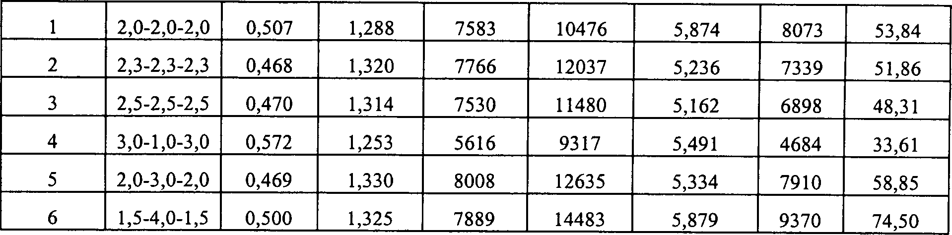
Die berechneten Spitzenzunahmen gp.max und die entsprechenden Wellenlängen λgp.max bei einer eingespritzen Trägerkonzentration von N = 1 × 1019 cm-3 (157 A/cm2) werden in Tabelle 1 für sechs Strukturen mit verschiedenen Senkenbreiten dA, dB, dA gezeigt. (I cl / hl)2 ist das Elektronen- und Lochwellenfunktionen überlappende Integral. Ne und Je sind sind die transparente Trägerkonzentration bzw. die transparente Stromdichte. gwn und gw sind Konstanten, die durch Anpassung der berechneten Verstärkungsspektren erhalten werden. Bei diesen hohen Einspritzpegeln wurde berechnet, dass die Lebensdauer der spontanen strahlenden Rekombination τsp ≈ 2,5 ns beträgt, und der Koeffizient der spontanen strahlenden Rekombination ist bei diesen Strukturen Bsp ≈ 4 × 10-11. Bei Struktur 5 wurde berechnet, dass die Transparenzträgerkonzentration ungefähr 5,3 × 1018 cm-3 (59 A/cm2) beträgt. Der Höchstwert des Verstärkungsspitzenwerts beträgt bei einer Trägereinspritzung von 1019 cm-3 8008 cm-1 und tritt bei einer Wellenlänge von 1,33 μm auf. Diese Trägerkonzentration ist für den Betrieb von VCSELs nicht unangemessen.The calculated peak magnitudes g p.max and the corresponding wavelengths λ gp.max at an injected carrier concentration of N = 1 × 10 19 cm -3 (157 A / cm 2 ) are given in Table 1 for six structures with different well widths d A , d B , d A shown. (I cl / hl) 2 is the electron and hole wave functions overlapping integral. N e and J e are the transparent carrier concentration and the transparent current density. g wn and g w are constants obtained by fitting the calculated gain spectra. At these high injection levels, it has been calculated that the lifetime of spontaneous radiative recombination is τ sp ≈ 2.5 ns, and the coefficient of spontaneous radiative recombination in these structures is Bsp ≈ 4 × 10 -11 . In structure 5, it was calculated that the transparency carrier concentration is about 5.3 × 10 18 cm -3 (59 A / cm 2 ). The peak value of the gain peak is 8008 cm -1 at a carrier injection of 10 19 cm -3 and occurs at a wavelength of 1.33 μm. This carrier concentration is not inappropriate for the operation of VCSELs.

Testproben und Bauelemente wurden bei einer Wachstumstemperatur von 505°C durch Molekularstrahl-Epitaxie (MBE) auf GaAs-Substraten gezüchtet. Die Proben für PL-Messungen wurden auf einem 20-Perioden-AlAs-GaAs-Supragitter, gefolgt von einer 220 nm-GaAs-Pufferschicht, gezüchtet, und sie wurden mit einer 10 nm dicken GaAs-Schicht abgedeckt. Die Nenndicke jeder Schicht betrug ungefähr 25-30 nm, abhängig von der Schichtzusammensetzung und folglich der Schichtbelastung, so dass die kritische Dicke nicht überschritten würde. Die In-Zielzusammensetzung wurde auf zwischen etwa 0,3 und 0,4 festgesetzt.test samples and devices were grown at a growth temperature of 505 ° C by molecular beam epitaxy (MBE) grown on GaAs substrates. The samples for PL measurements were made on a 20-period AlAs-GaAs supragitter, followed by a 220 nm-GaAs buffer layer, grown, and they were covered with a 10 nm thick GaAs layer. The Nominal thickness of each layer was about 25-30 nm, depending on the layer composition and thus the layer load, so that the critical thickness is not exceeded would. The in-target composition was set at between about 0.3 and 0.4.
Aufgrund der äußerst empfindlichen Abhängigkeit von Wachstumsparametern sind die absoluten Zusammensetzungen der Gruppe V (As, P, Sb) derzeit schwer aus Versuchen abzuleiten. Jener Ansatz, der zur Erzielung einer möglichen, bei 1,3 μm emtittierenden Struktur angewandt wird, ist wie folgt. Anfänglich wird bei 505°C eine Schichtsequenz von InxGa1-xAs/GaAs/InxGa1-xAs, gefolgt von GaAs, auf einem GaAs-Substrat gezüchtet. Jede der drei Schichten ist ungefähr 3 nm dick. Der In-Gehalt x wird solcherart angepasst, dass beide InxGa1-xAs-Schichten entweder gerade noch den Stranski-Krastanov-Aufrauhungsübergang erreichen oder gerade noch darunter bleiben. Es zeigt sich, dass beide Konfigurationen ungefähr bei derselben Wellenlänge emittieren. Im nächsten Schritt wird während des Wachstums der Mittelschicht der Sb-Fluss hinzugefügt, und der As-Fluss wird bei einem kostanten Gruppe-V-Fluss reduziert, was zu einer InxGa1-xAs/GaAssSb1-s/InxGa1-aAs-Struktur führt. Dieses Fließverhältnis wird in weiteren Wachstumsversuchen auf den höchstmöglichen Wert des Sb-Flusses angepasst, ohne erhebliche Versetzungsdichten einzubringen (gemessen durch eine Abnahme der PL-Intensität der resultierenden Struktur). Bei den folgenden Wachstumsvorgängen wird P eingebracht, bis die größtmögliche Wellenlänge erzielt wird.Due to the extremely sensitive dependence on growth parameters, the absolute group V compounds (As, P, Sb) are currently difficult to derive from experiments. The approach used to achieve a possible 1.3 μm emitter structure is as follows. Initially, at 505 ° C, a layer sequence of In x Ga 1-x As / GaAs / In x Ga 1-x As, followed by GaAs, is grown on a GaAs substrate. Each of the three layers is about 3 nm thick. The In content x is adjusted in such a way that both In x Ga 1-x As layers either just reach the Stranski-Krastanov roughening transition or just remain below it. It turns out that both configurations emit at approximately the same wavelength. In the next step, during the growth of the middle layer, the Sb flow is added and the As flow is reduced at a costly group V flow, resulting in an In x Ga 1-x As / GaAs s Sb 1-s / In x Ga 1-a As structure leads. This flow ratio is adjusted in further growth experiments to the highest possible value of the Sb flow, without introducing significant dislocation densities (measured by a decrease in the PL intensity of the resulting structure). In the following growth processes, P is introduced until the largest possible wavelength is achieved.
Die
Flüsse
der Gruppe-V-Elemente während
des Wachstums der zentralen GaPrAssSb1-r-s-Schicht
sind proportional zu den Ventileinstellungen der Elementarversorgungsquellen.
Die Zunahme eines Flussbestandteils führt auch zu einer Zunahme dieses
Bestandteils im festen Kristall, der sich entwickelt hat. Die Abhängigkeit
der PL-Emissionswellenlänge
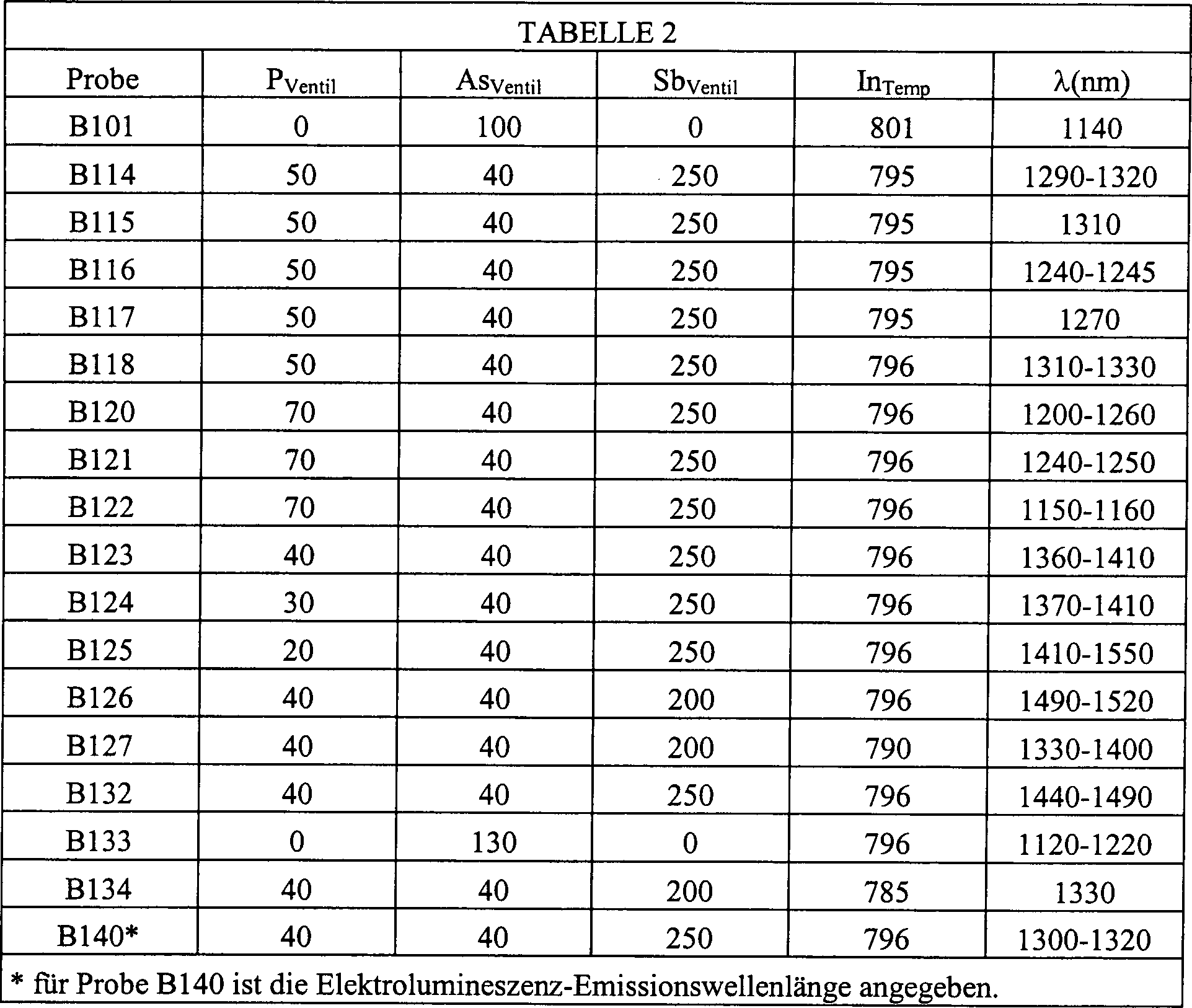
von den Ventileinstellungen der P-, As- und Sb-Quelle wird in Tabelle
2 und
Für die gezüchteten
Proben wird in
Obwohl
bei den relativen Veränderungen
der unterschiedlichen Zusammensetzungen zu beobachten ist, dass
sie auf die Emissionswellenlänge
eine reproduzierbare Wirkung ausüben,
wird die Zusammensetzung der Schichten dieser Ausführungsform
derzeit nur implizit durch den Wachstumsvorgang definiert. Sekundäre Ionenmasse-Spektroskopie (SIMS)-Messungen
einer Probe derselben, bei 1,3 μm
emittierenden Ausführungsform
werden in
Eine Verallgemeinerung aus diesen Versuchen und Berechnungen liefert die folgenden bevorzugten Zusammensetzungsbereiche der Schichtelemente. Bei der A-Schicht liegt x zwischen 0,05 und 0,7, y zwischen 0 und 0,35, z zwischen 0,45 und 1, und 1-y-z zwischen 0 und 0,25. Bei der B-Schicht liegt q zwischen 0 und 0,25 und 1-r-s zwischen 0,25 und 1. Unter Anwendung theoretischer Berechnungen werden Zusammensetzungsbereiche gewählt. Die Eingabedaten umfassen veröffentlichte Daten für Bandabstände und die Bandversetzung. Die Belastung wird ebenfalls berücksichtigt. Berechnungen für verschiedene Zusammensetzungen und Dicken sind obenstehend beschrieben. Die Zusammensetzungen werden mit einer maximalen Druckbelastung von etwa 4% berechnet, um das Wachstum dünner Schichten für deren versuchsweise Erzielung praktisch zu machen. Die Dicken werden dahingehend gewählt, dass das Material pseudomorph ist, egal welcher Belastung es unterliegt. Außerdem werden die Einschätzungen der SIMS-Daten verwendet. Die Daten für die Berechnungen und die Berechnungen selbst sind weithin bekannt.A generalization from these experiments and calculations provides the following preferred compositional ranges of the layer elements. In the A layer, x is between 0.05 and 0.7, y between 0 and 0.35, z between 0.45 and 1, and 1-yz between 0 and 0.25. For the B layer, q is between 0 and 0.25 and 1-rs between 0.25 and 1. Using theoretical calculations, composition ranges are chosen. The input data includes published data for band gaps and band offset. The load is also taken into account. Calculations for various compositions and thicknesses are described above. The compositions are calculated at a maximum compressive loading of about 4% to make the growth of thin films practical for their experimental use. The thicknesses are chosen so that the material is pseudomorphic, whichever Burden it is subject. In addition, the estimates of the SIMS data are used. The data for the calculations and the calculations themselves are well known.
Elektrisch
gepumpte, flankenemittierende Diodenproben wurden ebenfalls gezüchtet. Eine
schematische Struktur eines solchen Bauelements
Der
aktive Bereich
An
Proben wurden Raumtemperatur-PL-Messungen durchgeführt, wobei
für die
optische Anregung die 514 nm-Linie eines Argon-Ionenlasers verwendet
wurde. Dieses auf der epitaktisch gewachsenen Oberfläche der
Proben einfallende Licht wird vom Halbleitermaterial absorbiert,
und danach tritt eine Emission auf, wobei die optisch angeregten
Elektronen auf das Valenzband zurückfallen und sich mit Löchern rekombinieren, um
die Emission von Licht mit einer charakteristischen Wellenlänge, die
durch die Bandabstandseigenschaften des aktiven Material bestimmt
wurde, zu bewirken.
Reflection
High Energie Electron Diffraction (RHEED)-Messungen während des
Wachstums der Strukturen weisen auf eine andere Oberflächenanordnung
während
des Wachstums der mittleren (In)GaPAsSb („B")-Schicht hin. Dies ist in
Transmissions-Elektronenmikroskopie-Beobachtungen
von Querschnittsproben wurden durchgeführt, um die Schichtstruktur
von Proben zu kennzeichnen.
Die
vorliegende Erfindung kann in einer Reihe von verschiedenen optoelektronischen
Bauelementen eingebaut werden. Mehrere Variationen des flankenemittierenden
Bauelements
Die
Bauelemente
Die
vorliegende Erfindung kann in Resonanzhohlraumstrukturen, wie z.B.
Resonanzhohlraum-Photodioden (RCPD), Resonanzhohlraum-LEDs (RCLED)
oder VCSELs eingebaut werden. Ein Schema einer generischen Resonanzhohlraumstruktur
wird in
Haben sie sich auf GaAs-Strukturen entwickelt, so können die Spiegel aus dielektrischem Material mit hoher und niedriger Brechzahl, wie z.B. TiO2 bzw. SiO2, gebildet sein, die nur für das Beispiel verwendet werden. Es existieren auch noch andere gut bekannte dielektrische Materialien. Das Material mit hoher und niedriger Brechzahl kann der pseudomorphe Halbleiter AlxGa1-xAs bzw. AlyGa1-yAs sein, wobei y > x. Bei Halbleitern kann das Material mit niedrigerer Brechzahl auch oxidiertes AlyGa1-yAs sein, wobei y üblicherweise größer als 0,9 ist und x so gewählt ist, dass das Material nicht oxidiert. Ein Polymermaterial mit hoher und niedriger Brechzahl kann ebenfalls verwendet werden. Kombinationen aus jeglichen der obenstehenden Materialien mit niedriger und hoher Brechzahl können ebenso verwendet werden.Once developed on GaAs structures, the mirrors may be formed of high and low refractive index dielectric material such as TiO 2 and SiO 2, respectively, which are used only for the example. There are also other well-known dielectric materials. The high and low refractive index material may be the pseudomorphic semiconductor Al x Ga 1-x As and Al y Ga 1-y As, respectively, where y> x. For semiconductors, the lower refractive index material may also be oxidized Al y Ga 1-y As, where y is usually greater than 0.9 and x is selected so that the material does not oxidize. A high and low refractive index polymer material may also be used. Combinations of any of the above low and high refractive index materials may also be used.
Die Dicke der Spiegelschichten wird üblicherweise so gewählt, um λ/4 zu betragen. Dies definiert eine Hohlraumresonanz bei einer Wellenlänge von λ (in μm), welche als 1,24, geteilt durch die Resonanzenergie (in eV), definiert ist. Die Resonanzenergie sollte in das Verstärkungsspektrum des Materials des aktiven Bereichs fallen. Sie sollte so gewählt sein, um in der Nähe der Übergangsenergie des aktiven Bereichs zu liegen.The Thickness of the mirror layers usually becomes chosen so by λ / 4 too be. This defines a cavity resonance at a wavelength of λ (in μm), which is defined as 1.24, divided by the resonance energy (in eV). The resonance energy should be in the gain spectrum of the material of the active area. It should be chosen to be near the transition energy of the active area.
Bei
diesen Resonanzhohlraumstrukturen können über dem aktiven Bereich angeordnete Öffnungen verwendet
werden, um den optischen Modus zu leiten. Die Öffnungen haben vorzugsweise
zwei Bereiche.
Eine
zweite Art eines Bauelements mit Öffnung, eine brechzahlgeleitete Öffnung,
wird in
Eine
dritte Art eines Bauelements mit Öffnung, eine auf Oxid basierende
oder auf Oxid beschränkte Öffnung,
wird in
Die hier beschriebene Erfindung umfasst einen über einem Halbleitersubstrat angeordneten aktiven Bereich. Der aktive Bereich umfasst umfasst zumindest zwei pseudomorphe Schichten, welche die Form InxGa1-xPyAszSb1-y-z/InqGa1-qPrAssSb1-r-s aufweisen. Es zeigte sich, dass Strukturen, die diesen aktiven Bereich eingebaut haben, bei Wellenlängen von 1,1 μm bis mehr als 1,5 μm emittieren, welche für zahlreiche Anwendungen in der Telekommunikation geeignet sind. Das Züchten von InxGa1-xPyAszSb1-y-z/InqGa1-qPrAssSb1-r-s-Potentialtöpfen (QWs), wobei die Stöchiometrie der Schichten verschieden ist, auf GaAs- oder AlGaAs-Substraten verhindert die Einschränkung, dass die Laserwellenlänge durch den Bandabstand eines einzigen Materials bestimmt wird. Die Erfindung verschiebt die Spitze des Photolumineszenz (PL)-Emissionsspektrums von 1,1 μm auf 1,5 μm, abhängig von den Zusammensetzungen der InxGa1-xPyAszSb1-y-z und InqGa1-qPrAssSb1-r-s-Schichten. Ein theoretisches Formen zeigt, dass die vorgeschlagene QW- Struktur eine Bandkantenausrichtung des Typs II aufweist, wobei die Elektronen- und Lochwellenfunktionen eine große räumliche Überlappung aufweisen.The invention described herein includes an active region disposed over a semiconductor substrate. The active region comprises at least two pseudomorphic layers which have the form In x Ga 1 -x P y As z Sb 1-yz / In q Ga 1-q P r As s Sb 1-rs . It has been shown that structures incorporating this active region emit at wavelengths of 1.1 μm to more than 1.5 μm, which are suitable for numerous applications in telecommunications. Growing In x Ga 1 -x P y As z Sb 1-yz / In q Ga 1-q P r As s Sb 1-rs potential wells (QWs), where the stoichiometry of the layers is different, on GaAs or AlGaAs substrates prevent the limitation that the laser wavelength is determined by the bandgap of a single material. The invention shifts the peak of the photoluminescence (PL) emission spectrum of 1.1 μm to 1.5 μm, depending on the compositions of the In x Ga 1 -x P y As z Sb 1-yz and In q Ga 1-q P r As s Sb 1-rs layers. Theoretical shaping shows that the proposed QW structure has a Type II band edge orientation, where the electron and hole wave functions have a large spatial overlap.
Obwohl die vorliegende Erfindung im Detail beschrieben wurde, sollte verstanden werden, dass verschiedene Veränderungen, Austauschvorgänge und Abänderungen an ihr durchgeführt werden können, ohne vom durch die angeschlossenen Ansprüche definierten Umfang der Erfindung abzuweichen.Even though The present invention has been described in detail should be understood be that different changes, exchanges and amendments performed on her can be without the scope defined by the attached claims Deviate from the invention.
Claims (42)
Applications Claiming Priority (3)
| Application Number | Priority Date | Filing Date | Title |
|---|---|---|---|
| US11071898P | 1998-12-03 | 1998-12-03 | |
| US110718P | 1998-12-03 | ||
| PCT/US1999/028576 WO2000033433A2 (en) | 1998-12-03 | 1999-12-03 | Compound semiconductor structures for optoelectronic devices |
Publications (2)
| Publication Number | Publication Date |
|---|---|
| DE69921189D1 DE69921189D1 (en) | 2004-11-18 |
| DE69921189T2 true DE69921189T2 (en) | 2006-02-02 |
Family
ID=22334541
Family Applications (1)
| Application Number | Title | Priority Date | Filing Date |
|---|---|---|---|
| DE69921189T Expired - Fee Related DE69921189T2 (en) | 1998-12-03 | 1999-12-03 | CONNECTING SEMICONDUCTOR STRUCTURE FOR OPTOELECTRONIC COMPONENTS |
Country Status (7)
| Country | Link |
|---|---|
| US (1) | US6566688B1 (en) |
| EP (1) | EP1145395B1 (en) |
| JP (1) | JP2002531959A (en) |
| KR (1) | KR20010089540A (en) |
| AT (1) | ATE279799T1 (en) |
| DE (1) | DE69921189T2 (en) |
| WO (1) | WO2000033433A2 (en) |
Families Citing this family (36)
| Publication number | Priority date | Publication date | Assignee | Title |
|---|---|---|---|---|
| US6922426B2 (en) | 2001-12-20 | 2005-07-26 | Finisar Corporation | Vertical cavity surface emitting laser including indium in the active region |
| US7095770B2 (en) | 2001-12-20 | 2006-08-22 | Finisar Corporation | Vertical cavity surface emitting laser including indium, antimony and nitrogen in the active region |
| US7408964B2 (en) | 2001-12-20 | 2008-08-05 | Finisar Corporation | Vertical cavity surface emitting laser including indium and nitrogen in the active region |
| US7058112B2 (en) | 2001-12-27 | 2006-06-06 | Finisar Corporation | Indium free vertical cavity surface emitting laser |
| US6975660B2 (en) | 2001-12-27 | 2005-12-13 | Finisar Corporation | Vertical cavity surface emitting laser including indium and antimony in the active region |
| JP3735047B2 (en) * | 2000-07-31 | 2006-01-11 | 古河電気工業株式会社 | Semiconductor laser device and manufacturing method thereof |
| US6898224B2 (en) * | 2001-08-22 | 2005-05-24 | The Furukawa Electric Co., Ltd. | Semiconductor laser device |
| US6822995B2 (en) | 2002-02-21 | 2004-11-23 | Finisar Corporation | GaAs/AI(Ga)As distributed bragg reflector on InP |
| US7295586B2 (en) * | 2002-02-21 | 2007-11-13 | Finisar Corporation | Carbon doped GaAsSb suitable for use in tunnel junctions of long-wavelength VCSELs |
| KR100582540B1 (en) * | 2003-05-01 | 2006-05-23 | 한국전자통신연구원 | Formation of high quality quantum dots by using a strained layer |
| US7307375B2 (en) * | 2004-07-09 | 2007-12-11 | Energetiq Technology Inc. | Inductively-driven plasma light source |
| CA2581614A1 (en) | 2004-10-01 | 2006-04-13 | Finisar Corporation | Vertical cavity surface emitting laser having multiple top-side contacts |
| US7860137B2 (en) | 2004-10-01 | 2010-12-28 | Finisar Corporation | Vertical cavity surface emitting laser with undoped top mirror |
| WO2006072149A1 (en) * | 2005-01-07 | 2006-07-13 | Vrije Univeriteit Brussel | Broad-area microlasers and methods for driving them |
| US7952110B2 (en) * | 2006-06-12 | 2011-05-31 | 3M Innovative Properties Company | LED device with re-emitting semiconductor construction and converging optical element |
| US20070284565A1 (en) * | 2006-06-12 | 2007-12-13 | 3M Innovative Properties Company | Led device with re-emitting semiconductor construction and optical element |
| CN101467271B (en) * | 2006-06-12 | 2012-04-25 | 3M创新有限公司 | Led device with re-emitting semiconductor construction and converging optical element |
| US7902542B2 (en) * | 2006-06-14 | 2011-03-08 | 3M Innovative Properties Company | Adapted LED device with re-emitting semiconductor construction |
| JP2010034506A (en) * | 2008-06-24 | 2010-02-12 | Ricoh Co Ltd | Surface emission type semiconductor laser, surface emission type laser array element, optical scanning device, and image forming device |
| EP2131458B1 (en) * | 2008-06-03 | 2017-08-16 | Ricoh Company, Ltd. | Vertical cavity surface emitting laser (VCSEL), VCSEL array device, optical scanning apparatus, and image forming apparatus |
| WO2010121057A1 (en) * | 2009-04-16 | 2010-10-21 | Alliance For Sustainable Energy, Llc | LATTICE-MISMATCHED GaInP LED DEVICES AND METHODS OF FABRICATING SAME |
| TWI649895B (en) | 2010-04-30 | 2019-02-01 | 美國波士頓大學信託會 | High-efficiency ultraviolet light-emitting diode with variable structure position |
| WO2012051324A1 (en) | 2010-10-12 | 2012-04-19 | Alliance For Sustainable Energy, Llc | High bandgap iii-v alloys for high efficiency optoelectronics |
| DE102011103143B4 (en) * | 2011-05-25 | 2014-05-22 | Julius-Maximilians-Universität Würzburg | Interband cascade laser gain medium |
| JP2013004903A (en) * | 2011-06-21 | 2013-01-07 | Canon Inc | Semiconductor optical integrated element and optical tomograph equipped with the same |
| US8723189B1 (en) | 2012-01-06 | 2014-05-13 | Trustees Of Boston University | Ultraviolet light emitting diode structures and methods of manufacturing the same |
| JP2015008271A (en) * | 2013-05-31 | 2015-01-15 | 株式会社リコー | Surface emitting laser element and atomic oscillator |
| GB201501342D0 (en) * | 2015-01-27 | 2015-03-11 | Univ Lancaster | Improvements relating to the authentication of physical entities |
| JP7157162B2 (en) | 2017-09-18 | 2022-10-19 | タンペレ ユニバーシティ ファンデーション エスアール. | semiconductor multilayer structure |
| US20210218230A1 (en) * | 2018-05-24 | 2021-07-15 | The Regents Of The University Of California | Quantum dot lasers and methods for making the same |
| CN114223064A (en) * | 2019-02-18 | 2022-03-22 | 埃因霍芬理工大学 | Light-emitting or light-absorbing elements |
| US11862935B2 (en) * | 2019-05-30 | 2024-01-02 | Nippon Telegraph And Telephone Corporation | Tunable DBR semiconductor laser |
| US11804525B2 (en) * | 2019-10-11 | 2023-10-31 | The Regents Of The University Of California | Dislocation glide suppression for misfit dislocation free heteroepitaxy |
| JP7448994B2 (en) * | 2019-10-23 | 2024-03-13 | ザ リージェンツ オブ ザ ユニバーシティ オブ カリフォルニア | A method for fabricating resonant cavities and distributed Bragg reflector mirrors on wings of epitaxial lateral overgrowth regions for vertical cavity surface emitting lasers. |
| US11876350B2 (en) | 2020-11-13 | 2024-01-16 | Ii-Vi Delaware, Inc. | Multi-wavelength VCSEL array and method of fabrication |
| WO2023145148A1 (en) * | 2022-01-28 | 2023-08-03 | ソニーグループ株式会社 | Surface-emitting laser and method for manufacturing surface-emitting laser |
Family Cites Families (5)
| Publication number | Priority date | Publication date | Assignee | Title |
|---|---|---|---|---|
| US5767535A (en) * | 1994-03-25 | 1998-06-16 | Fraunhofer-Gesellschaft Zur Foerderung Der Angewandten Forschung E.V. | Quantum layer structure |
| JPH07335976A (en) | 1994-06-15 | 1995-12-22 | Nippon Telegr & Teleph Corp <Ntt> | Surface emission laser device with light receiving element |
| US5825796A (en) * | 1996-09-25 | 1998-10-20 | Picolight Incorporated | Extended wavelength strained layer lasers having strain compensated layers |
| US5719894A (en) | 1996-09-25 | 1998-02-17 | Picolight Incorporated | Extended wavelength strained layer lasers having nitrogen disposed therein |
| US5995529A (en) * | 1997-04-10 | 1999-11-30 | Sandia Corporation | Infrared light sources with semimetal electron injection |
-
1999
- 1999-12-03 DE DE69921189T patent/DE69921189T2/en not_active Expired - Fee Related
- 1999-12-03 US US09/856,799 patent/US6566688B1/en not_active Expired - Fee Related
- 1999-12-03 JP JP2000585975A patent/JP2002531959A/en not_active Withdrawn
- 1999-12-03 EP EP99967181A patent/EP1145395B1/en not_active Expired - Lifetime
- 1999-12-03 WO PCT/US1999/028576 patent/WO2000033433A2/en not_active Application Discontinuation
- 1999-12-03 AT AT99967181T patent/ATE279799T1/en not_active IP Right Cessation
- 1999-12-03 KR KR1020017006894A patent/KR20010089540A/en not_active Application Discontinuation
Also Published As
| Publication number | Publication date |
|---|---|
| DE69921189D1 (en) | 2004-11-18 |
| US6566688B1 (en) | 2003-05-20 |
| KR20010089540A (en) | 2001-10-06 |
| WO2000033433A2 (en) | 2000-06-08 |
| EP1145395B1 (en) | 2004-10-13 |
| ATE279799T1 (en) | 2004-10-15 |
| JP2002531959A (en) | 2002-09-24 |
| EP1145395A2 (en) | 2001-10-17 |
| WO2000033433A3 (en) | 2000-09-14 |
| WO2000033433B1 (en) | 2000-11-09 |
Similar Documents
| Publication | Publication Date | Title |
|---|---|---|
| DE69921189T2 (en) | CONNECTING SEMICONDUCTOR STRUCTURE FOR OPTOELECTRONIC COMPONENTS | |
| DE60225781T2 (en) | Long wavelength photonic device with InGaAsSb quantum well layer | |
| DE69636110T2 (en) | Semiconductor device with a miniband | |
| EP2191547B1 (en) | Optoelectronic component | |
| DE102009019996B4 (en) | DFB laser diode with lateral coupling for high output power | |
| DE60204007T2 (en) | SURFACE-EMITTING LASER WITH VERTICAL RESONATOR | |
| DE19756856B4 (en) | Semiconductor light emitting device with high light emission efficiency | |
| DE4434345A1 (en) | Cpd. semiconductor quantum well diode laser for operation at specific wavelength esp. 1.3 micron | |
| DE60107679T2 (en) | Indium phosphide-based vertical cavity surface emitting laser | |
| WO2011069769A2 (en) | Laser diode assembly and method for producing a laser diode assembly | |
| WO2008014772A1 (en) | Led semiconductor body | |
| DE60102343T2 (en) | Intersubband superlattice light-emitting device | |
| WO1999043056A1 (en) | Component with a light transmitter and a light receiver | |
| DE102008030818A1 (en) | Surface-emitting semiconductor laser with several active zones | |
| EP2191548B1 (en) | Radiation-emitting component | |
| DE10122063B4 (en) | Surface emitting semiconductor laser device | |
| EP2465148B1 (en) | Electrically pumped optoelectronic semiconductor chip | |
| DE10243545A1 (en) | Optically pumped semiconducting laser device has radiation emitting zone at first temperature, vertical emitter's radiation emitting zone at second, higher temperature when pump laser operating | |
| EP2255422B1 (en) | Infrared semiconductor laser | |
| DE10214568A1 (en) | Superficially radiating semiconductor laser component | |
| EP2109922B1 (en) | Unipolar, high efficiency quantum cascade laser | |
| WO2010048918A1 (en) | Optoelectronic semiconductor chip and method for producing an optoelectronic semiconductor chip | |
| WO2021214174A1 (en) | Semiconductor laser and lidar system and also laser system with the semiconductor laser | |
| WO2021239407A1 (en) | Semiconductor laser with a horizontal laser element and a vertical laser element, lidar system and production method | |
| EP2262067B1 (en) | Optoelectronic semiconductor element |
Legal Events
| Date | Code | Title | Description |
|---|---|---|---|
| 8364 | No opposition during term of opposition | ||
| 8339 | Ceased/non-payment of the annual fee |