DE112011102890T5 - Kesterite layer production for thin-film solar cells - Google Patents
Kesterite layer production for thin-film solar cells Download PDFInfo
- Publication number
- DE112011102890T5 DE112011102890T5 DE112011102890T DE112011102890T DE112011102890T5 DE 112011102890 T5 DE112011102890 T5 DE 112011102890T5 DE 112011102890 T DE112011102890 T DE 112011102890T DE 112011102890 T DE112011102890 T DE 112011102890T DE 112011102890 T5 DE112011102890 T5 DE 112011102890T5
- Authority
- DE
- Germany
- Prior art keywords
- substrate
- deposited
- sulfur
- substantially planar
- tin
- Prior art date
- Legal status (The legal status is an assumption and is not a legal conclusion. Google has not performed a legal analysis and makes no representation as to the accuracy of the status listed.)
- Ceased
Links
- 238000004519 manufacturing process Methods 0.000 title description 15
- 239000010409 thin film Substances 0.000 title description 11
- 239000000758 substrate Substances 0.000 claims abstract description 71
- 238000000137 annealing Methods 0.000 claims abstract description 34
- 238000000151 deposition Methods 0.000 claims abstract description 24
- 238000001704 evaporation Methods 0.000 claims abstract description 22
- 230000008020 evaporation Effects 0.000 claims abstract description 15
- 230000008021 deposition Effects 0.000 claims abstract description 14
- 238000000034 method Methods 0.000 claims description 85
- 239000006096 absorbing agent Substances 0.000 claims description 36
- 239000011669 selenium Substances 0.000 claims description 35
- 229910052717 sulfur Inorganic materials 0.000 claims description 34
- 230000008569 process Effects 0.000 claims description 28
- 229910052711 selenium Inorganic materials 0.000 claims description 28
- 239000011135 tin Substances 0.000 claims description 27
- 239000011701 zinc Substances 0.000 claims description 27
- NINIDFKCEFEMDL-UHFFFAOYSA-N Sulfur Chemical compound [S] NINIDFKCEFEMDL-UHFFFAOYSA-N 0.000 claims description 26
- 239000010949 copper Substances 0.000 claims description 26
- 239000011593 sulfur Substances 0.000 claims description 26
- 229910052718 tin Inorganic materials 0.000 claims description 26
- 229910052725 zinc Inorganic materials 0.000 claims description 25
- BUGBHKTXTAQXES-UHFFFAOYSA-N Selenium Chemical compound [Se] BUGBHKTXTAQXES-UHFFFAOYSA-N 0.000 claims description 24
- ATJFFYVFTNAWJD-UHFFFAOYSA-N Tin Chemical compound [Sn] ATJFFYVFTNAWJD-UHFFFAOYSA-N 0.000 claims description 23
- HCHKCACWOHOZIP-UHFFFAOYSA-N Zinc Chemical compound [Zn] HCHKCACWOHOZIP-UHFFFAOYSA-N 0.000 claims description 23
- 229910052802 copper Inorganic materials 0.000 claims description 23
- RYGMFSIKBFXOCR-UHFFFAOYSA-N Copper Chemical compound [Cu] RYGMFSIKBFXOCR-UHFFFAOYSA-N 0.000 claims description 21
- 239000000463 material Substances 0.000 claims description 19
- 238000004544 sputter deposition Methods 0.000 claims description 9
- ZOKXTWBITQBERF-UHFFFAOYSA-N Molybdenum Chemical compound [Mo] ZOKXTWBITQBERF-UHFFFAOYSA-N 0.000 claims description 8
- 229910052750 molybdenum Inorganic materials 0.000 claims description 8
- 239000011733 molybdenum Substances 0.000 claims description 8
- 238000005336 cracking Methods 0.000 claims description 7
- 238000001771 vacuum deposition Methods 0.000 claims description 7
- 238000000224 chemical solution deposition Methods 0.000 claims description 2
- 239000011248 coating agent Substances 0.000 claims 2
- 238000000576 coating method Methods 0.000 claims 2
- 239000011521 glass Substances 0.000 claims 2
- 238000005566 electron beam evaporation Methods 0.000 abstract description 5
- 229910052751 metal Inorganic materials 0.000 abstract description 5
- 239000002184 metal Substances 0.000 abstract description 5
- 238000005137 deposition process Methods 0.000 abstract description 2
- 238000001017 electron-beam sputter deposition Methods 0.000 abstract description 2
- 238000003860 storage Methods 0.000 description 19
- 238000012545 processing Methods 0.000 description 15
- 238000004590 computer program Methods 0.000 description 11
- 238000010586 diagram Methods 0.000 description 10
- 230000006870 function Effects 0.000 description 9
- 239000000203 mixture Substances 0.000 description 6
- GYHNNYVSQQEPJS-UHFFFAOYSA-N Gallium Chemical compound [Ga] GYHNNYVSQQEPJS-UHFFFAOYSA-N 0.000 description 5
- 238000012360 testing method Methods 0.000 description 5
- 229910052733 gallium Inorganic materials 0.000 description 4
- 229910052738 indium Inorganic materials 0.000 description 4
- APFVFJFRJDLVQX-UHFFFAOYSA-N indium atom Chemical compound [In] APFVFJFRJDLVQX-UHFFFAOYSA-N 0.000 description 4
- 238000002207 thermal evaporation Methods 0.000 description 4
- MARUHZGHZWCEQU-UHFFFAOYSA-N 5-phenyl-2h-tetrazole Chemical compound C1=CC=CC=C1C1=NNN=N1 MARUHZGHZWCEQU-UHFFFAOYSA-N 0.000 description 3
- 230000015572 biosynthetic process Effects 0.000 description 3
- 238000010438 heat treatment Methods 0.000 description 3
- 230000007246 mechanism Effects 0.000 description 3
- 239000005361 soda-lime glass Substances 0.000 description 3
- 241001136792 Alle Species 0.000 description 2
- XKRFYHLGVUSROY-UHFFFAOYSA-N Argon Chemical compound [Ar] XKRFYHLGVUSROY-UHFFFAOYSA-N 0.000 description 2
- IJGRMHOSHXDMSA-UHFFFAOYSA-N Atomic nitrogen Chemical compound N#N IJGRMHOSHXDMSA-UHFFFAOYSA-N 0.000 description 2
- OAKJQQAXSVQMHS-UHFFFAOYSA-N Hydrazine Chemical compound NN OAKJQQAXSVQMHS-UHFFFAOYSA-N 0.000 description 2
- 238000009713 electroplating Methods 0.000 description 2
- 230000008018 melting Effects 0.000 description 2
- 238000002844 melting Methods 0.000 description 2
- 238000012986 modification Methods 0.000 description 2
- 230000004048 modification Effects 0.000 description 2
- 230000003287 optical effect Effects 0.000 description 2
- 230000000644 propagated effect Effects 0.000 description 2
- 238000001228 spectrum Methods 0.000 description 2
- 231100000331 toxic Toxicity 0.000 description 2
- 230000002588 toxic effect Effects 0.000 description 2
- XLOMVQKBTHCTTD-UHFFFAOYSA-N zinc oxide Inorganic materials [Zn]=O XLOMVQKBTHCTTD-UHFFFAOYSA-N 0.000 description 2
- 239000011787 zinc oxide Substances 0.000 description 2
- 229910001128 Sn alloy Inorganic materials 0.000 description 1
- 229910001297 Zn alloy Inorganic materials 0.000 description 1
- 230000009471 action Effects 0.000 description 1
- 238000013459 approach Methods 0.000 description 1
- 229910052786 argon Inorganic materials 0.000 description 1
- 230000009286 beneficial effect Effects 0.000 description 1
- 229910052793 cadmium Inorganic materials 0.000 description 1
- BDOSMKKIYDKNTQ-UHFFFAOYSA-N cadmium atom Chemical compound [Cd] BDOSMKKIYDKNTQ-UHFFFAOYSA-N 0.000 description 1
- 238000010549 co-Evaporation Methods 0.000 description 1
- 239000004020 conductor Substances 0.000 description 1
- 238000001816 cooling Methods 0.000 description 1
- HVMJUDPAXRRVQO-UHFFFAOYSA-N copper indium Chemical compound [Cu].[In] HVMJUDPAXRRVQO-UHFFFAOYSA-N 0.000 description 1
- 238000004090 dissolution Methods 0.000 description 1
- 230000000694 effects Effects 0.000 description 1
- 239000002360 explosive Substances 0.000 description 1
- 239000000835 fiber Substances 0.000 description 1
- 239000010408 film Substances 0.000 description 1
- 239000007789 gas Substances 0.000 description 1
- 239000003365 glass fiber Substances 0.000 description 1
- AMGQUBHHOARCQH-UHFFFAOYSA-N indium;oxotin Chemical compound [In].[Sn]=O AMGQUBHHOARCQH-UHFFFAOYSA-N 0.000 description 1
- 239000011261 inert gas Substances 0.000 description 1
- 229910000464 lead oxide Inorganic materials 0.000 description 1
- 230000007774 longterm Effects 0.000 description 1
- 229910052757 nitrogen Inorganic materials 0.000 description 1
- YEXPOXQUZXUXJW-UHFFFAOYSA-N oxolead Chemical compound [Pb]=O YEXPOXQUZXUXJW-UHFFFAOYSA-N 0.000 description 1
- 230000001902 propagating effect Effects 0.000 description 1
- 230000000630 rising effect Effects 0.000 description 1
- SBIBMFFZSBJNJF-UHFFFAOYSA-N selenium;zinc Chemical compound [Se]=[Zn] SBIBMFFZSBJNJF-UHFFFAOYSA-N 0.000 description 1
- 150000003346 selenoethers Chemical class 0.000 description 1
- 239000004065 semiconductor Substances 0.000 description 1
- 238000000926 separation method Methods 0.000 description 1
- 239000007779 soft material Substances 0.000 description 1
- 239000007787 solid Substances 0.000 description 1
- 239000010935 stainless steel Substances 0.000 description 1
- 229910001220 stainless steel Inorganic materials 0.000 description 1
- 229910052714 tellurium Inorganic materials 0.000 description 1
- PORWMNRCUJJQNO-UHFFFAOYSA-N tellurium atom Chemical compound [Te] PORWMNRCUJJQNO-UHFFFAOYSA-N 0.000 description 1
- YVTHLONGBIQYBO-UHFFFAOYSA-N zinc indium(3+) oxygen(2-) Chemical compound [O--].[Zn++].[In+3] YVTHLONGBIQYBO-UHFFFAOYSA-N 0.000 description 1
Images


Classifications
-
- H—ELECTRICITY
- H01—ELECTRIC ELEMENTS
- H01L—SEMICONDUCTOR DEVICES NOT COVERED BY CLASS H10
- H01L31/00—Semiconductor devices sensitive to infrared radiation, light, electromagnetic radiation of shorter wavelength or corpuscular radiation and specially adapted either for the conversion of the energy of such radiation into electrical energy or for the control of electrical energy by such radiation; Processes or apparatus specially adapted for the manufacture or treatment thereof or of parts thereof; Details thereof
- H01L31/04—Semiconductor devices sensitive to infrared radiation, light, electromagnetic radiation of shorter wavelength or corpuscular radiation and specially adapted either for the conversion of the energy of such radiation into electrical energy or for the control of electrical energy by such radiation; Processes or apparatus specially adapted for the manufacture or treatment thereof or of parts thereof; Details thereof adapted as photovoltaic [PV] conversion devices
- H01L31/06—Semiconductor devices sensitive to infrared radiation, light, electromagnetic radiation of shorter wavelength or corpuscular radiation and specially adapted either for the conversion of the energy of such radiation into electrical energy or for the control of electrical energy by such radiation; Processes or apparatus specially adapted for the manufacture or treatment thereof or of parts thereof; Details thereof adapted as photovoltaic [PV] conversion devices characterised by at least one potential-jump barrier or surface barrier
- H01L31/072—Semiconductor devices sensitive to infrared radiation, light, electromagnetic radiation of shorter wavelength or corpuscular radiation and specially adapted either for the conversion of the energy of such radiation into electrical energy or for the control of electrical energy by such radiation; Processes or apparatus specially adapted for the manufacture or treatment thereof or of parts thereof; Details thereof adapted as photovoltaic [PV] conversion devices characterised by at least one potential-jump barrier or surface barrier the potential barriers being only of the PN heterojunction type
-
- H—ELECTRICITY
- H01—ELECTRIC ELEMENTS
- H01L—SEMICONDUCTOR DEVICES NOT COVERED BY CLASS H10
- H01L21/00—Processes or apparatus adapted for the manufacture or treatment of semiconductor or solid state devices or of parts thereof
- H01L21/02—Manufacture or treatment of semiconductor devices or of parts thereof
- H01L21/02104—Forming layers
- H01L21/02365—Forming inorganic semiconducting materials on a substrate
- H01L21/02367—Substrates
- H01L21/0237—Materials
- H01L21/02422—Non-crystalline insulating materials, e.g. glass, polymers
-
- H—ELECTRICITY
- H01—ELECTRIC ELEMENTS
- H01L—SEMICONDUCTOR DEVICES NOT COVERED BY CLASS H10
- H01L21/00—Processes or apparatus adapted for the manufacture or treatment of semiconductor or solid state devices or of parts thereof
- H01L21/02—Manufacture or treatment of semiconductor devices or of parts thereof
- H01L21/02104—Forming layers
- H01L21/02365—Forming inorganic semiconducting materials on a substrate
- H01L21/02436—Intermediate layers between substrates and deposited layers
- H01L21/02439—Materials
- H01L21/02485—Other chalcogenide semiconducting materials not being oxides, e.g. ternary compounds
-
- H—ELECTRICITY
- H01—ELECTRIC ELEMENTS
- H01L—SEMICONDUCTOR DEVICES NOT COVERED BY CLASS H10
- H01L21/00—Processes or apparatus adapted for the manufacture or treatment of semiconductor or solid state devices or of parts thereof
- H01L21/02—Manufacture or treatment of semiconductor devices or of parts thereof
- H01L21/02104—Forming layers
- H01L21/02365—Forming inorganic semiconducting materials on a substrate
- H01L21/02436—Intermediate layers between substrates and deposited layers
- H01L21/02439—Materials
- H01L21/02491—Conductive materials
-
- H—ELECTRICITY
- H01—ELECTRIC ELEMENTS
- H01L—SEMICONDUCTOR DEVICES NOT COVERED BY CLASS H10
- H01L21/00—Processes or apparatus adapted for the manufacture or treatment of semiconductor or solid state devices or of parts thereof
- H01L21/02—Manufacture or treatment of semiconductor devices or of parts thereof
- H01L21/02104—Forming layers
- H01L21/02365—Forming inorganic semiconducting materials on a substrate
- H01L21/02436—Intermediate layers between substrates and deposited layers
- H01L21/02494—Structure
- H01L21/02496—Layer structure
- H01L21/02502—Layer structure consisting of two layers
-
- H—ELECTRICITY
- H01—ELECTRIC ELEMENTS
- H01L—SEMICONDUCTOR DEVICES NOT COVERED BY CLASS H10
- H01L21/00—Processes or apparatus adapted for the manufacture or treatment of semiconductor or solid state devices or of parts thereof
- H01L21/02—Manufacture or treatment of semiconductor devices or of parts thereof
- H01L21/02104—Forming layers
- H01L21/02365—Forming inorganic semiconducting materials on a substrate
- H01L21/02518—Deposited layers
- H01L21/02521—Materials
- H01L21/02551—Group 12/16 materials
- H01L21/02557—Sulfides
-
- H—ELECTRICITY
- H01—ELECTRIC ELEMENTS
- H01L—SEMICONDUCTOR DEVICES NOT COVERED BY CLASS H10
- H01L21/00—Processes or apparatus adapted for the manufacture or treatment of semiconductor or solid state devices or of parts thereof
- H01L21/02—Manufacture or treatment of semiconductor devices or of parts thereof
- H01L21/02104—Forming layers
- H01L21/02365—Forming inorganic semiconducting materials on a substrate
- H01L21/02518—Deposited layers
- H01L21/02521—Materials
- H01L21/02568—Chalcogenide semiconducting materials not being oxides, e.g. ternary compounds
-
- H—ELECTRICITY
- H01—ELECTRIC ELEMENTS
- H01L—SEMICONDUCTOR DEVICES NOT COVERED BY CLASS H10
- H01L21/00—Processes or apparatus adapted for the manufacture or treatment of semiconductor or solid state devices or of parts thereof
- H01L21/02—Manufacture or treatment of semiconductor devices or of parts thereof
- H01L21/02104—Forming layers
- H01L21/02365—Forming inorganic semiconducting materials on a substrate
- H01L21/02612—Formation types
- H01L21/02617—Deposition types
- H01L21/02623—Liquid deposition
- H01L21/02628—Liquid deposition using solutions
-
- H—ELECTRICITY
- H01—ELECTRIC ELEMENTS
- H01L—SEMICONDUCTOR DEVICES NOT COVERED BY CLASS H10
- H01L21/00—Processes or apparatus adapted for the manufacture or treatment of semiconductor or solid state devices or of parts thereof
- H01L21/02—Manufacture or treatment of semiconductor devices or of parts thereof
- H01L21/02104—Forming layers
- H01L21/02365—Forming inorganic semiconducting materials on a substrate
- H01L21/02612—Formation types
- H01L21/02617—Deposition types
- H01L21/02631—Physical deposition at reduced pressure, e.g. MBE, sputtering, evaporation
-
- H—ELECTRICITY
- H01—ELECTRIC ELEMENTS
- H01L—SEMICONDUCTOR DEVICES NOT COVERED BY CLASS H10
- H01L31/00—Semiconductor devices sensitive to infrared radiation, light, electromagnetic radiation of shorter wavelength or corpuscular radiation and specially adapted either for the conversion of the energy of such radiation into electrical energy or for the control of electrical energy by such radiation; Processes or apparatus specially adapted for the manufacture or treatment thereof or of parts thereof; Details thereof
- H01L31/0248—Semiconductor devices sensitive to infrared radiation, light, electromagnetic radiation of shorter wavelength or corpuscular radiation and specially adapted either for the conversion of the energy of such radiation into electrical energy or for the control of electrical energy by such radiation; Processes or apparatus specially adapted for the manufacture or treatment thereof or of parts thereof; Details thereof characterised by their semiconductor bodies
- H01L31/0256—Semiconductor devices sensitive to infrared radiation, light, electromagnetic radiation of shorter wavelength or corpuscular radiation and specially adapted either for the conversion of the energy of such radiation into electrical energy or for the control of electrical energy by such radiation; Processes or apparatus specially adapted for the manufacture or treatment thereof or of parts thereof; Details thereof characterised by their semiconductor bodies characterised by the material
- H01L31/0264—Inorganic materials
- H01L31/032—Inorganic materials including, apart from doping materials or other impurities, only compounds not provided for in groups H01L31/0272 - H01L31/0312
- H01L31/0326—Inorganic materials including, apart from doping materials or other impurities, only compounds not provided for in groups H01L31/0272 - H01L31/0312 comprising AIBIICIVDVI kesterite compounds, e.g. Cu2ZnSnSe4, Cu2ZnSnS4
-
- Y—GENERAL TAGGING OF NEW TECHNOLOGICAL DEVELOPMENTS; GENERAL TAGGING OF CROSS-SECTIONAL TECHNOLOGIES SPANNING OVER SEVERAL SECTIONS OF THE IPC; TECHNICAL SUBJECTS COVERED BY FORMER USPC CROSS-REFERENCE ART COLLECTIONS [XRACs] AND DIGESTS
- Y02—TECHNOLOGIES OR APPLICATIONS FOR MITIGATION OR ADAPTATION AGAINST CLIMATE CHANGE
- Y02E—REDUCTION OF GREENHOUSE GAS [GHG] EMISSIONS, RELATED TO ENERGY GENERATION, TRANSMISSION OR DISTRIBUTION
- Y02E10/00—Energy generation through renewable energy sources
- Y02E10/50—Photovoltaic [PV] energy
Abstract
Eine Kesteritschicht wird auf ein Substrat vakuumabgeschieden und geglüht. Die Abscheidung wird bei einer niedrigen Temperatur durchgeführt, um eine gute Steuerung der Zusammensetzung und eine effiziente Metallausnutzung zu gewährleisten. Das Glühen wird eine kurze Zeit lang bei einer hohen Temperatur durchgeführt. Wärmeverdampfung, Elektronenstrahlverdampfung oder Zerstäubung können als Teil eines Abscheidungsprozesses in einer Hochvakuumumgebung verwendet werden.A kesterite layer is vacuum deposited on a substrate and annealed. The deposition is carried out at a low temperature to ensure good compositional control and efficient metal utilization. The annealing is carried out at a high temperature for a short time. Heat evaporation, electron beam evaporation or sputtering may be used as part of a deposition process in a high vacuum environment.
Description
Technisches GebietTechnical area
Die vorliegende Erfindung betrifft die physikalischen Wissenschaften und insbesondere Fertigungstechniken und dergleichen.The present invention relates to physical sciences, and more particularly to manufacturing techniques and the like.
Hintergrundbackground
Gegenwärtig sind Kupfer-Indium-Gallium-(Di)selenid, auch als Cu2InGa(S, Se)4 oder CIGS bekannt, und Cadmium-Tellurid (CdTe) die Hauptmaterialien, die zur Verwendung in Dünnschicht-Solarzellen entwickelt wurden. Was das CIGS-Material anbetrifft, sind die Preise für Indium und Gallium hoch. Aufgrund der zunehmenden Nachfrage nach Indium-Zink-Oxid (ITO) zur Verwendung in Flachbildschirmen sind die Preise für Indium in den letzten Jahren stetig gestiegen. Was CdTe anbetrifft, ist Cadmium toxisch und Tellur ziemlich selten. Absorbermaterialien, die Kupfer, Zink, Zinn und Schwefel und/oder Selen enthalten, bieten eine wirtschaftlichere Alternative, da sie an Stelle von Gallium und Indium, die im CIGS-Material zu finden sind, Kupfer und Zink verwenden, die relativ reichlich vorhanden sind.At present, copper indium gallium (di) selenide, also known as Cu2InGa (S, Se) 4 or CIGS, and cadmium telluride (CdTe) are the major materials developed for use in thin film solar cells. As far as the CIGS material is concerned, the prices of indium and gallium are high. Due to the increasing demand for indium zinc oxide (ITO) for use in flat panel displays, indium prices have been rising steadily in recent years. As for CdTe, cadmium is toxic and tellurium is quite rare. Absorber materials containing copper, zinc, tin, and sulfur and / or selenium offer a more economical alternative because they use copper and zinc, which are relatively abundant, rather than gallium and indium found in the CIGS material.
Kurzbeschreibung der ErfindungBrief description of the invention
Prinzipien der Erfindung stellen Techniken zur Bildung einer Absorberschicht auf ein Substrat bereit; zum Beispiel, um Cu2ZnSn(SxSe4-x)-Dünnschichten (”CZTSSe”) auf Substrate für Solarzellenanwendungen abzuscheiden, wobei x von null bis vier variiert. In einem Aspekt umfasst ein beispielhaftes Verfahren das Bereitstellen eines Substrats, das Aussetzen des Substrats einer Hochvakuumumgebung, das Abscheiden von Kupfer, Zink, Zinn und mindestens einem von Schwefel und Selen auf eine Oberfläche des Substrats durch Wärmeverdampfung, während die Temperatur des Substrats auf einen Bereich gehalten wird, der niedrig genug ist, damit ein Wiederverdampfen des auf dem Substrat abgeschiedenen Materials nicht wesentlich ist, wodurch eine Absorberschicht gebildet wird, die für Solarzellen-Anwendungen geeignet ist, und das Glühen der auf dem Substrat abgeschiedenen Absorberschicht bei einer zweiten Temperatur, die wesentlich höher ist als die Temperatur, die während des Abscheidungsschritts gehalten wird.Principles of the invention provide techniques for forming an absorber layer on a substrate; for example, to deposit Cu 2 ZnSn (S x Se 4-x ) thin films ("CZTSSe") on substrates for solar cell applications where x varies from zero to four. In one aspect, an exemplary method includes providing a substrate, exposing the substrate to a high vacuum environment, depositing copper, zinc, tin, and at least one of sulfur and selenium onto a surface of the substrate by thermal evaporation while the temperature of the substrate is within a range which is low enough so that re-evaporation of the material deposited on the substrate is not essential, thereby forming an absorber layer suitable for solar cell applications and annealing the absorber layer deposited on the substrate at a second temperature is much higher than the temperature held during the deposition step.
In einem weiteren Aspekt umfasst ein beispielhaftes Verfahren die Schritte des Bereitstellens eines Substrats mit einer im Wesentlichen planen Oberfläche, das Vakuumabscheiden von Kupfer, Zink, Zinn und mindestens einem von Schwefel und Selen auf der im Wesentlichen planen Oberfläche des Substrats, während die Temperatur des Substrats auf einen Bereich gehalten wird, der niedrig genug ist, damit ein Wiederverdampfen des auf dem Substrat abgeschiedenen Materials nicht wesentlich ist, wodurch eine Absorberschicht gebildet wird, die für Solarzellen-Anwendungen geeignet ist, das Glühen der auf dem Substrat vakuumabgeschiedenen Absorberschicht bei einer Temperatur über 300°C, das Bereitstellen einer Emitterschicht auf der Absorberschicht, und das Bereitstellen einer Fensterschicht über der Emitterschicht.In another aspect, an exemplary method includes the steps of providing a substrate having a substantially planar surface, vacuum depositing copper, zinc, tin, and at least one of sulfur and selenium on the substantially planar surface of the substrate while maintaining the temperature of the substrate is kept low enough so that re-evaporation of the deposited material on the substrate is not essential, thereby forming an absorber layer suitable for solar cell applications, annealing the absorber layer vacuum deposited on the substrate at a temperature above 300 ° C, providing an emitter layer on the absorber layer, and providing a window layer over the emitter layer.
In einem weiteren Aspekt der Erfindung umfasst ein beispielhaftes Verfahren das Bereitstellen eines Substrats mit einer im Wesentlichen planen Oberfläche; das Halten der Temperatur des Substrats zwischen 100 und 200°C; das Vakuumabscheiden von Cu, Zn, Sn und mindestens einem von S und Se auf der im Wesentlichen planen Oberfläche des Substrats, wodurch auf der im Wesentlichen planen Oberfläche eine Absorberschicht gebildet wird, die für Solarzellen-Anwendungen geeignet ist, und das Glühen der auf dem Substrat vakuumabgeschiedenen Absorberschicht bei einer Temperatur zwischen 300 und 600°C.In another aspect of the invention, an exemplary method includes providing a substrate having a substantially planar surface; maintaining the temperature of the substrate between 100 and 200 ° C; vacuum deposition of Cu, Zn, Sn and at least one of S and Se on the substantially planar surface of the substrate, thereby forming on the substantially planar surface an absorber layer suitable for solar cell applications and the annealing of the on the Substrate vacuum deposited absorber layer at a temperature between 300 and 600 ° C.
Hierin bedeutet das ”Erleichtern” eines Vorgangs, dass ein Vorgang durchgeführt, erleichtert, unterstützt oder veranlasst wird. So können, zum Beispiel und auf nicht einschränkende Weise, Anweisungen, die auf einem Prozessor ausgeführt werden, eine Aktion erleichtern, der von einer Herstellungs- oder Testausrüstung durchgeführt wird, oder auch Anweisungen, die auf einem entfernten Prozessor ausgeführt werden, indem geeignete Daten oder Befehle übertragen werden, um den durchzuführenden Vorgang zu veranlassen oder zu unterstützen. Um jeden Zweifel auszuschließen, wenn ein „Aktor” einen Vorgang auf andere Weise erleichtert, als indem er ihn durchführt, wird der Vorgang dennoch von derselben Entität oder Kombination von Entitäten durchgeführt.Herein, "facilitating" an operation means that an operation is performed, facilitated, assisted, or initiated. Thus, for example, and not by way of limitation, instructions that are executed on a processor may facilitate an action performed by a manufacturing or testing equipment, or instructions that are executed on a remote processor, by appropriate data or data Commands are transmitted to initiate or support the process to be performed. To eliminate any doubt, if an "actor" facilitates a process in ways other than performing it, the process is still performed by the same entity or combination of entities.
Eine oder mehrere Ausführungsformen der Erfindung oder Elemente davon (zum Beispiel die Computersteuerung eines Abscheidungs-, Glüh- oder zugehörigen Herstellungs- oder Testprozesses) können in Form eines Computerprodukts realisiert werden, das ein computerlesbares Speichermedium mit computernutzbarem Programmcode zur Durchführung der angegebenen Verfahrensschritte aufweist. Ferner können eine oder mehrere Ausführungsformen der Erfindung oder Elemente davon in Form eines Systems (oder einer Vorrichtung) realisiert werden, das (die) einen Speicher und mindestens einen Prozessor aufweist, der mit dem Speicher verbunden ist und betreibbar ist, um beispielhafte Verfahrensschritte durchzuführen. In einem weiteren Aspekt können eine oder mehrere Ausführungsformen der Erfindung oder Elemente davon in Form von Mitteln zur Durchführung eines oder mehrerer der hierin beschriebenen Verfahrensschritte realisiert werden; die Mittel können (i) Hardware-Modul(e), (ii) Software-Modul(e) oder (iii) eine Kombination aus Hardware- und Software-Modulen aufweisen, jedes von (i) bis (iii) realisiert die spezifischen Techniken, die hierin dargelegt werden, und die Software-Module werden auf einem computerlesbaren Speichermedium (oder mehreren solcher Medien) gespeichert.One or more embodiments of the invention or elements thereof (eg, computer control of a deposition, annealing, or associated manufacturing or testing process) may be implemented in the form of a computer product having a computer readable storage medium with computer usable program code for performing the specified method steps. Furthermore, one or more embodiments of the invention or elements thereof may be implemented in the form of a system (or device) having a memory and at least one processor connected to the memory and operable to perform example method steps. In another aspect, one or more embodiments of the invention, or elements thereof, may be practiced as means for performing one or more of the method steps described herein; the means may be (i) hardware module (s), (ii) Software module (s) or (iii) comprise a combination of hardware and software modules, each of (i) to (iii) implements the specific techniques set forth herein and the software modules are stored on a computer readable storage medium (or more of such media).
Techniken der vorliegenden Erfindung können wesentliche vorteilhafte technische Wirkungen aufweisen. Zum Beispiel können eine oder mehrere Ausführungsformen einen oder mehrere der folgenden Vorteile bieten:
- • der Fluss jedes Elements kann während der Vakuumabscheidung einzeln gesteuert werden, um eine präzise Zusammensetzung zu erreichen;
- • das Substrat kann während der Abscheidung erwärmt werden;
- • alle Elemente, aus denen das Kesteritmaterial besteht, können gleichzeitig abgeschieden werden;
- • die verwendeten Verfahren sind alle umweltsicher.
- The flow of each element can be individually controlled during vacuum deposition to achieve precise composition;
- The substrate can be heated during the deposition;
- • all elements that make up the kesterite material can be deposited simultaneously;
- • the procedures used are all environmentally safe.
Kurze Beschreibung der ZeichnungenBrief description of the drawings
Ausführungsformen der Erfindung werden nun lediglich beispielhaft Bezug nehmend auf die beiliegenden Zeichnungen beschrieben, wobei:Embodiments of the invention will now be described, by way of example only, with reference to the accompanying drawings, in which:
Ausführliche BeschreibungDetailed description
Kesterit, auch als Cu2ZnSnSxSe4-x oder CZTSSe bekannt, verspricht kostengünstige, erneuerbare Solarzellen, da alle verwendeten Elemente billig und auf der Erde reichlich vorhanden sind. Im Gegensatz zu CIGS-Absorbern, die die relativ teuren Elemente Indium und Gallium erfordern, sind Zink und Zinn zu vertretbaren Preisen leicht verfügbar, und Kesterit-Dünnschichten wurden durch verschiedene Techniken einschließlich Wärmeverdampfung, Lösungsprozesse, Elektroplattierung, Zerstäubung und dergleichen abgeschieden. Lösungsprozesse können Hydrazin erfordern, das sowohl explosiv als auch toxisch ist. Zerstäubungstechniken und Elektroplattierung beinhalten typischerweise die Abscheidung einer Cu/Zn/Sn-Legierung, gefolgt von einem mehr als zwei Stunden langen Glühen mit H2S oder S.Kesterite, also known as Cu 2 ZnSnS x Se 4-x or CZTSSe, promises low-cost, renewable solar cells because all the elements used are cheap and abundant on Earth. In contrast to CIGS absorbers, which require the relatively expensive elements indium and gallium, zinc and tin are readily available at reasonable prices, and kesterite films have been deposited by various techniques including heat evaporation, dissolution processes, electroplating, sputtering, and the like. Solution processes may require hydrazine, which is both explosive and toxic. Sputtering techniques and electroplating typically involve the deposition of a Cu / Zn / Sn alloy, followed by annealing with H 2 S or S for more than two hours.
Die meisten Fertigungsabläufe erfordern ein Hochtemperaturglühen (> 500°C), um große Körner für die Kesterit-Absorberschicht wachsen zu lassen. Gängige Verfahren, die für das Hochtemperaturglühen verwendet werden, schließen das Glühen in einem Ofen mit strömendem H2S-Gas und das Glühen im Inneren eines geschlossenen Rohrs mit ausreichendem S-Dampfdruck ein. Solche Verfahren können Probleme mit einem oder mehreren von der Temperaturgleichmäßigkeit, dem Verlust von Sn, S und/oder Se bei hoher Temperatur, der Oberflächenebenheit und der Korngrößenregelung mit sich bringen. Überdies erfordern sie typischerweise eine lange Zeit für den Glühprozess, z. B. 1 bis 3 Stunden bei Glühtemperatur mit zusätzlich 1 bis 3 Stunden Abkühlzeit. An Stelle des Hochtemperaturglühens besteht ein anderer Ansatz darin, Materialien bei hoher Substrattemperatur (> 400°C) abzuscheiden. Dieses Verfahren erfordert kein Langzeitglühen, doch der Sn/Zn-Verlust ist signifikant und die Materialausnutzung unzureichend. Eine oder mehrere Ausführungsformen der Erfindung benötigen nur fünf (5) bis zwanzig (20) Minuten Glühzeit mit einer Wärmeplatte. Eine geschlossene H2S-Kammer ist nicht erforderlich.Most manufacturing processes require high temperature annealing (> 500 ° C) to grow large grains for the kesterite absorber layer. Common methods used for high temperature annealing include annealing in an oven with flowing H 2 S gas and annealing inside a closed tube with sufficient S vapor pressure. Such methods may involve problems with one or more of temperature uniformity, loss of Sn, S, and / or Se at high temperature, surface flatness, and grain size control. Moreover, they typically require a long time for the annealing process, e.g. B. 1 to 3 hours at annealing temperature with an additional 1 to 3 hours cooling time. Instead of high-temperature annealing, another approach is to deposit materials at high substrate temperature (> 400 ° C). This method does not require long term annealing, but the Sn / Zn loss is significant and the material utilization is insufficient. One or more embodiments of the invention require only five (5) to twenty (20) minutes of annealing time with a hot plate. A closed H 2 S chamber is not required.
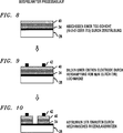
Wärmeverdampfung ist eine Technik, die allgemein das Erwärmen einer festen Quelle beinhaltet, um Atome oder Cluster aus Atomen zu erzeugen, die unter Hochvakuumbedingungen zu einem erwärmten Substrat migrieren. Die Atome diffundieren auf der Substratoberfläche und bilden darauf eine Dünnschicht. Systeme zur Durchführung der Wärmeverdampfung weisen gewöhnlich Effusionszellen auf, die auf den Substratheizer fokussiert sind. Die Effusionszellen enthalten die Elemente, die zur Bildung der Dünnschicht verwendet werden. Ein Mechanismus zum Drehen des Substrats kann vorgesehen sein, um die Gleichmäßigkeit der Dünnschichtbildung zu erhöhen. Systeme, die Abscheidungstechniken durch Wärmeverdampfung verwenden, sind dem Fachmann bekannt. In
Das Kupfer, Zink und Zinn werden bevorzugt in einer Hochvakuumumgebung aus den Effusionszellen
Falls zur Bildung der CZTSSe-Absorberschicht
Als Nächstes Bezug nehmend auf
Nach dem Glühen können Solarzelleneinheiten mit zusätzlichen Fertigungsschritten hergestellt werden, umfassend das Züchten einer Emitterschicht
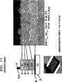
Im Folgenden werden nicht einschränkende Versuchsergebnisse erläutert. In
Aus der obigen Erläuterung geht hervor, dass ein beispielhaftes Verfahren allgemein ausgedrückt eine Niedertemperatur-Vakuumabscheidung mit einem kurzzeitigen Hochtemperaturglühen kombiniert, um auf einem Substrat einen Kesteritabsorber zu bilden, der für Solarzellenanwendungen verwendbar ist. In einer bevorzugten Ausführungsform wird die Niedertemperaturabscheidung durch Zerstäubung und/oder Wärmeverdampfung und/oder Elektronenstrahlverdampfung oder kombinierte Verfahren in einer Hochvakuumumgebung durchgeführt. Wärmeverdampfung ist eine bevorzugte Technik zur Steuerung der Zusammensetzung und zur effizienten Ausnutzung der Metallbestandteile. Das Hochtemperaturglühen kann mit einer Wärmeplatte oder anderen Heizverfahren so durchgeführt werden, dass die Absorberschicht kurzzeitig geglüht wird, bevorzugt innerhalb von dreißig Minuten und noch bevorzugter in zwanzig Minuten oder weniger. Dieses Glühen kann ohne Spezialofen und ohne H2S durchgeführt werden. In einer oder mehreren Ausführungsformen kann die Wärmezufuhr das direkte Zuführen der Wärme zum Substrat
Aus der obigen Erläuterung geht auch hervor, dass ein beispielhaftes Verfahren (zum Beispiel zur Herstellung von Solarzellen) allgemein ausgedrückt aufweist das Bereitstellen eines Substrats, das Aussetzen des Substrats einer Hochvakuumumgebung, das Erwärmen des Substrats auf eine erste Temperatur, das Abscheiden von Kupfer, Zink, Zinn und mindestens einem von Schwefel und Selen durch Wärmeverdampfung, Elektronenstrahlverdampfung und/oder Zerstäubung auf eine Oberfläche des erwärmten Substrats, um eine für Solarzellenanwendungen geeignete Absorberschicht zu bilden, und das Glühen des Substrats bei einer zweiten Temperatur, die wesentlich höher ist als die erste Temperatur. Insbesondere liegt die erste Temperatur zwischen 100 und 200°C, sodass Wiederverdampfungsverluste nicht wesentlich sind und daher nicht problematisch werden, während die zweite Temperatur 300°C oder mehr beträgt, um das Kurzzeitglühen zu erleichtern.From the above discussion, it is also apparent that an exemplary method (for example, for manufacturing solar cells), generally speaking, comprises providing a substrate, exposing the substrate to a high vacuum environment, heating the substrate to a first temperature, depositing copper, zinc , Tin and at least one of sulfur and selenium by heat evaporation, electron beam evaporation and / or sputtering on a surface of the heated substrate to form an absorber layer suitable for solar cell applications, and annealing the substrate at a second temperature substantially higher than the first Temperature. In particular, the first temperature is between 100 and 200 ° C, so that re-evaporation losses are not essential and thus do not become problematic while the second temperature is 300 ° C or more to facilitate the short-time annealing.
Zusätzliche Schritte umfassen das Züchten einer Emitterschicht nach dem Glühen, das Abscheiden einer transparenten Leitoxidschicht auf der Emitterschicht, das Abscheiden eines oberen Metallkontakts auf der transparenten Leitoxidschicht und die Abtrennung der Einheiten, um eine Vielzahl von Solarzellen zu erhalten.Additional steps include growing an emitter layer after annealing, depositing a transparent conductive oxide layer on the emitter layer, depositing an upper metal contact on the transparent conductive oxide layer, and separating the units to obtain a plurality of solar cells.
Ein oder mehrere der oben beschriebenen Verfahren, Techniken und/oder Prozesse können zum Beispiel in der Fertigung von Produkten wie Solarzellen und dergleichen verwendet werden.For example, one or more of the above-described methods, techniques and / or processes may be used in the manufacture of products such as solar cells and the like.
Beispielhafte Details zu Systemen und Herstellungsprodukten Exemplary details of systems and manufacturing products
Wie der Fachmann erkennen wird, können Aspekte (z. B. zur Steuerung eines Abscheidungs-, Glüh-, Herstellungs- oder Testprozesses) der vorliegenden Erfindung als System, Verfahren oder Computerprogrammprodukt ausgeführt werden. Daher können bestimmte Aspekte der vorliegenden Erfindung die Form einer kompletten Hardware-Ausführungsform, einer kompletten Software-Ausführungsform (einschließlich Firmware, speicherresidenter Software, Mikrocode usw.) oder einer Ausführungsform annehmen, die Software- und Hardwareaspekte kombiniert, die hierin alle allgemein als ”Schaltung”, ”Modul” oder ”System” bezeichnet werden können. Überdies können Aspekte der vorliegenden Erfindung die Form eines Computerprogrammprodukts annehmen, das in einem computerlesbaren Medium oder in mehreren computerlesbaren Medien mit einem darauf verkörperten computerlesbaren Programmcode verkörpert ist.As those skilled in the art will appreciate, aspects (eg, for controlling a deposition, annealing, fabrication, or testing process) of the present invention may be embodied as a system, method, or computer program product. Therefore, certain aspects of the present invention may take the form of a complete hardware embodiment, a complete software embodiment (including firmware, memory resident software, microcode, etc.), or an embodiment that combines software and hardware aspects, collectively referred to herein as "circuitry , "Module" or "system". Moreover, aspects of the present invention may take the form of a computer program product embodied in a computer readable medium or in a plurality of computer readable media having computer readable program code embodied thereon.
Eine oder mehrere Ausführungsformen von Teilen der Erfindung oder Elementen davon können in Form einer Vorrichtung realisiert werden, die einen Speicher und mindestens einen Prozessor aufweist, der mit dem Speicher verbunden ist und betreibbar ist, um beispielhafte Verfahrensschritte durchzuführen oder zu erleichtern.One or more embodiments of parts of the invention or elements thereof may be implemented in the form of a device having a memory and at least one processor connected to the memory and operable to perform or facilitate example method steps.
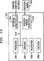
Eine oder mehrere Ausführungsformen können Software verwenden, die auf einem Universalcomputer oder einer Workstation ausgeführt wird. Auf
Schnittstellen für Sensoren (z. B. Druck, Kraft, Temperatur), Betätigungselementen und dergleichen können zur Steuerung eines Glüh-, Herstellungs-, und/oder Testprozesses oder jedes Teils davon bereitgestellt werden.Interfaces for sensors (eg, pressure, force, temperature), actuators, and the like may be provided to control an annealing, manufacturing, and / or testing process, or any part thereof.
Demnach kann Computersoftware mit Befehlen oder Code zur Durchführung der Verfahren der Erfindung, wie hierin beschrieben, in einem oder mehreren der zugehörigen Speichereinheiten (zum Beispiel ROM, fester oder entnehmbarer Speicher) gespeichert sein und, wenn sie verfügbar ist, teilweise oder ganz (zum Beispiel in den RAM) geladen und von einer CPU ausgeführt werden. Solch eine Software kann, ohne darauf beschränkt zu sein, Firmware, residente Software, Mikrocode und dergleichen einschließen.Thus, computer software having instructions or code for carrying out the methods of the invention as described herein may be stored in one or more of the associated memory units (eg, ROM, fixed or removable memory) and, if available, partially or wholly (e.g. in the RAM) and executed by a CPU. Such software may include, but is not limited to, firmware, resident software, microcode and the like.
Ein Datenverarbeitungssystem, das zum Speichern und/oder Ausführen von Programmcode geeignet ist, wird mindestens einen Prozessor
Eingabe-Ausgabe- oder E/A-Geräte (einschließlich, ohne darauf beschränkt zu sein, Tastaturen
Auch Netzwerkadapter wie die Netzwerkschnittstelle
Wie hierin verwendet, einschließlich in den Ansprüchen, weist ein ”Server” ein physisches Datenverarbeitungssystem (zum Beispiel, das System
Wie erwähnt, können Aspekte der vorliegenden Erfindung die Form eines Computerprogrammprodukts annehmen, das in einem computerlesbaren Medium oder in mehreren computerlesbaren Medien mit einem darauf verkörperten computerlesbaren Programmcode verkörpert ist. Jede Kombination eines computerlesbaren Mediums oder mehrerer computerlesbarer Medien kann verwendet werden. Das computerlesbare Medium kann ein computerlesbarer Signalträger oder ein computerlesbares Speichermedium sein. Ein computerlesbares Speichermedium kann zum Beispiel, ohne darauf beschränkt zu sein, ein elektronisches, magnetisches, optisches, elektromagnetisches, Infrarot- oder Halbleiter-System, eine entsprechende Vorrichtung oder Einheit oder jede geeignete Kombination des Vorstehenden sein. Der Speichermedien-Block
Ein computerlesbarer Signalträger kann ein verbreitetes Datensignal mit einem computerlesbaren Programmcode sein, der zum Beispiel im Basisband oder als Teil einer Trägerwelle darin verkörpert ist. Solch ein verbreitetes Signal kann verschiedene Formen annehmen, einschließlich, ohne darauf beschränkt zu sein, elektromagnetisch, optisch oder jede geeignete Kombination daraus. Ein computerlesbarer Signalträger kann jedes computerlesbare Medium sein, das kein computerlesbares Speichermedium ist und ein Programm zur Verwendung durch oder in Verbindung mit einem Befehlsausführungssystem oder einer entsprechenden Vorrichtung oder Einheit übertragen, verbreiten oder transportieren kann.A computer readable signal carrier may be a propagated data signal having computer readable program code embodied therein, for example, in baseband or as part of a carrier wave. Such a propagated signal may take various forms, including, but not limited to, electromagnetically, optically, or any suitable combination thereof. A computer readable signal carrier may be any computer readable medium that is not a computer readable storage medium and that is capable of transmitting, propagating, or transporting a program for use by or in connection with an instruction execution system or device or device.
Der Programmcode, der auf einem computerlesbaren Medium verkörpert ist, kann durch jedes geeignete Medium übertragen werden, einschließlich, ohne darauf beschränkt zu sein, drahtlos, Drahtleitung, Glasfaserkabel, HF usw., oder jede geeignete Kombination des Vorstehenden.The program code, embodied on a computer readable medium, may be transmitted by any suitable medium, including, but not limited to, wireless, wireline, fiber optic, RF, etc., or any suitable combination of the foregoing.
Der Computerprogrammcode zur Durchführung von Operationen für Aspekte der vorliegenden Erfindung kann in jeder Kombination einer oder mehrerer Programmiersprachen geschrieben sein, einschließlich einer objektorientierten Programmiersprache wie Java, Smalltalk, C++ oder dergleichen und konventioneller prozeduraler Programmiersprachen wie die Programmiersprache ”C” oder ähnliche Programmiersprachen. Der Programmcode kann gänzlich auf dem Computer des Benutzers, teilweise auf dem Computer des Benutzers, als eigenständiges Softwarepaket, teilweise auf dem Computer des Benutzers und teilweise auf einem fernen Computer oder gänzlich auf dem fernen Computer oder Server ausgeführt werden. Im letzteren Szenario kann der ferne Computer durch jede Art von Netzwerk einschließlich eines lokalen Netzwerks (LAN) oder eines Weitverkehrsnetzes (WAN) mit dem Computer eines Benutzers verbunden sein, oder die Verbindung kann zu einem externen Computer hergestellt werden (zum Beispiel über das Internet durch einen Internet-Diensteanbieter).The computer program code for performing operations for aspects of the present invention may be written in any combination of one or more programming languages, including an object-oriented programming language such as Java, Smalltalk, C ++ or the like and conventional procedural programming languages such as the "C" programming language or similar programming languages. The program code may be executed entirely on the user's computer, partly on the user's computer, as a standalone software package, partly on the user's computer and partly on a remote computer or entirely on the remote computer or server. In the latter scenario, the remote computer may be connected to a user's computer by any type of network, including a local area network (LAN) or a wide area network (WAN), or the connection may be made to an external computer (for example, over the Internet) an internet service provider).
Aspekte der vorliegenden Erfindung werden hierin Bezug nehmend auf Ablaufpläne und/oder Blockschaubilder von Verfahren, Vorrichtungen (Systemen) und Computerprogrammprodukten gemäß Ausführungsformen der Erfindung beschrieben. Es versteht sich, dass jeder Block der Ablaufpläne und/oder Blockschaubilder und Kombinationen von Blöcken in den Ablaufplänen und/oder Blockschaubildern durch Computerprogrammbefehle realisiert werden können. Diese Computerprogrammbefehle können einem Prozessor eines Universalcomputers, Spezialcomputers oder einer sonstigen programmierbaren Datenverarbeitungsvorrichtung zur Herstellung einer Maschine so bereitgestellt werden, dass die Befehle, die über den Prozessor des Computers oder der sonstigen programmierbaren Datenverarbeitungsvorrichtung ausgeführt werden, Mittel zur Durchführung der Funktionen/Vorgänge ergeben, die im Block oder in Blöcken der Ablaufpläne und/oder Blockschaubilder angegeben sind.Aspects of the present invention are described herein with reference to flowcharts and / or block diagrams of methods, apparatus (systems) and computer program products according to embodiments of the invention. It is understood that each block of the flowcharts and / or block diagrams and combinations of blocks in the flowcharts and / or block diagrams can be realized by computer program instructions. These computer program instructions may be provided to a processor of a general-purpose computer, special purpose computer, or other programmable data processing device for manufacturing a machine such that the instructions executed via the processor of the computer or other programmable data processing device provide means for performing the functions / operations which in the block or in Blocks of flowcharts and / or block diagrams.
Diese Computerprogrammbefehle können auch in einem computerlesbaren Medium gespeichert sein, das einen Computer, eine andere programmierbare Datenverarbeitungsvorrichtung oder sonstige Einheiten anweisen kann, auf eine bestimmte Weise zu funktionieren, sodass die Befehle, die im computerlesbaren Medium gespeichert sind, ein Herstellungsprodukt mit Befehlen ergeben, die die Funktionen/Vorgänge realisieren, die die im Block oder in Blöcken der Ablaufpläne und/oder Blockschaubilder angegeben sind.These computer program instructions may also be stored in a computer readable medium that may instruct a computer, other programmable computing device, or other entity to function in a particular manner so that the instructions stored in the computer readable medium provide a manufacturing product with instructions that implement the functions / operations specified in the block or in blocks of flowcharts and / or block diagrams.
Die Computerprogrammbefehle können auch in einen Computer, in eine andere programmierbare Datenverarbeitungsvorrichtung oder in sonstige Einheiten geladen werden, um die Durchführung einer Reihe von Arbeitsgängen auf dem Computer, der anderen programmierbaren Vorrichtung oder sonstigen Einheiten zu bewirken, um einen computergestützten Prozess zu ergeben, sodass die Befehle, die auf dem Computer oder der sonstigen programmierbaren Vorrichtung ausgeführt werden, Prozesse zur Ausführung der Funktionen/Vorgänge ergeben, die im Block oder in Blöcken der Ablaufpläne und/oder Blockschaubilder angegeben sind.The computer program instructions may also be loaded into a computer, other programmable computing device, or other device to effectuate a series of operations on the computer, other programmable device, or other devices to result in a computer aided process, such that the computer aided processing Instructions executed on the computer or other programmable device result in processes for executing the functions / operations indicated in the block or blocks of the flowcharts and / or block diagrams.
Die Ablaufpläne und Blockschaubilder in den Figuren veranschaulichen die Architektur, die Funktionalität und den Betrieb möglicher Implementierungen von Systemen, Verfahren und Computerprogrammprodukten nach verschiedenen Ausführungsformen der vorliegenden Erfindung. In diesem Zusammenhang kann jeder Block in den Ablaufplänen oder Blockschaubildern ein Codemodul, ein Codesegment oder einen Codeteil darstellen, das einen oder mehrere ausführbare Befehle zur Realisierung der spezifizierten logischen Funktion(en) umfasst. Es ist auch anzumerken, dass die in den Blöcken genannten Funktionen in einigen alternativen Realisierungen in einer anderen Reihenfolge als der in der Figur genannten auftreten können. Zum Beispiel können zwei Blöcke, die aufeinanderfolgend dargestellt sind, tatsächlich im Wesentlichen gleichzeitig ausgeführt werden, oder die Blöcke können abhängig von der beteiligten Funktionalität manchmal in umgekehrter Reihenfolge ausgeführt werden. Es ist auch anzumerken, dass jeder Block der Blockschaubildern und/oder Ablaufplänen und Kombinationen von Blöcken in den Blockschaubildern und/oder Ablaufplänen durch Systeme auf der Basis von Spezialhardware, die die spezifizierten Funktionen oder Vorgänge durchführen, oder durch Kombinationen von Spezialhardware und Computerbefehlen ausgeführt werden können.The flowcharts and block diagrams in the figures illustrate the architecture, functionality, and operation of possible implementations of systems, methods, and computer program products according to various embodiments of the present invention. In this context, each block in the flowcharts or block diagrams may represent a code module, a code segment, or a code part that includes one or more executable instructions for realizing the specified logical function (s). It should also be noted that in some alternative implementations the functions mentioned in the blocks may occur in a different order than that mentioned in the figure. For example, two blocks that are displayed in succession may in fact be executed substantially simultaneously, or the blocks may sometimes be executed in reverse order depending on the functionality involved. It should also be noted that each block of block diagrams and / or flowcharts and combinations of blocks in the block diagrams and / or flowcharts are executed by systems based on specialized hardware performing the specified functions or operations, or by combinations of specialized hardware and computer instructions can.
Es ist anzumerken, dass jedes der Verfahren, die hierin beschrieben werden, einen zusätzlichen Schritt des Bereitstellens eines Systems umfassen kann, das einzelne Softwaremodule aufweist, die auf einem computerlesbaren Speichermedium verkörpert sind; die Module können zum Beispiel Module einschließen, um das Glühen, die Herstellung oder das Testen wie hierin beschrieben durchzuführen, zu steuern und/oder zu erleichtern (z. B. Steuerung einer Wärmequelle für das Glühen). Die Verfahrensschritte können dann wie oben beschrieben mit getrennten Softwaremodulen und/oder Untermodulen des Systems durchgeführt werden, die auf einem oder mehreren Hardware-Prozessoren
In jedem Fall versteht es sich, dass die Komponenten, die hierin veranschaulicht werden, in verschiedenen Formen von Hardware, Software oder Kombinationen daraus realisiert werden können; zum Beispiel anwendungsspezifische integrierte Schaltung(en) (ASICS), Funktionsschaltungen, ein oder mehrere auf geeignete Weise programmierte Universaldigitalcomputer mit zugehörigem Speicher und dergleichen. Aufgrund der Lehren der Erfindung, die hierin gegeben wurden, wird der Fachmann in der Lage sein, andere Realisierungen der Komponenten der Erfindung in Betracht zu ziehen.In any event, it will be understood that the components illustrated herein may be implemented in various forms of hardware, software, or combinations thereof; For example, application specific integrated circuit (s) (ASICS), functional circuits, one or more suitably programmed universal digital computers with associated memory, and the like. Due to the teachings of the invention given herein, those skilled in the art will be able to contemplate other implementations of the components of the invention.
Die hierin verwendete Terminologie dient lediglich der Beschreibung bestimmter Ausführungsformen und soll die Erfindung in keiner Weise einschränken. Die Singularformen ”ein, eine” und ”der, die, das”, wie sie hierin verwendet werden, schließen auch die Pluralformen ein, sofern der Kontext nicht eindeutig etwas anderes besagt. Ferner versteht es sich, dass die Ausdrücke ”aufweist” und/oder ”aufweisend,” wenn sie in dieser Patentschrift verwendet werden, das Vorhandensein der genannten Eigenschaften, ganzer Zahlen, Schritte, Operationen, Elemente und/oder Komponenten angeben, aber das Vorhandensein oder den Zusatz einer oder mehrerer anderer Eigenschaften, ganzer Zahlen, Schritte, Operationen, Elemente, Komponenten und/oder Gruppen davon nicht ausschließen.The terminology used herein is for the purpose of describing particular embodiments only and is not intended to limit the invention in any way. The singular forms "a, a" and "the, the" as used herein also include the plural forms unless the context clearly dictates otherwise. Further, it should be understood that the terms "having" and / or "having," when used in this specification, indicate the presence of said features, integers, steps, operations, elements and / or components, but the presence or absence of do not preclude the addition of one or more other properties, integers, steps, operations, elements, components, and / or groups thereof.
Die entsprechenden Strukturen, Materialien, Vorgänge und Entsprechungen aller Mittel oder Schritt-plus-Funktion-Elemente in den folgenden Ansprüchen sollen alle Strukturen, Materialien und Vorgänge zur Durchführung der Funktion in Kombination mit anderen beanspruchten Elementen einschließen, wie spezifisch beansprucht. Die Beschreibung der vorliegenden Erfindung soll der Veranschaulichung und Beschreibung dienen, ohne aber erschöpfend oder auf die Erfindung in der offenbarten Form beschränkt zu sein. Dem Fachmann werden viele Modifikationen und Varianten einfallen, ohne vom Umfang und Geist der Erfindung abzuweichen.The corresponding structures, materials, acts, and equivalents of all means or step plus function elements in the following claims are intended to include all structures, materials, and acts of performing the function in combination with other claimed elements, as specifically claimed. The description of the present invention is intended to be illustrative and descriptive, but not exhaustive or limited to the invention in the form disclosed. Many modifications and variations will occur to those skilled in the art without departing from the scope and spirit of the invention.
Die Ausführungsform wurde gewählt und beschrieben, um die Prinzipien der Erfindung und die praktische Anwendung am besten zu erklären, und um anderen Fachleuten das Verständnis der Erfindung für verschiedene Ausführungsformen mit verschiedenen Modifikationen zu ermöglichen, wie sie für die vorgesehene spezifische Anwendung geeignet sind.The embodiment has been chosen and described in order to best explain the principles of the invention and the practical application, and to enable others skilled in the art to understand the invention for various embodiments with various modifications as appropriate to the intended specific application.
Claims (25)
Applications Claiming Priority (3)
| Application Number | Priority Date | Filing Date | Title |
|---|---|---|---|
| US12/911,833 US8440497B2 (en) | 2010-10-26 | 2010-10-26 | Fabricating kesterite solar cells and parts thereof |
| US12/911,833 | 2010-10-26 | ||
| PCT/EP2011/068254 WO2012055737A2 (en) | 2010-10-26 | 2011-10-19 | Kesterite layer fabrication for thin film solar cells |
Publications (1)
| Publication Number | Publication Date |
|---|---|
| DE112011102890T5 true DE112011102890T5 (en) | 2013-06-06 |
Family
ID=44897726
Family Applications (1)
| Application Number | Title | Priority Date | Filing Date |
|---|---|---|---|
| DE112011102890T Ceased DE112011102890T5 (en) | 2010-10-26 | 2011-10-19 | Kesterite layer production for thin-film solar cells |
Country Status (5)
| Country | Link |
|---|---|
| US (1) | US8440497B2 (en) |
| JP (1) | JP2014502039A (en) |
| CN (1) | CN103180969A (en) |
| DE (1) | DE112011102890T5 (en) |
| WO (1) | WO2012055737A2 (en) |
Families Citing this family (14)
| Publication number | Priority date | Publication date | Assignee | Title |
|---|---|---|---|---|
| US20120318361A1 (en) * | 2011-06-20 | 2012-12-20 | Alliance For Sustainable Energy, Llc | Manufacturing thin films with chalcogen species with independent control over doping and bandgaps |
| US20130217211A1 (en) * | 2012-02-21 | 2013-08-22 | Aqt Solar, Inc. | Controlled-Pressure Process for Production of CZTS Thin-Films |
| US8586457B1 (en) * | 2012-05-17 | 2013-11-19 | Intermolecular, Inc. | Method of fabricating high efficiency CIGS solar cells |
| US9153729B2 (en) * | 2012-11-26 | 2015-10-06 | International Business Machines Corporation | Atomic layer deposition for photovoltaic devices |
| US9349906B2 (en) | 2014-09-27 | 2016-05-24 | International Business Machines Corporation | Anneal techniques for chalcogenide semiconductors |
| US9917216B2 (en) * | 2014-11-04 | 2018-03-13 | International Business Machines Corporation | Flexible kesterite photovoltaic device on ceramic substrate |
| CN105679878A (en) * | 2014-11-17 | 2016-06-15 | 中国电子科技集团公司第十八研究所 | Method for preparing absorption layer of CZTSSe thin film solar cell by co-evaporation |
| US10032949B2 (en) * | 2015-11-09 | 2018-07-24 | International Business Machines Corporation | Photovoltaic device based on Ag2ZnSn(S,Se)4 absorber |
| CN105470113B (en) * | 2015-11-20 | 2018-07-10 | 中国电子科技集团公司第十八研究所 | A kind of preparation method of CZTSSe absorption layer of thin film solar cell |
| KR20170097440A (en) * | 2016-02-18 | 2017-08-28 | 전영권 | Solar cells and manufacturing method for the same |
| PL241410B1 (en) * | 2019-02-11 | 2022-09-26 | Akademia Górniczo-Hutnicza im. Stanisława Staszica w Krakowie | Method for producing powder kesterite of Cu₂SnZnS₄ type |
| PL241416B1 (en) * | 2019-02-11 | 2022-09-26 | Akademia Górniczo-Hutnicza im. Stanisława Staszica w Krakowie | Method for producing powder kesterite of Cu₂SnZnS₄ type, intended for production of active layers in thin film photovoltaic cells |
| CN110867383B (en) * | 2019-11-21 | 2023-05-30 | 中国电子科技集团公司第十八研究所 | Method for preparing copper zinc tin sulfide film absorption layer by three-step vulcanization process |
| CN114864752A (en) * | 2022-06-15 | 2022-08-05 | 金陵科技学院 | Method for improving residual stress of absorption layer of flexible CZTSSe thin-film solar cell and application |
Family Cites Families (7)
| Publication number | Priority date | Publication date | Assignee | Title |
|---|---|---|---|---|
| JP4543162B2 (en) * | 2001-09-05 | 2010-09-15 | 独立行政法人産業技術総合研究所 | ZnOSSe mixed crystal semiconductor |
| US7518207B1 (en) * | 2004-03-19 | 2009-04-14 | The United States Of America As Represented By The Secretary Of The Navy | Molecular beam epitaxy growth of ternary and quaternary metal chalcogenide films |
| JP5246839B2 (en) * | 2006-08-24 | 2013-07-24 | 独立行政法人産業技術総合研究所 | Semiconductor thin film manufacturing method, semiconductor thin film manufacturing apparatus, photoelectric conversion element manufacturing method, and photoelectric conversion element |
| JP2010245238A (en) * | 2009-04-03 | 2010-10-28 | Promatic Kk | Photoelectric conversion device and method of manufacturing the same, as well as method of manufacturing sulfide sintered compact target |
| US20110017289A1 (en) * | 2009-07-24 | 2011-01-27 | Electronics And Telecommunications Research Institute | Cigs solar cell and method of fabricating the same |
| EP2519977A4 (en) * | 2009-12-28 | 2016-05-18 | Nanosolar Inc | Low cost solar cells formed using a chalcogenization rate modifier |
| CN101824638B (en) * | 2010-05-06 | 2012-12-19 | 深圳丹邦投资集团有限公司 | Method for electrochemically depositing copper-zinc-tin-selenium semiconductor thin film material |
-
2010
- 2010-10-26 US US12/911,833 patent/US8440497B2/en active Active
-
2011
- 2011-10-19 DE DE112011102890T patent/DE112011102890T5/en not_active Ceased
- 2011-10-19 JP JP2013535365A patent/JP2014502039A/en active Pending
- 2011-10-19 WO PCT/EP2011/068254 patent/WO2012055737A2/en active Application Filing
- 2011-10-19 CN CN2011800510920A patent/CN103180969A/en active Pending
Also Published As
| Publication number | Publication date |
|---|---|
| WO2012055737A2 (en) | 2012-05-03 |
| CN103180969A (en) | 2013-06-26 |
| US8440497B2 (en) | 2013-05-14 |
| US20120100664A1 (en) | 2012-04-26 |
| WO2012055737A3 (en) | 2012-12-27 |
| JP2014502039A (en) | 2014-01-23 |
Similar Documents
| Publication | Publication Date | Title |
|---|---|---|
| DE112011102890T5 (en) | Kesterite layer production for thin-film solar cells | |
| DE102009045929A1 (en) | Solar cell and method for producing the same | |
| EP0715358B1 (en) | Process for fabricating a solar cell with a chalcopyrite absorbing layer and solar cell so produced | |
| DE102011018268A1 (en) | Single junction CIGS / CIC solar modules | |
| DE102012103243B4 (en) | Method for changing the laser intensity over time during the scribing of a photovoltaic device | |
| DE112012003297T5 (en) | Cover layers for improved crystallization | |
| DE102012100795B4 (en) | Superstrate solar cell and process for its manufacture | |
| DE112009002289T5 (en) | Thin film sodium species barrier layer method and structure for a CIGS based thin film photovoltaic cell | |
| DE112008003144T5 (en) | Layer structure of CIS solar cell, integrated structure of CIS thin-film solar cell and its manufacturing process | |
| DE112009002238T5 (en) | Method and structure for a thin-film photovoltaic tandem cell | |
| DE202004021800U1 (en) | Semiconductor films of a quaternary or higher alloy of group I-III-VI | |
| DE102012108901A1 (en) | Method and system for producing chalcogenide semiconductor materials using sputtering and evaporation functions | |
| DE10351674A1 (en) | Electronic component and method for its production | |
| DE102011056565A1 (en) | A method of forming a cadmium tin oxide layer and a photovoltaic device | |
| DE102011054716A1 (en) | Mixed sputtering target of cadmium sulfide and cadmium telluride and method of use | |
| DE102013104232A1 (en) | solar cell | |
| DE102012109883A1 (en) | Process for producing a thin-film solar cell with buffer-free manufacturing process | |
| DE112010004876T5 (en) | Process for producing a CIS-based thin-film solar cell | |
| US10319871B2 (en) | Photovoltaic device based on Ag2ZnSn(S,Se)4 absorber | |
| DE102011056639A1 (en) | Method for producing a transparent conductive oxide layer and a photovoltaic device | |
| DE102012100259A1 (en) | Method for producing a semiconducting film and photovoltaic device | |
| DE112012001058T5 (en) | Tandem solar cell with improved absorption material | |
| DE102012104616B4 (en) | A method of forming a window layer in a cadmium telluride based thin film photovoltaic device | |
| EP2162563B1 (en) | Temperature-resistant tco layer and production method therefor | |
| DE102009054630B4 (en) | Method for producing a photovoltaic device |
Legal Events
| Date | Code | Title | Description |
|---|---|---|---|
| R012 | Request for examination validly filed | ||
| R081 | Change of applicant/patentee |
Owner name: GLOBALFOUNDRIES U.S. INC., SANTA CLARA, US Free format text: FORMER OWNER: INTERNATIONAL BUSINESS MACHINES CORPORATION, ARMONK, N.Y., US Owner name: GLOBALFOUNDRIES INC., KY Free format text: FORMER OWNER: INTERNATIONAL BUSINESS MACHINES CORPORATION, ARMONK, N.Y., US |
|
| R082 | Change of representative |
Representative=s name: RICHARDT PATENTANWAELTE PARTG MBB, DE |
|
| R081 | Change of applicant/patentee |
Owner name: GLOBALFOUNDRIES U.S. INC., SANTA CLARA, US Free format text: FORMER OWNER: GLOBALFOUNDRIES US 2 LLC (N.D.GES.DES STAATES DELAWARE), HOPEWELL JUNCTION, N.Y., US Owner name: GLOBALFOUNDRIES INC., KY Free format text: FORMER OWNER: GLOBALFOUNDRIES US 2 LLC (N.D.GES.DES STAATES DELAWARE), HOPEWELL JUNCTION, N.Y., US |
|
| R082 | Change of representative |
Representative=s name: RICHARDT PATENTANWAELTE PARTG MBB, DE |
|
| R016 | Response to examination communication | ||
| R016 | Response to examination communication | ||
| R002 | Refusal decision in examination/registration proceedings | ||
| R003 | Refusal decision now final | ||
| R081 | Change of applicant/patentee |
Owner name: GLOBALFOUNDRIES U.S. INC., SANTA CLARA, US Free format text: FORMER OWNER: GLOBALFOUNDRIES INC., GRAND CAYMAN, KY |
|
| R082 | Change of representative |
Representative=s name: RICHARDT PATENTANWAELTE PARTG MBB, DE |