DE112010003495B4 - Tunnel field effect transistor structure and method of manufacture - Google Patents
Tunnel field effect transistor structure and method of manufacture Download PDFInfo
- Publication number
- DE112010003495B4 DE112010003495B4 DE112010003495T DE112010003495T DE112010003495B4 DE 112010003495 B4 DE112010003495 B4 DE 112010003495B4 DE 112010003495 T DE112010003495 T DE 112010003495T DE 112010003495 T DE112010003495 T DE 112010003495T DE 112010003495 B4 DE112010003495 B4 DE 112010003495B4
- Authority
- DE
- Germany
- Prior art keywords
- field effect
- effect transistor
- transistor structure
- semiconductor material
- semiconductor
- Prior art date
- Legal status (The legal status is an assumption and is not a legal conclusion. Google has not performed a legal analysis and makes no representation as to the accuracy of the status listed.)
- Active
Links
- 230000005669 field effect Effects 0.000 title claims abstract description 33
- 238000000034 method Methods 0.000 title claims description 21
- 238000004519 manufacturing process Methods 0.000 title description 3
- 239000004065 semiconductor Substances 0.000 claims abstract description 66
- 239000000463 material Substances 0.000 claims abstract description 46
- 238000005253 cladding Methods 0.000 claims abstract description 25
- 230000005641 tunneling Effects 0.000 claims abstract description 18
- 239000012212 insulator Substances 0.000 claims abstract description 16
- 239000002070 nanowire Substances 0.000 claims description 24
- 229910000673 Indium arsenide Inorganic materials 0.000 claims description 6
- RPQDHPTXJYYUPQ-UHFFFAOYSA-N indium arsenide Chemical compound [In]#[As] RPQDHPTXJYYUPQ-UHFFFAOYSA-N 0.000 claims description 6
- OKTJSMMVPCPJKN-UHFFFAOYSA-N Carbon Chemical compound [C] OKTJSMMVPCPJKN-UHFFFAOYSA-N 0.000 claims description 3
- 239000002041 carbon nanotube Substances 0.000 claims description 3
- 229910021393 carbon nanotube Inorganic materials 0.000 claims description 3
- 239000007769 metal material Substances 0.000 claims 4
- 238000010586 diagram Methods 0.000 description 14
- 239000002184 metal Substances 0.000 description 12
- 230000005283 ground state Effects 0.000 description 5
- 230000004888 barrier function Effects 0.000 description 2
- 230000000295 complement effect Effects 0.000 description 2
- 230000000694 effects Effects 0.000 description 2
- 230000005684 electric field Effects 0.000 description 2
- 229910044991 metal oxide Inorganic materials 0.000 description 2
- 150000004706 metal oxides Chemical class 0.000 description 2
- 239000003595 mist Substances 0.000 description 2
- 229910052710 silicon Inorganic materials 0.000 description 2
- 230000007704 transition Effects 0.000 description 2
- 101100232929 Caenorhabditis elegans pat-4 gene Proteins 0.000 description 1
- 238000003491 array Methods 0.000 description 1
- 238000005452 bending Methods 0.000 description 1
- 230000008859 change Effects 0.000 description 1
- 239000002800 charge carrier Substances 0.000 description 1
- 239000002131 composite material Substances 0.000 description 1
- 239000004020 conductor Substances 0.000 description 1
- 238000010276 construction Methods 0.000 description 1
- 230000007547 defect Effects 0.000 description 1
- 230000001419 dependent effect Effects 0.000 description 1
- 239000002019 doping agent Substances 0.000 description 1
- 238000004377 microelectronic Methods 0.000 description 1
- 238000004806 packaging method and process Methods 0.000 description 1
- 230000008569 process Effects 0.000 description 1
- 239000000700 radioactive tracer Substances 0.000 description 1
- 230000009467 reduction Effects 0.000 description 1
- 238000001338 self-assembly Methods 0.000 description 1
- 239000010703 silicon Substances 0.000 description 1
- 239000007787 solid Substances 0.000 description 1
- 230000003068 static effect Effects 0.000 description 1
- 238000000859 sublimation Methods 0.000 description 1
- 230000008022 sublimation Effects 0.000 description 1
- 239000000758 substrate Substances 0.000 description 1
- 239000011800 void material Substances 0.000 description 1
Images


Classifications
-
- B—PERFORMING OPERATIONS; TRANSPORTING
- B82—NANOTECHNOLOGY
- B82Y—SPECIFIC USES OR APPLICATIONS OF NANOSTRUCTURES; MEASUREMENT OR ANALYSIS OF NANOSTRUCTURES; MANUFACTURE OR TREATMENT OF NANOSTRUCTURES
- B82Y10/00—Nanotechnology for information processing, storage or transmission, e.g. quantum computing or single electron logic
-
- H—ELECTRICITY
- H01—ELECTRIC ELEMENTS
- H01L—SEMICONDUCTOR DEVICES NOT COVERED BY CLASS H10
- H01L29/00—Semiconductor devices adapted for rectifying, amplifying, oscillating or switching, or capacitors or resistors with at least one potential-jump barrier or surface barrier, e.g. PN junction depletion layer or carrier concentration layer; Details of semiconductor bodies or of electrodes thereof ; Multistep manufacturing processes therefor
- H01L29/02—Semiconductor bodies ; Multistep manufacturing processes therefor
- H01L29/06—Semiconductor bodies ; Multistep manufacturing processes therefor characterised by their shape; characterised by the shapes, relative sizes, or dispositions of the semiconductor regions ; characterised by the concentration or distribution of impurities within semiconductor regions
- H01L29/0657—Semiconductor bodies ; Multistep manufacturing processes therefor characterised by their shape; characterised by the shapes, relative sizes, or dispositions of the semiconductor regions ; characterised by the concentration or distribution of impurities within semiconductor regions characterised by the shape of the body
- H01L29/0665—Semiconductor bodies ; Multistep manufacturing processes therefor characterised by their shape; characterised by the shapes, relative sizes, or dispositions of the semiconductor regions ; characterised by the concentration or distribution of impurities within semiconductor regions characterised by the shape of the body the shape of the body defining a nanostructure
-
- H—ELECTRICITY
- H01—ELECTRIC ELEMENTS
- H01L—SEMICONDUCTOR DEVICES NOT COVERED BY CLASS H10
- H01L29/00—Semiconductor devices adapted for rectifying, amplifying, oscillating or switching, or capacitors or resistors with at least one potential-jump barrier or surface barrier, e.g. PN junction depletion layer or carrier concentration layer; Details of semiconductor bodies or of electrodes thereof ; Multistep manufacturing processes therefor
- H01L29/66—Types of semiconductor device ; Multistep manufacturing processes therefor
- H01L29/68—Types of semiconductor device ; Multistep manufacturing processes therefor controllable by only the electric current supplied, or only the electric potential applied, to an electrode which does not carry the current to be rectified, amplified or switched
- H01L29/70—Bipolar devices
- H01L29/72—Transistor-type devices, i.e. able to continuously respond to applied control signals
- H01L29/739—Transistor-type devices, i.e. able to continuously respond to applied control signals controlled by field-effect, e.g. bipolar static induction transistors [BSIT]
- H01L29/7391—Gated diode structures
Abstract
Tunnelfeldeffekttransistor-Struktur mit einem indirekt induzierten Tunnelemitter, welcher das folgende umfasst:
einen äußeren Mantel, welcher zumindest teilweise ein längliches Kernelement umgibt, wobei das längliche Kernelement aus einem ersten Halbleitermaterial gebildet ist;
eine Isolatorschicht, welche zwischen dem äußeren Mantel und dem Kernelement angeordnet ist;
wobei der äußere Mantel an einer Stelle angeordnet ist, die einer Source-Zone der Tunnelfeldeffekttransistor-Struktur entspricht; und
einen Source-Kontakt, der den äußeren Mantel mit dem Kernelement kurzschließt;
wobei der äußere Mantel so aufgebaut ist, dass er in die Source-Zone des Kernelements eine Ladungsträgerkonzentration einführt, die zum Tunneln in eine Kanalzone der Tunnelfeldeffekttransistor-Struktur während eines EIN-Zustands ausreicht.Tunnel field effect transistor structure having an indirectly induced tunnel emitter comprising:
an outer jacket at least partially surrounding an elongated core member, the elongated core member being formed from a first semiconductor material;
an insulator layer disposed between the outer jacket and the core member;
wherein the outer cladding is disposed at a location corresponding to a source region of the tunneling field effect transistor structure; and
a source contact shorting the outer jacket to the core element;
wherein the outer cladding is configured to introduce into the source region of the core element a carrier concentration sufficient to tunnel into a channel region of the tunneling field effect transistor structure during an ON state.

Description
ALLGEMEINER STAND DER TECHNIKGENERAL PRIOR ART
Die vorliegende Erfindung betrifft allgemein Strukturen von Halbleitereinheiten und insbesondere einen indirekt induzierten Tunnelemitter für Tunnelfeldeffekttransistor(TFET)-Einheiten und ein Verfahren zu deren Herstellung.The present invention relates generally to semiconductor device structures, and more particularly to an indirectly induced tunnel emitter for tunnel field effect transistor (TFET) devices and a method of making the same.
Mikroelektronische Einheiten werden typischerweise als integrierte Schaltungen auf Halbleitersubstraten hergestellt, welche Komplementär-Metalloxid-Halbleiter(CMOS)-Feldeffekttransistoren als eines ihrer Kernelemente umfassen. Mit der Zeit werden die Abmessungen und Betriebsspannungen der CMOS-Transistoren immer weiter verringert oder maßstäblich verkleinert, um eine immer höhere Leistungsfähigkeit und Packungsdichte der integrierten Schaltungen zu erhalten.Microelectronic devices are typically fabricated as integrated circuits on semiconductor substrates that include complementary metal oxide semiconductor (CMOS) field effect transistors as one of their core elements. Over time, the dimensions and operating voltages of the CMOS transistors continue to be reduced or scaled down to provide increased performance and packaging density of the integrated circuits.
Eines der Probleme, die durch die maßstäbliche Verkleinerung der CMOS-Transistoren entstehen, ist es jedoch, dass der Gesamtstromverbrauch der Einheiten weiter steigt. Dies liegt teilweise daran, dass Leckströme ansteigen (z. B. aufgrund von Kurzkanaleffekten), und auch daran, dass es schwierig wird, die Versorgungsspannung weiter zu verringern. Letzteres liegt wiederum hauptsächlich an der Tatsache, dass die inverse Unterschwellsteigung auf (mindestens) 60 Millivolt(mV)/Dekade begrenzt ist, so dass für das Schalten des Transistors aus dem AUS- in den EIN-Zustand eine bestimmte Spannungsänderung und deswegen eine minimale Versorgungsspannung erforderlich ist.However, one of the problems caused by the scaling down of the CMOS transistors is that the total power consumption of the units continues to increase. This is partly because leakage currents are increasing (eg due to short channel effects) and also because it is becoming difficult to further reduce the supply voltage. The latter, in turn, is mainly due to the fact that the inverse subliminal slope is limited to (at least) 60 millivolts (mV) / decade, so that switching the transistor from the off to on state requires a certain voltage change and therefore a minimum supply voltage is required.
Demgemäß sind Tunnelfeldeffekttransistoren (TFETs) wegen der fehlenden Kurzkanaleffekte und deswegen, weil die Unterschwellsteigung weniger als 60 mV/Dekade, die physikalische Grenze herkömmlicher Metalloxid-Halbleiter-Feldeffekttransistoren (MOSFETs), betragen kann, wodurch potenziell niedrigere Versorgungsspannungen angewendet werden können, als „Nachfolger” der MOSFETs beworben worden. Andererseits weisen TFETs typischerweise niedrige Ströme im eingeschalteten Zustand auf, was einen Nachteil bedeutet, der mit dem hohen Widerstand der Tunnelbarriere in Zusammenhang steht.Accordingly, tunnel field effect transistors (TFETs) are because of the lack of short channel effects, and because the subliminal slope may be less than 60 mV / decade, the physical limit of conventional metal oxide semiconductor field effect transistors (MOSFETs), whereby potentially lower supply voltages can be applied as "followers "The MOSFETs have been advertised. On the other hand, TFETs typically have low currents in the on state, which means a disadvantage associated with the high resistance of the tunnel barrier.
p-Kanal und n-Kanal Nanodrähte mit homogener Zusammensetzung, Nanodrähte umfassende Heterostrukturen, Methoden zum Herstellen von auf Nanodrähte basierten Anordnungen von Geräten und integrierten Schaltkreisen und ein Konzept einer Nanodrahtkreuztraverse sind in der „Nanowire transistor performance limits and applications” offenbart („Nanowire transistor performance limits and applications”, IEEE transactions on electron devices, Seiten 2859–2876, Band 55, Nr. 11, November 2008).Homogeneous composite p-channel and n-channel nanowires, heterostructures comprising nanowires, methods of fabricating devices and integrated circuit nanowire-based arrays, and a nanowire crossbar concept are disclosed in the "Nanowire transistor performance limits and applications" ("Nanowire transistor performance limits and applications ", IEEE transactions on electron devices, pages 2859-2876, volume 55, no. 11, November 2008).
Selbstanordnung von Halbleiter Nanodrähten zur Herstellung von integrierten Schaltkreisen ist in der „Nanowire-based onedimensional electronics” offenbart. („Nanowire-based onedimensional electronics”, Materalstoday, Seiten 28–35, Band 55, Nr. 9, November 2010).Semiconductor self-assembly Nanowires for integrated circuit fabrication are disclosed in Nanowire-based onedimensional electronics. ("Nanowire-based onedimensional electronics", Materalstoday, pp. 28-35, Vol. 55, No. 9, November 2010).
Die
KURZDARSTELLUNG DER ERFINDUNGBRIEF SUMMARY OF THE INVENTION
In einer beispielhaften Ausführungsform umfasst ein indirekt induzierter Tunnelemitter für eine Struktur eines Tunnelfeldeffekttransistors (TFET) einen äußeren Mantel, der zumindest teilweise ein längliches Kernelement umgibt, wobei das längliche Kernelement aus einem ersten Halbleitermaterial gebildet ist; eine Isolatorschicht, die zwischen dem äußeren Mantel und dem Kernelement angeordnet ist; wobei der äußere Mantel an einer Stelle angeordnet ist, die einer Source-Zone der TFET-Struktur entspricht; und einen Source-Kontakt, der den äußeren Mantel mit dem Kernelement kurzschließt; wobei der äußere Mantel so aufgebaut ist, dass er in die Source-Zone des Kernelements eine Ladungsträgerkonzentration einführt, die zum Tunneln in eine Kanalzone der TFET-Struktur während eines EIN-Zustands ausreicht.In an exemplary embodiment, an indirectly induced tunnel emitter for a tunnel field effect transistor (TFET) structure includes an outer cladding at least partially surrounding an elongated core element, the elongate core element being formed from a first semiconductor material; an insulator layer disposed between the outer jacket and the core member; wherein the outer cladding is disposed at a location corresponding to a source region of the TFET structure; and a source contact shorting the outer clad to the core member; wherein the outer cladding is configured to introduce into the source region of the core element a carrier concentration sufficient to tunnel into a channel region of the TFET structure during an ON state.
In einer anderen Ausführungsform umfasst ein Verfahren zum Bilden eines indirekt induzierten Tunnelemitters für eine Tunnelfeldeffekttransistor(TFET)-Struktur das Bilden eines länglichen Kernelements aus einem ersten Halbleitermaterial; das Bilden einer Isolatorschicht, die das Kernelement zumindest teilweise umgibt; das Bilden eines äußeren Mantels, der die Isolatorschicht zumindest teilweise an einer Stelle umgibt, die einer Source-Zone der TFET-Struktur entspricht; und das Bilden eines Source-Kontakts, der den äußeren Mantel mit dem Kernelement kurzschließt; wobei der äußere Mantel so aufgebaut ist, dass er in die Source-Zone des Kernelements eine Ladungsträgerkonzentration einführt, die zum Tunneln in eine Kanalzone der TFET-Struktur während eines EIN-Zustands ausreicht.In another embodiment, a method for forming an indirectly induced tunneling emitter for a tunnel field effect transistor (TFET) structure comprises forming an elongated core element from a first semiconductor material; forming an insulator layer at least partially surrounding the core element; forming an outer cladding at least partially surrounding the insulator layer at a location corresponding to a source region of the TFET structure; and forming a source contact shorting the outer clad to the core member; wherein the outer cladding is configured to introduce into the source region of the core element a carrier concentration sufficient to tunnel into a channel region of the TFET structure during an ON state.
KURZE BESCHREIBUNG DER VERSCHIEDENEN ZEICHNUNGENBRIEF DESCRIPTION OF THE SEVERAL DRAWINGS
Die beispielhaften Zeichnungen zeigen das Folgende, wobei in den verschiedenen Figuren gleiche Elemente gleiche Bezugszahlen aufweisen:The exemplary drawings show the following, wherein in the various figures the same elements have the same reference numerals:
DETAILLIERTE BESCHREIBUNGDETAILED DESCRIPTION
Wie oben angeführt, hat der TFET in den letzten Jahren großes Interesse als möglicher Kandidat zur Verwendung in Elektroniken niedriger Leistungsaufnahme geweckt. Typischerweise werden zum Beispiel in einem n-Kanal-TFET Elektronen vom oberen Bereich des Valenzbandes in der Source-Zone der Einheit in den unteren Bereich des Leitungsbandes im Kanal der Einheit injiziert.
Der Erfindung liegt die Aufgabe zu Grunde ein verbessertes Verfahren zum Bilden einer Tunnelfeldeffekttransistor-Struktur mit einem indirekt indizierten Tunnelemitter sowie eine entsprechende Tunnelfeldeffekttransistor-Struktur mit einem indirekt induzierten Tunnelemitter zu schaffen.The invention is based on the object to provide an improved method for forming a tunnel field effect transistor structure with an indirectly indexed tunnel emitter and a corresponding tunnel field effect transistor structure with an indirectly induced tunnel emitter.
Erfindungsgemäß wird die Aufgabe gelöst durch die Gegenstände der unabhängigen Patentansprüche 1 und 15. Bevorzugte Ausführungsformen der Erfindung sind in den abhängigen Patentansprüchen angegeben.According to the invention the object is solved by the subject matters of independent claims 1 and 15. Preferred embodiments of the invention are specified in the dependent claims.
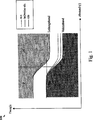
Ein Typ der Übergangsanordnung für eine TFET-Einheit ist als Heteroübergangsaufbau mit versetzt ausgerichteten Bändern bekannt, veranschaulicht in den Banddiagrammen der
Ein Hauptziel der Verwendung von TFETs ist es, ein Schalten von EIN nach AUS über einen viel kleineren Spannungsbereich als bei einem herkömmlichen FET zu erreichen. Dies wird dadurch realisiert, dass eine herkömmliche n-leitende Source-Zone, die in einem NFET benutzt wird, durch eine p-leitende Tunnel-Source-Zone ersetzt wird (hierin auch als „Emitter” bezeichnet), wobei der obere Bereich des Valenzbandes den Wärmeausläufer der Fermifunktion abschneidet, der in der n-leitenden Source-Zone vorliegt, wodurch eine inverse Unterschwellsteigung S von weniger als 60 mV/dek bei Raumtemperatur ermöglicht wird, wobei s = [d(log10ID)/dVG]–1, wobei ID für den Drain-Strom steht und VG für die Gate-Spannung steht.A major goal of using TFETs is to achieve ON to OFF switching over a much smaller voltage range than a conventional FET. This is accomplished by replacing a conventional n-type source region used in an NFET with a p-type tunnel source region (also referred to herein as an "emitter"), the upper region of the valence band cuts off the heat tracer of the Fermi function present in the n-type source region, allowing for an inverse sublimation slope S of less than 60 mV / dec at room temperature, where s = [d (log 10 I D ) / dV G ] - 1 , where I D is the drain current and V G is the gate voltage.
Andererseits veranschaulichen die Banddiagramme der
Obwohl eine solche Bandkrümmung durch das Vorliegen einer hohen Dotierstoffkonzentration in der Source-Zone verringert werden könnte, kann die durch die Dotierung verursachte Fehlordnung Lückenzustände induzieren, und die hohe Ladungsträgerkonzentration könnte wiederum zu übermäßiger Entartung fuhren. Daher ist es eine mögliche Lösung für dieses Problem, die „elektrostatische Dotierung” anzuwenden, wie in
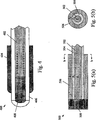
Dementsprechend sind
In einer beispielhaften Ausführungsform könnte es sich bei allen Materialien, die für die Halbleiter S1 bis S4 verwendet werden, um epitaxial aufgebrachte Halbleiter handeln, welche an ihren Grenzflächen Heteroübergänge bilden. Hierdurch könnten die Grenzflächenzustände verringert oder eliminiert werden, welche ein Problem für TFET-Strukturen darstellen, wie der in
Obwohl in der dargestellten beispielhaften Ausführungsform ein konzentrischer kreisförmiger Aufbau für das Kernelement, den Isolator und den äußeren Mantel gezeigt wird, ist abzusehen, dass auch andere geeignete Geometrien benutzt werden können. Zum Beispiel können die Querschnittsformen der einzelnen Elemente andere als kreisförmige sein, z. B. elliptisch, oval, quadratisch oder rechteckig. Ferner ist, obwohl in der dargestellten Ausführungsform Schichten gezeigt werden, die andere Schichten vollständig umgeben (z. B. die Isolatorschicht
Das längliche Kernelement
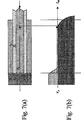
In
Um für S1 und S3 dasselbe Halbleitermaterial zu verwenden, wie oben erwähnt, werden die Dicke von S3 und der Durchmesser von S1 sorgfältig derart eingestellt, dass sich die Energien des Grundzustands so ausrichten, wie in
Zusammengefasst werden durch die IITE-Ausführungsformen die oben beschriebenen Nachteile angegangen. Dies ist schematisch in
Schließlich ist
Die unten angegebenen Ungleichungen gelten sowohl für Elektronen als auch für Defektelektronen, wobei es sich versteht, dass sich die „Energie” für den jeweiligen Fall entweder auf die Elektronen- oder Defektelektronenenergie beziehen kann. Dabei stehen Eb1, Eb2 und Eb3 für Bandkantenenergien (Leitungs- oder Valenzband), E01 und E03 stehen für Grundzustandsenergien der quantisierten Teilbänder, und EF1 und EF3 stehen für die Fermi-Energien der Elektronen- oder Defektelektronen. Das Diagramm
- 1. Die Bandkantenenergie in S2 (Eb2) ist höher als jene in S1 und S3 (Eb1 und Eb3), was bedeutet, dass die Banddiskontinuitäten zwischen S2 und S3 und S1 und S3 positiv sind.
- 2. Die Fermi-Energie in S3 (EF3) ist höher als die Fermi-Energie in S1 (EF1). Hierdurch wird ermöglicht, dass Ladung von S3 nach S1 fließt, wobei diese Bedingung durch die folgende Ungleichung ausgedrückt werden kann:
(EF3 – E03) + (E03 – Eb3) – ΔEb23 > (EF1 – E01) + (E01 – Eb1) – ΔEb21 (Ungl. 1) - 3. Für eine gegebene Bandausrichtung von Eb3 und Eb1 und für gegebene Grundzustandsenergien E01 und E03 muss die Dotierung in S3 hoch genug sein, um EF3 über EF1 zu heben, um die Bedingung 2 zu erfüllen.
- 4. Für eine gegebene Bandausrichtung von Eb3 und Eb1 und für eine gegebene Dotierung in S3 muss der Radius r1 groß genug sein, um E01 zu verringern, und die Radiendifferenz r3 – r2 muss klein genug sein, um E03 zu erhöhen, um die Bedingung 2 zu erfüllen.
- 5. Für die Radien r1 und r2 und für eine gegebene Dotierung in S3 muss die Bandkantenenergie Eb3 in ausreichendem Maße höher sein als Eb1, oder wenn Eb1 höher ist als Eb3, muss die Differenz klein genug sein, um die Bedingung 2 zu Erfüllen. Die Bedingungen für S4 (
7(a) ) sind nicht entscheidend. S4 muss eine ausreichende Dotierung aufweisen oder eine Bandlücke aufweisen, die klein genug ist, um einen guten Ohm'schen Kontakt sowohl mit S1 als auch mit S3 sicherzustellen. S1 und S3 können auch in Nachbarschaft zu S4 dotiert sein, um einen guten Ohm'schen Kontakt sicherzustellen. In diesem Fall kann es sich bei S4 um ein Metall handeln.
- 1. The band edge energy in S2 (E b2 ) is higher than that in S1 and S3 (E b1 and E b3 ), which means that the band discontinuities between S2 and S3 and S1 and S3 are positive.
- 2. The Fermi energy in S3 (E F3 ) is higher than the Fermi energy in S1 (E F1 ). This allows charge to flow from S3 to S1, which condition can be expressed by the following inequality:
(E F3 - E 03 ) + (E 03 - E b3 ) - ΔE b23 > (E F1 - E 01 ) + (E 01 - E b1 ) - ΔE b21 (Unknown 1) - 3. For a given band alignment of E b3 and E b1 and for given ground state energies E 01 and E 03 , the doping in S3 must be high enough to raise E F3 above E F1 to satisfy condition 2.
- 4. For a given band orientation of E b3 and E b1 and for a given doping in S3, the radius r 1 must be large enough to decrease E 01 , and the radius difference r 3 -r 2 must be small enough to be E 03 to raise condition 2.
- 5. For the radii r 1 and r 2 and for a given doping in S3, the band edge energy E b3 must be sufficiently higher than E b1 , or if E b1 is higher than E b3 , the difference must be small enough to be Condition 2 to be fulfilled. The conditions for S4 (
7 (a) ) are not crucial. S4 must have sufficient doping or a bandgap small enough to ensure good ohmic contact with both S1 and S3. S1 and S3 may also be doped adjacent to S4 to ensure good ohmic contact. In this case, S4 may be a metal.
In einer beispielhaften Ausführungsform sind ausgewählte geeignete Halbleitermaterialien die folgenden: InAs0,6P0,2 für S1, InP für S2 und InAs für S3 und S4. Die Radien von S1, S2 und S3 betragen 30 nm, 40 nm bzw. 50 nm. S1 und S4 sind bis zu einer Konzentration von 1019 Atomen/cm3 mit Silicium dotiert, wodurch ein guter Ohm'scher Kontakt von S3 zu S1 über S4 sichergestellt ist und sichergestellt ist, dass die obige Ungl. 1 erfüllt ist. Diese Ungleichung lautet dann wie folgt:
Dies lasst sich wie folgt zusammenfassen:
Somit führt das Einsetzen der ausgewählten Systemparameter in die Terme der Ungleichung zu der Bedingung EF3 > EF1 + 0,0003 eV, welche mit dem gewählten Dotierungsniveau in S3 erfüllt wird. Erneut Bezug nehmend auf
Claims (28)
Applications Claiming Priority (3)
| Application Number | Priority Date | Filing Date | Title |
|---|---|---|---|
| US12/550,857 | 2009-08-31 | ||
| US12/550,857 US8288803B2 (en) | 2009-08-31 | 2009-08-31 | Tunnel field effect devices |
| PCT/IB2010/053884 WO2011024152A1 (en) | 2009-08-31 | 2010-08-30 | Tunnel field effect devices |
Publications (2)
| Publication Number | Publication Date |
|---|---|
| DE112010003495T5 DE112010003495T5 (en) | 2012-09-20 |
| DE112010003495B4 true DE112010003495B4 (en) | 2013-12-12 |
Family
ID=43127353
Family Applications (1)
| Application Number | Title | Priority Date | Filing Date |
|---|---|---|---|
| DE112010003495T Active DE112010003495B4 (en) | 2009-08-31 | 2010-08-30 | Tunnel field effect transistor structure and method of manufacture |
Country Status (7)
| Country | Link |
|---|---|
| US (1) | US8288803B2 (en) |
| JP (1) | JP5501463B2 (en) |
| CN (1) | CN102484132B (en) |
| DE (1) | DE112010003495B4 (en) |
| GB (1) | GB2485495B (en) |
| TW (1) | TWI463653B (en) |
| WO (1) | WO2011024152A1 (en) |
Families Citing this family (11)
| Publication number | Priority date | Publication date | Assignee | Title |
|---|---|---|---|---|
| US8890120B2 (en) | 2012-11-16 | 2014-11-18 | Intel Corporation | Tunneling field effect transistors (TFETs) for CMOS approaches to fabricating N-type and P-type TFETs |
| WO2015047354A1 (en) * | 2013-09-27 | 2015-04-02 | Intel Corporation | Improved cladding layer epitaxy via template engineering for heterogeneous integration on silicon |
| GB2518679A (en) * | 2013-09-30 | 2015-04-01 | Ibm | Reconfigurable tunnel field-effect transistors |
| KR102157825B1 (en) | 2014-01-16 | 2020-09-18 | 삼성전자주식회사 | Tunneling field effect transistor |
| CN104835840B (en) * | 2015-03-24 | 2017-09-19 | 北京大学 | Super steep averagely subthreshold amplitude of oscillation nanowire tunneling field-effect transistor and preparation method |
| US10026830B2 (en) | 2015-04-29 | 2018-07-17 | Stmicroelectronics, Inc. | Tunneling field effect transistor (TFET) having a semiconductor fin structure |
| JP6159777B2 (en) * | 2015-10-28 | 2017-07-05 | ユニサンティス エレクトロニクス シンガポール プライベート リミテッドUnisantis Electronics Singapore Pte Ltd. | Semiconductor device manufacturing method and semiconductor device |
| JP6375316B2 (en) * | 2016-01-06 | 2018-08-15 | ユニサンティス エレクトロニクス シンガポール プライベート リミテッドUnisantis Electronics Singapore Pte Ltd. | Semiconductor device manufacturing method and semiconductor device |
| JP6080989B2 (en) * | 2016-01-06 | 2017-02-15 | ユニサンティス エレクトロニクス シンガポール プライベート リミテッドUnisantis Electronics Singapore Pte Ltd. | Semiconductor device manufacturing method and semiconductor device |
| JP6114434B2 (en) * | 2016-04-21 | 2017-04-12 | ユニサンティス エレクトロニクス シンガポール プライベート リミテッドUnisantis Electronics Singapore Pte Ltd. | Semiconductor device |
| WO2017181404A1 (en) | 2016-04-22 | 2017-10-26 | 华为技术有限公司 | Tunneling field-effect transistor and manufacturing method therefor |
Citations (1)
| Publication number | Priority date | Publication date | Assignee | Title |
|---|---|---|---|---|
| US20080067495A1 (en) * | 2006-09-15 | 2008-03-20 | Interuniversitair Microelektronica Centrum (Imec) | Tunnel effect transistors based on silicon nanowires |
Family Cites Families (7)
| Publication number | Priority date | Publication date | Assignee | Title |
|---|---|---|---|---|
| US6833556B2 (en) * | 2002-08-12 | 2004-12-21 | Acorn Technologies, Inc. | Insulated gate field effect transistor having passivated schottky barriers to the channel |
| US7180107B2 (en) * | 2004-05-25 | 2007-02-20 | International Business Machines Corporation | Method of fabricating a tunneling nanotube field effect transistor |
| US7465976B2 (en) | 2005-05-13 | 2008-12-16 | Intel Corporation | Tunneling field effect transistor using angled implants for forming asymmetric source/drain regions |
| US20070052012A1 (en) * | 2005-08-24 | 2007-03-08 | Micron Technology, Inc. | Vertical tunneling nano-wire transistor |
| EP1901355B1 (en) * | 2006-09-15 | 2015-11-11 | Imec | Tunnel effect transistors based on monocrystalline nanowires having a heterostructure |
| US8120115B2 (en) * | 2007-03-12 | 2012-02-21 | Imec | Tunnel field-effect transistor with gated tunnel barrier |
| US20090034355A1 (en) | 2007-07-30 | 2009-02-05 | Qimonda Ag | Integrated circuit including memory cells with tunnel fet as selection transistor |
-
2009
- 2009-08-31 US US12/550,857 patent/US8288803B2/en active Active
-
2010
- 2010-06-28 TW TW099121078A patent/TWI463653B/en active
- 2010-08-30 CN CN201080038343.7A patent/CN102484132B/en active Active
- 2010-08-30 WO PCT/IB2010/053884 patent/WO2011024152A1/en active Application Filing
- 2010-08-30 JP JP2012526177A patent/JP5501463B2/en not_active Expired - Fee Related
- 2010-08-30 DE DE112010003495T patent/DE112010003495B4/en active Active
- 2010-08-30 GB GB1200880.1A patent/GB2485495B/en not_active Expired - Fee Related
Patent Citations (1)
| Publication number | Priority date | Publication date | Assignee | Title |
|---|---|---|---|---|
| US20080067495A1 (en) * | 2006-09-15 | 2008-03-20 | Interuniversitair Microelektronica Centrum (Imec) | Tunnel effect transistors based on silicon nanowires |
Non-Patent Citations (2)
| Title |
|---|
| Lu, W. et al.: Nanowire Transistor Performance Limits and Applications. In: IEEE Transactions on Electron Devices, 55, 2008, 11, 2859. * |
| Thelander, C. et al.: Nanowire-based one-dimensional electronics. In: materialstoday, 9, 2006, 10, 28. * |
Also Published As
| Publication number | Publication date |
|---|---|
| DE112010003495T5 (en) | 2012-09-20 |
| GB2485495A (en) | 2012-05-16 |
| CN102484132B (en) | 2014-07-30 |
| US8288803B2 (en) | 2012-10-16 |
| GB201200880D0 (en) | 2012-02-29 |
| GB2485495B (en) | 2013-10-30 |
| CN102484132A (en) | 2012-05-30 |
| JP5501463B2 (en) | 2014-05-21 |
| TW201133837A (en) | 2011-10-01 |
| TWI463653B (en) | 2014-12-01 |
| WO2011024152A1 (en) | 2011-03-03 |
| US20110049474A1 (en) | 2011-03-03 |
| JP2013503471A (en) | 2013-01-31 |
Similar Documents
| Publication | Publication Date | Title |
|---|---|---|
| DE112010003495B4 (en) | Tunnel field effect transistor structure and method of manufacture | |
| DE102008000660B4 (en) | The silicon carbide semiconductor device | |
| DE112013001023B4 (en) | Method of fabricating tunnel transistors with abrupt transitions and corresponding tunneling transistors | |
| DE102009031316B4 (en) | Semiconductor device and method for manufacturing a semiconductor device | |
| DE102013003283B4 (en) | Tunneling transistor and method | |
| EP2380201B1 (en) | Unipolar heterojunction depletion-layer transistor | |
| DE112013005369B4 (en) | Gate all-around carbon nanotube transistor with doped spacers | |
| DE102006045214B4 (en) | Semiconductor device with an LDMOS transistor and method of making the same | |
| DE2910566C2 (en) | Static induction semiconductor device | |
| DE102008057412B4 (en) | Semiconductor component, in particular Leistungshalbeiterbauelement | |
| DE102012107523B4 (en) | HEMT with integrated diode with low forward voltage | |
| DE60034328T2 (en) | ELECTROSTATICALLY CONTROLLED TUNNEL EFFECT TRANSISTOR | |
| DE102005046427B4 (en) | Power transistor with parallel nanowires | |
| DE10036208A1 (en) | Current control semiconductor device has current within lateral channel region controlled via at least one depletion zone | |
| DE2619663B2 (en) | Field effect transistor, method of its operation and use as a high-speed switch and in an integrated circuit | |
| DE102014107295B4 (en) | SEMICONDUCTOR DEVICE, METHOD FOR PRODUCING A SEMICONDUCTOR DEVICE AND INTEGRATED CIRCUIT | |
| DE102014108913A1 (en) | Insulated gate bipolar transistor device, semiconductor device and method of forming the devices | |
| DE69724578T2 (en) | The SOI MOS field effect transistor | |
| DE112019002870T5 (en) | Two Gate Conductor Transistors and Related Processes | |
| DE102016207054B4 (en) | field effect transistor | |
| DE102019004795A1 (en) | SHORT CIRCUIT PERFORMANCE FOR SILICON CARBIDE SEMICONDUCTOR DEVICE | |
| DE112013002267T5 (en) | Semiconductor device | |
| DE3411020A1 (en) | IG SEMICONDUCTOR DEVICE WITH LOW ON-RESISTANCE | |
| DE102016117264B4 (en) | Power semiconductor component with controllability of dU / dt | |
| DE112013002260B4 (en) | Manufacturing process of an integrated circuit |
Legal Events
| Date | Code | Title | Description |
|---|---|---|---|
| R163 | Identified publications notified | ||
| R012 | Request for examination validly filed | ||
| R081 | Change of applicant/patentee |
Owner name: GLOBALFOUNDRIES INC., KY Free format text: FORMER OWNER: IBM CORP., ARMONK, N.Y., US |
|
| R082 | Change of representative |
Representative=s name: RICHARDT PATENTANWAELTE PART GMBB, DE Representative=s name: RICHARDT PATENTANWAELTE GBR, DE Representative=s name: RICHARDT PATENTANWAELTE PARTG MBB, DE |
|
| R079 | Amendment of ipc main class |
Free format text: PREVIOUS MAIN CLASS: H01L0029739000 Ipc: H01L0029680000 |
|
| R016 | Response to examination communication | ||
| R016 | Response to examination communication | ||
| R079 | Amendment of ipc main class |
Free format text: PREVIOUS MAIN CLASS: H01L0029739000 Ipc: H01L0029680000 Effective date: 20130527 |
|
| R016 | Response to examination communication | ||
| R018 | Grant decision by examination section/examining division | ||
| R084 | Declaration of willingness to licence | ||
| R020 | Patent grant now final |
Effective date: 20140313 |
|
| R081 | Change of applicant/patentee |
Owner name: GLOBALFOUNDRIES U.S. INC., SANTA CLARA, US Free format text: FORMER OWNER: INTERNATIONAL BUSINESS MACHINES CORPORATION, ARMONK, N.Y., US Owner name: GLOBALFOUNDRIES INC., KY Free format text: FORMER OWNER: INTERNATIONAL BUSINESS MACHINES CORPORATION, ARMONK, N.Y., US |
|
| R082 | Change of representative |
Representative=s name: GRUENECKER PATENT- UND RECHTSANWAELTE PARTG MB, DE Representative=s name: RICHARDT PATENTANWAELTE PARTG MBB, DE |
|
| R081 | Change of applicant/patentee |
Owner name: GLOBALFOUNDRIES U.S. INC., SANTA CLARA, US Free format text: FORMER OWNER: GLOBALFOUNDRIES US 2 LLC (N.D.GES.DES STAATES DELAWARE), HOPEWELL JUNCTION, N.Y., US Owner name: GLOBALFOUNDRIES INC., KY Free format text: FORMER OWNER: GLOBALFOUNDRIES US 2 LLC (N.D.GES.DES STAATES DELAWARE), HOPEWELL JUNCTION, N.Y., US |
|
| R082 | Change of representative |
Representative=s name: GRUENECKER PATENT- UND RECHTSANWAELTE PARTG MB, DE Representative=s name: RICHARDT PATENTANWAELTE PARTG MBB, DE |
|
| R081 | Change of applicant/patentee |
Owner name: GLOBALFOUNDRIES U.S. INC., SANTA CLARA, US Free format text: FORMER OWNER: GLOBALFOUNDRIES INC., GRAND CAYMAN, KY |
|
| R082 | Change of representative |
Representative=s name: GRUENECKER PATENT- UND RECHTSANWAELTE PARTG MB, DE |