DE112010003373T5 - Photocatalytic multi-layer metal compound thin film and process for its production - Google Patents
Photocatalytic multi-layer metal compound thin film and process for its production Download PDFInfo
- Publication number
- DE112010003373T5 DE112010003373T5 DE112010003373T DE112010003373T DE112010003373T5 DE 112010003373 T5 DE112010003373 T5 DE 112010003373T5 DE 112010003373 T DE112010003373 T DE 112010003373T DE 112010003373 T DE112010003373 T DE 112010003373T DE 112010003373 T5 DE112010003373 T5 DE 112010003373T5
- Authority
- DE
- Germany
- Prior art keywords
- thin film
- metal compound
- photocatalytic
- compound thin
- film
- Prior art date
- Legal status (The legal status is an assumption and is not a legal conclusion. Google has not performed a legal analysis and makes no representation as to the accuracy of the status listed.)
- Withdrawn
Links
- 239000010409 thin film Substances 0.000 title claims abstract description 132
- 230000001699 photocatalysis Effects 0.000 title claims abstract description 76
- 150000002736 metal compounds Chemical class 0.000 title claims abstract description 64
- 238000000034 method Methods 0.000 title claims description 59
- 238000004519 manufacturing process Methods 0.000 title abstract description 7
- 239000010408 film Substances 0.000 claims abstract description 55
- 239000000758 substrate Substances 0.000 claims abstract description 48
- 238000004544 sputter deposition Methods 0.000 claims abstract description 31
- GWEVSGVZZGPLCZ-UHFFFAOYSA-N Titan oxide Chemical compound O=[Ti]=O GWEVSGVZZGPLCZ-UHFFFAOYSA-N 0.000 claims abstract description 29
- OGIDPMRJRNCKJF-UHFFFAOYSA-N titanium oxide Inorganic materials [Ti]=O OGIDPMRJRNCKJF-UHFFFAOYSA-N 0.000 claims abstract description 29
- 239000005300 metallic glass Substances 0.000 claims abstract description 11
- 229910052751 metal Inorganic materials 0.000 claims description 8
- 239000002184 metal Substances 0.000 claims description 8
- VYPSYNLAJGMNEJ-UHFFFAOYSA-N Silicium dioxide Chemical compound O=[Si]=O VYPSYNLAJGMNEJ-UHFFFAOYSA-N 0.000 claims description 5
- 229910052814 silicon oxide Inorganic materials 0.000 claims description 5
- 239000000376 reactant Substances 0.000 claims description 4
- 229910052756 noble gas Inorganic materials 0.000 claims description 3
- 238000000151 deposition Methods 0.000 claims 1
- 230000001678 irradiating effect Effects 0.000 claims 1
- 239000011521 glass Substances 0.000 abstract description 18
- 230000015572 biosynthetic process Effects 0.000 abstract description 15
- 238000010438 heat treatment Methods 0.000 abstract description 5
- 239000007789 gas Substances 0.000 description 45
- XKRFYHLGVUSROY-UHFFFAOYSA-N Argon Chemical compound [Ar] XKRFYHLGVUSROY-UHFFFAOYSA-N 0.000 description 34
- 229910010413 TiO 2 Inorganic materials 0.000 description 22
- 238000006243 chemical reaction Methods 0.000 description 21
- 229910052786 argon Inorganic materials 0.000 description 17
- MYMOFIZGZYHOMD-UHFFFAOYSA-N Dioxygen Chemical compound O=O MYMOFIZGZYHOMD-UHFFFAOYSA-N 0.000 description 15
- 229910001882 dioxygen Inorganic materials 0.000 description 15
- 230000000052 comparative effect Effects 0.000 description 12
- 229910004298 SiO 2 Inorganic materials 0.000 description 9
- RTAQQCXQSZGOHL-UHFFFAOYSA-N Titanium Chemical compound [Ti] RTAQQCXQSZGOHL-UHFFFAOYSA-N 0.000 description 8
- 239000010936 titanium Substances 0.000 description 8
- 229910052719 titanium Inorganic materials 0.000 description 8
- 239000003921 oil Substances 0.000 description 6
- XUIMIQQOPSSXEZ-UHFFFAOYSA-N Silicon Chemical compound [Si] XUIMIQQOPSSXEZ-UHFFFAOYSA-N 0.000 description 4
- 239000013078 crystal Substances 0.000 description 4
- 238000011156 evaluation Methods 0.000 description 4
- 238000009832 plasma treatment Methods 0.000 description 4
- 229910052710 silicon Inorganic materials 0.000 description 4
- 239000010703 silicon Substances 0.000 description 4
- 238000012512 characterization method Methods 0.000 description 3
- 239000003795 chemical substances by application Substances 0.000 description 3
- 230000000694 effects Effects 0.000 description 3
- 239000000463 material Substances 0.000 description 3
- 230000005012 migration Effects 0.000 description 3
- 238000013508 migration Methods 0.000 description 3
- 238000005192 partition Methods 0.000 description 3
- 239000002994 raw material Substances 0.000 description 3
- XLYOFNOQVPJJNP-UHFFFAOYSA-N water Substances O XLYOFNOQVPJJNP-UHFFFAOYSA-N 0.000 description 3
- 150000001875 compounds Chemical class 0.000 description 2
- 238000010586 diagram Methods 0.000 description 2
- 239000001301 oxygen Substances 0.000 description 2
- 229910052760 oxygen Inorganic materials 0.000 description 2
- 230000001105 regulatory effect Effects 0.000 description 2
- 238000005477 sputtering target Methods 0.000 description 2
- 150000003609 titanium compounds Chemical class 0.000 description 2
- 238000009281 ultraviolet germicidal irradiation Methods 0.000 description 2
- 238000002441 X-ray diffraction Methods 0.000 description 1
- 230000004913 activation Effects 0.000 description 1
- 230000000844 anti-bacterial effect Effects 0.000 description 1
- QVGXLLKOCUKJST-UHFFFAOYSA-N atomic oxygen Chemical compound [O] QVGXLLKOCUKJST-UHFFFAOYSA-N 0.000 description 1
- 230000005540 biological transmission Effects 0.000 description 1
- 239000004566 building material Substances 0.000 description 1
- 230000015556 catabolic process Effects 0.000 description 1
- 230000003197 catalytic effect Effects 0.000 description 1
- 239000000919 ceramic Substances 0.000 description 1
- 238000007796 conventional method Methods 0.000 description 1
- 238000006731 degradation reaction Methods 0.000 description 1
- 230000001877 deodorizing effect Effects 0.000 description 1
- 238000002524 electron diffraction data Methods 0.000 description 1
- 238000001704 evaporation Methods 0.000 description 1
- 238000001755 magnetron sputter deposition Methods 0.000 description 1
- 229910044991 metal oxide Inorganic materials 0.000 description 1
- 150000004706 metal oxides Chemical class 0.000 description 1
- 239000013081 microcrystal Substances 0.000 description 1
- -1 oxygen ion Chemical class 0.000 description 1
- 230000002093 peripheral effect Effects 0.000 description 1
- 239000002243 precursor Substances 0.000 description 1
- 238000002360 preparation method Methods 0.000 description 1
- 230000001681 protective effect Effects 0.000 description 1
- 238000005546 reactive sputtering Methods 0.000 description 1
- 239000011347 resin Substances 0.000 description 1
- 229920005989 resin Polymers 0.000 description 1
Images


Classifications
-
- C—CHEMISTRY; METALLURGY
- C23—COATING METALLIC MATERIAL; COATING MATERIAL WITH METALLIC MATERIAL; CHEMICAL SURFACE TREATMENT; DIFFUSION TREATMENT OF METALLIC MATERIAL; COATING BY VACUUM EVAPORATION, BY SPUTTERING, BY ION IMPLANTATION OR BY CHEMICAL VAPOUR DEPOSITION, IN GENERAL; INHIBITING CORROSION OF METALLIC MATERIAL OR INCRUSTATION IN GENERAL
- C23C—COATING METALLIC MATERIAL; COATING MATERIAL WITH METALLIC MATERIAL; SURFACE TREATMENT OF METALLIC MATERIAL BY DIFFUSION INTO THE SURFACE, BY CHEMICAL CONVERSION OR SUBSTITUTION; COATING BY VACUUM EVAPORATION, BY SPUTTERING, BY ION IMPLANTATION OR BY CHEMICAL VAPOUR DEPOSITION, IN GENERAL
- C23C14/00—Coating by vacuum evaporation, by sputtering or by ion implantation of the coating forming material
- C23C14/22—Coating by vacuum evaporation, by sputtering or by ion implantation of the coating forming material characterised by the process of coating
- C23C14/34—Sputtering
-
- B—PERFORMING OPERATIONS; TRANSPORTING
- B01—PHYSICAL OR CHEMICAL PROCESSES OR APPARATUS IN GENERAL
- B01J—CHEMICAL OR PHYSICAL PROCESSES, e.g. CATALYSIS OR COLLOID CHEMISTRY; THEIR RELEVANT APPARATUS
- B01J21/00—Catalysts comprising the elements, oxides, or hydroxides of magnesium, boron, aluminium, carbon, silicon, titanium, zirconium, or hafnium
- B01J21/06—Silicon, titanium, zirconium or hafnium; Oxides or hydroxides thereof
- B01J21/063—Titanium; Oxides or hydroxides thereof
-
- B—PERFORMING OPERATIONS; TRANSPORTING
- B01—PHYSICAL OR CHEMICAL PROCESSES OR APPARATUS IN GENERAL
- B01D—SEPARATION
- B01D53/00—Separation of gases or vapours; Recovering vapours of volatile solvents from gases; Chemical or biological purification of waste gases, e.g. engine exhaust gases, smoke, fumes, flue gases, aerosols
- B01D53/34—Chemical or biological purification of waste gases
- B01D53/74—General processes for purification of waste gases; Apparatus or devices specially adapted therefor
- B01D53/86—Catalytic processes
- B01D53/8678—Removing components of undefined structure
- B01D53/8687—Organic components
-
- B—PERFORMING OPERATIONS; TRANSPORTING
- B01—PHYSICAL OR CHEMICAL PROCESSES OR APPARATUS IN GENERAL
- B01J—CHEMICAL OR PHYSICAL PROCESSES, e.g. CATALYSIS OR COLLOID CHEMISTRY; THEIR RELEVANT APPARATUS
- B01J21/00—Catalysts comprising the elements, oxides, or hydroxides of magnesium, boron, aluminium, carbon, silicon, titanium, zirconium, or hafnium
- B01J21/06—Silicon, titanium, zirconium or hafnium; Oxides or hydroxides thereof
-
- B01J35/39—
-
- B—PERFORMING OPERATIONS; TRANSPORTING
- B01—PHYSICAL OR CHEMICAL PROCESSES OR APPARATUS IN GENERAL
- B01J—CHEMICAL OR PHYSICAL PROCESSES, e.g. CATALYSIS OR COLLOID CHEMISTRY; THEIR RELEVANT APPARATUS
- B01J37/00—Processes, in general, for preparing catalysts; Processes, in general, for activation of catalysts
- B01J37/02—Impregnation, coating or precipitation
- B01J37/0215—Coating
- B01J37/0217—Pretreatment of the substrate before coating
-
- B—PERFORMING OPERATIONS; TRANSPORTING
- B01—PHYSICAL OR CHEMICAL PROCESSES OR APPARATUS IN GENERAL
- B01J—CHEMICAL OR PHYSICAL PROCESSES, e.g. CATALYSIS OR COLLOID CHEMISTRY; THEIR RELEVANT APPARATUS
- B01J37/00—Processes, in general, for preparing catalysts; Processes, in general, for activation of catalysts
- B01J37/02—Impregnation, coating or precipitation
- B01J37/024—Multiple impregnation or coating
- B01J37/0244—Coatings comprising several layers
-
- B—PERFORMING OPERATIONS; TRANSPORTING
- B01—PHYSICAL OR CHEMICAL PROCESSES OR APPARATUS IN GENERAL
- B01J—CHEMICAL OR PHYSICAL PROCESSES, e.g. CATALYSIS OR COLLOID CHEMISTRY; THEIR RELEVANT APPARATUS
- B01J37/00—Processes, in general, for preparing catalysts; Processes, in general, for activation of catalysts
- B01J37/34—Irradiation by, or application of, electric, magnetic or wave energy, e.g. ultrasonic waves ; Ionic sputtering; Flame or plasma spraying; Particle radiation
- B01J37/341—Irradiation by, or application of, electric, magnetic or wave energy, e.g. ultrasonic waves ; Ionic sputtering; Flame or plasma spraying; Particle radiation making use of electric or magnetic fields, wave energy or particle radiation
- B01J37/347—Ionic or cathodic spraying; Electric discharge
-
- C—CHEMISTRY; METALLURGY
- C01—INORGANIC CHEMISTRY
- C01G—COMPOUNDS CONTAINING METALS NOT COVERED BY SUBCLASSES C01D OR C01F
- C01G23/00—Compounds of titanium
- C01G23/04—Oxides; Hydroxides
-
- C—CHEMISTRY; METALLURGY
- C03—GLASS; MINERAL OR SLAG WOOL
- C03C—CHEMICAL COMPOSITION OF GLASSES, GLAZES OR VITREOUS ENAMELS; SURFACE TREATMENT OF GLASS; SURFACE TREATMENT OF FIBRES OR FILAMENTS MADE FROM GLASS, MINERALS OR SLAGS; JOINING GLASS TO GLASS OR OTHER MATERIALS
- C03C17/00—Surface treatment of glass, not in the form of fibres or filaments, by coating
- C03C17/34—Surface treatment of glass, not in the form of fibres or filaments, by coating with at least two coatings having different compositions
- C03C17/36—Surface treatment of glass, not in the form of fibres or filaments, by coating with at least two coatings having different compositions at least one coating being a metal
- C03C17/3602—Surface treatment of glass, not in the form of fibres or filaments, by coating with at least two coatings having different compositions at least one coating being a metal the metal being present as a layer
- C03C17/3607—Coatings of the type glass/inorganic compound/metal
-
- C—CHEMISTRY; METALLURGY
- C23—COATING METALLIC MATERIAL; COATING MATERIAL WITH METALLIC MATERIAL; CHEMICAL SURFACE TREATMENT; DIFFUSION TREATMENT OF METALLIC MATERIAL; COATING BY VACUUM EVAPORATION, BY SPUTTERING, BY ION IMPLANTATION OR BY CHEMICAL VAPOUR DEPOSITION, IN GENERAL; INHIBITING CORROSION OF METALLIC MATERIAL OR INCRUSTATION IN GENERAL
- C23C—COATING METALLIC MATERIAL; COATING MATERIAL WITH METALLIC MATERIAL; SURFACE TREATMENT OF METALLIC MATERIAL BY DIFFUSION INTO THE SURFACE, BY CHEMICAL CONVERSION OR SUBSTITUTION; COATING BY VACUUM EVAPORATION, BY SPUTTERING, BY ION IMPLANTATION OR BY CHEMICAL VAPOUR DEPOSITION, IN GENERAL
- C23C14/00—Coating by vacuum evaporation, by sputtering or by ion implantation of the coating forming material
- C23C14/0021—Reactive sputtering or evaporation
- C23C14/0036—Reactive sputtering
-
- C—CHEMISTRY; METALLURGY
- C23—COATING METALLIC MATERIAL; COATING MATERIAL WITH METALLIC MATERIAL; CHEMICAL SURFACE TREATMENT; DIFFUSION TREATMENT OF METALLIC MATERIAL; COATING BY VACUUM EVAPORATION, BY SPUTTERING, BY ION IMPLANTATION OR BY CHEMICAL VAPOUR DEPOSITION, IN GENERAL; INHIBITING CORROSION OF METALLIC MATERIAL OR INCRUSTATION IN GENERAL
- C23C—COATING METALLIC MATERIAL; COATING MATERIAL WITH METALLIC MATERIAL; SURFACE TREATMENT OF METALLIC MATERIAL BY DIFFUSION INTO THE SURFACE, BY CHEMICAL CONVERSION OR SUBSTITUTION; COATING BY VACUUM EVAPORATION, BY SPUTTERING, BY ION IMPLANTATION OR BY CHEMICAL VAPOUR DEPOSITION, IN GENERAL
- C23C14/00—Coating by vacuum evaporation, by sputtering or by ion implantation of the coating forming material
- C23C14/06—Coating by vacuum evaporation, by sputtering or by ion implantation of the coating forming material characterised by the coating material
- C23C14/08—Oxides
- C23C14/083—Oxides of refractory metals or yttrium
-
- C—CHEMISTRY; METALLURGY
- C23—COATING METALLIC MATERIAL; COATING MATERIAL WITH METALLIC MATERIAL; CHEMICAL SURFACE TREATMENT; DIFFUSION TREATMENT OF METALLIC MATERIAL; COATING BY VACUUM EVAPORATION, BY SPUTTERING, BY ION IMPLANTATION OR BY CHEMICAL VAPOUR DEPOSITION, IN GENERAL; INHIBITING CORROSION OF METALLIC MATERIAL OR INCRUSTATION IN GENERAL
- C23C—COATING METALLIC MATERIAL; COATING MATERIAL WITH METALLIC MATERIAL; SURFACE TREATMENT OF METALLIC MATERIAL BY DIFFUSION INTO THE SURFACE, BY CHEMICAL CONVERSION OR SUBSTITUTION; COATING BY VACUUM EVAPORATION, BY SPUTTERING, BY ION IMPLANTATION OR BY CHEMICAL VAPOUR DEPOSITION, IN GENERAL
- C23C14/00—Coating by vacuum evaporation, by sputtering or by ion implantation of the coating forming material
- C23C14/06—Coating by vacuum evaporation, by sputtering or by ion implantation of the coating forming material characterised by the coating material
- C23C14/10—Glass or silica
-
- C—CHEMISTRY; METALLURGY
- C23—COATING METALLIC MATERIAL; COATING MATERIAL WITH METALLIC MATERIAL; CHEMICAL SURFACE TREATMENT; DIFFUSION TREATMENT OF METALLIC MATERIAL; COATING BY VACUUM EVAPORATION, BY SPUTTERING, BY ION IMPLANTATION OR BY CHEMICAL VAPOUR DEPOSITION, IN GENERAL; INHIBITING CORROSION OF METALLIC MATERIAL OR INCRUSTATION IN GENERAL
- C23C—COATING METALLIC MATERIAL; COATING MATERIAL WITH METALLIC MATERIAL; SURFACE TREATMENT OF METALLIC MATERIAL BY DIFFUSION INTO THE SURFACE, BY CHEMICAL CONVERSION OR SUBSTITUTION; COATING BY VACUUM EVAPORATION, BY SPUTTERING, BY ION IMPLANTATION OR BY CHEMICAL VAPOUR DEPOSITION, IN GENERAL
- C23C14/00—Coating by vacuum evaporation, by sputtering or by ion implantation of the coating forming material
- C23C14/22—Coating by vacuum evaporation, by sputtering or by ion implantation of the coating forming material characterised by the process of coating
- C23C14/34—Sputtering
- C23C14/35—Sputtering by application of a magnetic field, e.g. magnetron sputtering
- C23C14/352—Sputtering by application of a magnetic field, e.g. magnetron sputtering using more than one target
-
- B—PERFORMING OPERATIONS; TRANSPORTING
- B01—PHYSICAL OR CHEMICAL PROCESSES OR APPARATUS IN GENERAL
- B01D—SEPARATION
- B01D2255/00—Catalysts
- B01D2255/20—Metals or compounds thereof
- B01D2255/207—Transition metals
- B01D2255/20707—Titanium
-
- B—PERFORMING OPERATIONS; TRANSPORTING
- B01—PHYSICAL OR CHEMICAL PROCESSES OR APPARATUS IN GENERAL
- B01D—SEPARATION
- B01D2255/00—Catalysts
- B01D2255/30—Silica
-
- B—PERFORMING OPERATIONS; TRANSPORTING
- B01—PHYSICAL OR CHEMICAL PROCESSES OR APPARATUS IN GENERAL
- B01D—SEPARATION
- B01D2255/00—Catalysts
- B01D2255/80—Type of catalytic reaction
- B01D2255/802—Photocatalytic
-
- B—PERFORMING OPERATIONS; TRANSPORTING
- B01—PHYSICAL OR CHEMICAL PROCESSES OR APPARATUS IN GENERAL
- B01D—SEPARATION
- B01D2255/00—Catalysts
- B01D2255/90—Physical characteristics of catalysts
- B01D2255/902—Multilayered catalyst
- B01D2255/9025—Three layers
-
- C—CHEMISTRY; METALLURGY
- C03—GLASS; MINERAL OR SLAG WOOL
- C03C—CHEMICAL COMPOSITION OF GLASSES, GLAZES OR VITREOUS ENAMELS; SURFACE TREATMENT OF GLASS; SURFACE TREATMENT OF FIBRES OR FILAMENTS MADE FROM GLASS, MINERALS OR SLAGS; JOINING GLASS TO GLASS OR OTHER MATERIALS
- C03C2217/00—Coatings on glass
- C03C2217/70—Properties of coatings
- C03C2217/71—Photocatalytic coatings
Abstract
Aufgabe: Schnelles und billiges Bereitstellen eines photokatalytischen Titanoxid-Dünnfilms, der hohe photokatalytische Eigenschaften aufweist, bei einer niedrigen Temperatur. Mittel zur Lösung: Der Dünnfilm umfasst eine Keimschicht aus einem amorphen Metallverbindungs-Dünnfilm, die an der Oberfläche eines Substrats wie etwa Glas oder Kunststoff gebildet wurde, und einen kristallinen Metallverbindungs-Dünnfilm, der säulenförmig gezüchtet auf der Keimschicht gebildet wurde. Bei der Herstellung des Dünnfilms wird keine Vorbehandlung oder Nachbehandlung durch ein Plasma eines reaktiven Gases mittels eines Sputterverfahrens und auch keine Erhitzungsbehandlung vorgenommen, weshalb der photokatalytische Titanoxid-Dünnfilm durch eine schnelle Filmbildung bei einer niedrigen Temperatur billig hergestellt wird.Task: Rapid and cheap provision of a photocatalytic titanium oxide thin film, which has high photocatalytic properties, at a low temperature. Means for solving: The thin film comprises a seed layer of an amorphous metal compound thin film formed on the surface of a substrate such as glass or plastic, and a crystalline metal compound thin film formed in a columnar shape grown on the seed layer. In the production of the thin film, no pretreatment or post-treatment by a plasma of a reactive gas by means of a sputtering method nor heat treatment is performed, and therefore the photocatalytic titanium oxide thin film is cheaply made by rapid film formation at a low temperature.
Description
Bezeichnung der Erfindung: Photokatalytischer mehrschichtiger Metallverbindungs-Dünnfilm und Verfahren zu seiner HerstellungDescription of the Invention: Photocatalytic multilayer metal compound thin film and method of making the same
Technisches GebietTechnical area
Die vorliegende Erfindung betrifft einen photokatalytischen Metallverbindungs-Dünnfilm, und betrifft insbesondere einen photokatalytischen mehrschichtigen Metallverbindungs-Dünnfilm, der eine Kristallstruktur aufweist, die durch eine Filmbildung mit einer hohen Geschwindigkeit und unter niedrigen Temperaturbedingungen gebildet wird, sowie ein Verfahren zu seiner Herstellung.The present invention relates to a photocatalytic metal compound thin film, and more particularly to a photocatalytic multilayer metal compound thin film having a crystal structure formed by film formation at a high speed and under low temperature conditions, and a method for producing the same.
Allgemeiner Stand der TechnikGeneral state of the art
Titanoxidfilme weisen eine photokatalytische Wirkung auf und zeigen herausragende Fähigkeiten wie etwa eine antibakterielle Wirkung, eine desodorierende Wirkung, eine schmutzabweisende Wirkung und Hydrophilizität, und im Besonderen werden hydrophile Dünnfilme verbreitet etwa für Seitenspiegel von Kraftfahrzeugen, Spiegel, die an Straßen eingerichtet sind, oder Baumaterialien für Außenwände von Gebäuden verwendet.Titanium oxide films have a photocatalytic action and exhibit excellent abilities such as antibacterial action, deodorizing effect, antisoiling effect and hydrophilicity, and in particular, hydrophilic thin films are widely used for, for example, side mirrors of automobiles, mirrors installed on roads, or building materials for Exterior walls of buildings used.
Da bei einer Anwendung von Titanoxid als photokatalytisches Material normalerweise eine Verwendung erforderlich ist, bei der es in der Form eines Dünnfilms an der Oberfläche irgendeines Substrats fixiert ist, wird eine Sputtertechnik eingesetzt, die es stark an die Oberfläche dieses Substrats heftet. Als herkömmliche Sputtertechnik wird hauptsächlich das reaktive Sputtern eingesetzt, wobei ein Target aus metallischem Titan verwendet wird, Argongas und Sauerstoffgas eingeleitet werden und ein Titanoxid-Dünnfilm gebildet wird. Doch bei diesem Filmbildungsverfahren ist die Filmbildungsgeschwindigkeit mit etwa 10 nm/min langsam und ist überdies zur Hervorbringung der photokatalytischen Wirkung eine Erhitzungsbehandlung des Substrats wie etwa eine Vorbehandlung oder eine Nachbehandlung erforderlich. Es ist zwar auch möglich, einen Titanoxid-Dünnfilm, der eine photokatalytische Wirkung hervorbringt, bei einer niedrigen Temperatur zu bilden, doch ist die Geschwindigkeit äußerst gering, weshalb keine industrielle Verwendung möglich ist.Since an application of titanium oxide as a photocatalytic material usually requires a use of being fixed in the form of a thin film on the surface of any substrate, a sputtering technique is employed which strongly bonds it to the surface of this substrate. As a conventional sputtering technique, mainly reactive sputtering is employed, using a target of metallic titanium, introducing argon gas and oxygen gas, and forming a titanium oxide thin film. However, in this film-forming method, the film-forming speed is slow at about 10 nm / min, and moreover, to bring about the photocatalytic action, a heating treatment of the substrate such as pretreatment or aftertreatment is required. Although it is also possible to form a titanium oxide thin film which brings about a photocatalytic effect at a low temperature, the speed is extremely low, and therefore, no industrial use is possible.
Es wurde eine Technik zur Bildung eines hydrophilen Dünnfilms vorgeschlagen, wobei bei einem Sputterprozess in einem Filmbildungsprozessbereich in einem Vakuumbehälter ein Target aus zumindest einer Art von Metall auf ein Substrat gesputtert wird und ein Filmausgangsmaterial aus dem Metall auf die Oberfläche des Substrats aufgebracht wird, dieses Substrat in einem Substrattransportprozess in einen Reaktionsprozessbereich, der an einer Stelle gebildet ist, die in dem Vakuumbehälter von dem Filmbildungsprozessbereich entfernt ist, transportiert wird, und unter Einleitung zumindest einer Art von reaktivem Gas in den Reaktionsprozessbereich ein Plasma des reaktiven Gases erzeugt wird, das reaktive Gas und das Filmausgangsmaterial reagiert werden, und eine Verbindung oder eine unvollständige Verbindung des reaktiven Gases und des Filmausgangsmaterials gebildet wird (siehe Patentliteraturbeispiel 1).A technique for forming a hydrophilic thin film has been proposed wherein, in a sputtering process in a film forming process area in a vacuum vessel, a target of at least one kind of metal is sputtered on a substrate and a film raw material of the metal is applied to the surface of the substrate, this substrate in a substrate transport process, into a reaction process area formed at a location remote in the vacuum vessel from the film forming process area, and generating a reactive gas plasma by introducing at least one kind of reactive gas into the reaction process area and the film raw material is reacted, and a compound or incomplete compound of the reactive gas and the film raw material is formed (see Patent Literature Example 1).
Literatur der VorläufertechnikLiterature of the precursor technique
PatentliteraturbeispielePatent literature examples
- Patentliteraturbeispiel 1: Patentoffenlegungsschrift 2007-314835Patent Literature Example 1: Patent Publication 2007-314835
-
Nichtpatentliteraturbeispiel 1:
„Thickness depencence of TiO2 films deposited by Oxygen ion assisted reactive evaporation method”, Shôhei MOCHIZUKI; Tetsuya KAGAMI; Taiki ISHIHARA; Noriyuki SATÔ; Kôji, KOBAYASHI; Takeshi MAEDA; Yôichi HOSHI: wissenschaftliche Vorträge bei der 69. Konferenz für Angewandte Physik, 3a-J-8 (September 2008) "Thickness depencence of TiO 2 films deposited by oxygen ion assisted reactive evaporation method", Shôhei MOCHIZUKI; Tetsuya KAGAMI; Taiki ISHIHARA; Noriyuki SATÔ; Kôji, KOBAYASHI; Takeshi MAEDA; Yôichi HOSHI: Scientific Lectures at the 69th Conference on Applied Physics, 3a-J-8 (September 2008)
Kurzdarstellung der ErfindungBrief description of the invention
Aufgabe, die die Erfindung lösen sollTask to solve the invention
Doch bei der Technik zur Herstellung des in dem obigen Patentliteraturbeispiel beschriebenen hydrophilen Dünnfilms besteht das Problem, dass zumindest vor oder nach der Bildung des hydrophilen Dünnfilms an der Oberfläche des Substrats eine Plasmabehandlung durch ein Plasma des reaktiven Gases vorgenommen werden muss, das Substrat durch die Plasmaenergie für eine lange Zeit erhitzt wird und die Bildung eines photokatalytischen Films bei einer niedrigen Temperatur (höchstens 100°C) nicht möglich ist. Außerdem sind für die Dicke des hydrophilen Dünnfilms mindestens 240 nm oder mehr erforderlich, wodurch die Kosten hoch werden.However, in the technique of manufacturing the hydrophilic thin film described in the above Patent Literature, there is a problem that at least before or after the formation of the hydrophilic thin film on the surface of the substrate, a plasma treatment must be performed by a plasma of the reactive gas, the substrate by the plasma energy is heated for a long time and the formation of a photocatalytic film at a low temperature (at most 100 ° C) is not possible. In addition, at least 240 nm or more is required for the thickness of the hydrophilic thin film, whereby the cost becomes high.
Die vorliegende Erfindung erfolgte angesichts der obigen Umstände und stellt bei einer niedrigen Temperatur (höchstens 100°C) ohne jegliche Vornahme einer Vorbehandlung wie etwa einer Plasmabehandlung, die an der Oberfläche des Substrats vorgenommen wird, oder einer Nachbehandlung nach der Bildung des hydrophilen Dünnfilms oder einer Erhitzungsbehandlung schnell und billig einen photokatalytischen mehrschichtigen Metallverbindungs-Dünnfilm mit hohen photokatalytischen Eigenschaften sowie ein Verfahren zu seiner Herstellung bereit.The present invention has been made in view of the above circumstances and provides at a low temperature (at most 100 ° C) without any pretreatment such as a plasma treatment performed on the surface of the substrate or post-treatment after formation of the hydrophilic thin film or film Heat treatment quickly and cheaply a photocatalytic multilayer metal compound thin film with high photocatalytic properties and a method for its preparation ready.
Mittel zur Lösung der Aufgabe Means of solving the task
Zu diesem Zweck besteht die erste Kennzeichnung darin, dass der photokatalytische mehrschichtige Metallverbindungs-Dünnfilm der vorliegenden Erfindung eine an der Oberfläche des Substrats gebildete Keimschicht aus einem Dünnfilm einer amorphen Metallverbindung und einen Dünnfilm einer kristallinen Metallverbindung, der auf der Keimschicht zu einer Säulenform gezüchtet gebildet wurde, umfasst.For this purpose, the first characterization is that the photocatalytic multilayer metal compound thin film of the present invention has formed a seed layer of an amorphous metal compound thin film formed on the surface of the substrate and a crystalline metal compound thin film grown on the seed layer in a columnar form , includes.
Die zweite Kennzeichnung besteht darin, dass die gesamte Dicke der Keimschicht aus dem amorphen Metallverbindungs-Dünnfilm, der an der Oberfläche des Substrats gebildet wurde, und des kristallinen Metallverbindungs-Dünnfilms, der auf der Keimschicht gebildet wurde, mindestens 100 nm oder mehr beträgt.The second mark is that the total thickness of the seed layer made of the amorphous metal compound thin film formed on the surface of the substrate and the crystalline metal compound thin film formed on the seed layer is at least 100 nm or more.
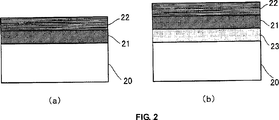
Die dritte Kennzeichnung besteht darin, dass zwischen dem Substrat und der Keimschicht ferner ein Siliziumoxid-Dünnfilm ausgebildet wurde.The third characterization is that a silicon oxide thin film is further formed between the substrate and the seed layer.
Die vierte Kennzeichnung besteht darin, dass bei dem Verfahren zur Herstellung eines photokatalytischen mehrschichtigen Metallverbindungs-Dünnfilms durch Wiederholen eines Prozesses, bei dem durch ein Sputterverfahren an der Oberfläche eines Substrats ein äußerst dünner Film einer Metallverbindung abgelagert wird und eine Bestrahlung mit einer aktivierten Spezies eines Edelgases und eines reaktiven Gases erfolgt, eine Keimschicht aus einem amorphen Metallverbindungs-Dünnfilm gebildet wird, und durch Wiederholen eines Prozesses, bei dem durch ein Sputterverfahren auf dem Keimfilm ein äußerst dünner Film eines Metalls und eines unvollständigen Reaktants des Metalls gebildet wird und eine Bestrahlung mit einer aktivierten Spezies eines Edelgases und eines reaktiven Gases erfolgt, auf der Keimschicht ein kristalliner Metallverbindungs-Dünnfilm zu einer Säulenform gezüchtet gebildet wird.The fourth characterization is that in the method of producing a photocatalytic multilayer metal compound thin film by repeating a process in which a super-thin film of a metal compound is deposited by sputtering on the surface of a substrate and irradiation with an activated species of noble gas and a reactive gas, a seed layer is formed of an amorphous metal compound thin film, and by repeating a process in which an extremely thin film of a metal and an incomplete reactant of the metal is formed by a sputtering process on the seed film, and irradiation with a activated species of a rare gas and a reactive gas is formed on the seed layer is formed a crystalline metal compound thin film grown in a columnar shape.
Die fünfte Kennzeichnung besteht darin, dass der amorphe Metallverbindungs-Dünnfilm und der kristalline Metallverbindungs-Dünnfilm durch Titanoxid gebildet sind. Als Substrat wird wirksam ein Glassubstrat oder ein Keramiksubstrat oder ein Kunststoffsubstrat verwendet.The fifth mark is that the amorphous metal compound thin film and the crystalline metal compound thin film are formed by titanium oxide. As the substrate, a glass substrate or a ceramic substrate or a plastic substrate is effectively used.
Resultat der ErfindungResult of the invention
Da gemäß dem photokatalytischen mehrschichtigen Metallverbindungs-Dünnfilm und dem Verfahren zu seiner Herstellung keine Plasmabehandlung des Substrats durch ein reaktives Gas und keine Erhitzungsbehandlung vorgenommen wird, besteht die herausragende Wirkung, dass ein photokatalytischer Dünnfilm mit hohen katalytischen Eigenschaften bei einer niedrigen Temperatur gebildet werden kann.Since no plasma treatment of the substrate by a reactive gas and no heating treatment is performed according to the photocatalytic multilayer metal compound thin film and the method for its production, there is an excellent effect that a photocatalytic thin film having high catalytic properties can be formed at a low temperature.
Zudem besteht die herausragende Wirkung dass der Film billig ist, da die gesamte Dicke der Keimschicht aus dem amorphen Metallverbindungs-Dünnfilm, der an Oberfläche des Substrats gebildet wurde, und des auf der Keimschicht gebildeten kristallinen Metallverbindungs-Dünnfilms 100 nm oder mehr beträgt und dadurch die Hydrophilizität und die Ölabbaufähigkeit verglichen mit einem bisherigen photokatalytischen Dünnfilm bei einer weniger als halb so dicken Filmdicke in einer kurzen Zeit erreicht werden können und überdies eine Filmbildung mit einer hohen Geschwindigkeit möglich ist.In addition, since the entire thickness of the seed layer made of the amorphous metal compound thin film formed on the surface of the substrate and the crystalline metal compound thin film formed on the seed layer is 100 nm or more, and thereby the Hydrophilicity and oil-degradability can be achieved in a short time compared with a conventional photocatalytic thin film at a film thickness less than half as thick and, moreover, film formation at a high speed is possible.
Einfache Erklärung der ZeichnungenSimple explanation of the drawings
Ausführungsweisen der Erfindung Embodiments of the invention
Nachstehend werden die besten Ausführungsweisen der vorliegenden Erfindung anhand von Ausführungsformen, die in den Zeichnungen gezeigt sind, erklärt, doch muss nicht betont werden, dass keine Beschränkung auf die vorliegenden Ausführungsformen besteht.
Bei der vorliegenden Ausführungsform erfolgt die Erklärung anhand eines Beispiels, bei dem eine Magnetron-Sputtervorrichtung, die zwei Arten von Metalltargets verwendet, als Sputtervorrichtung verwendet wird, doch sind auch andere Vorrichtungen möglich. Als Metall, das für den photokatalytischen Metallverbindungs-Dünnfilm verwendet wird, wird metallisches Titan verwendet.In the present embodiment, explanation will be made by way of an example in which a magnetron sputtering apparatus using two kinds of metal targets is used as the sputtering apparatus, but other apparatuses are possible. As the metal used for the photocatalytic metal compound thin film, metallic titanium is used.
Zwischen den Sputtermitteln
An der äußeren Umfangsfläche der Rotationstrommel
An den Mitteln
Die aus dem oben beschriebenen Aufbau bestehende Sputtervorrichtung
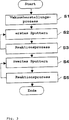
Als nächstes wird anhand von
Erste Ausführungsweise First execution
Zuerst werden Glassubstrate
Dann wird von den Mitteln
Bei diesem Prozess ist in dem Filmbildungsprozessbereich
Wenn die an der Rotationstrommel
Die obigen Schritte S2 und S3 werden durch die Drehung der Rotationstrommel
Als nächstes werden die Durchflussmengen des in die Filmbildungsprozessbereiche
Bei diesem Prozess wird in dem Filmbildungsprozessbereich
Wenn die an der Rotationstrommel
Die obigen Schritte S4 und S5 werden durch die Drehung der Rotationstrommel
Zweite AusführungsweiseSecond embodiment
Als nächstes wird anhand von
Zuerst werden so wie bei der ersten Ausführungsform Glassubstrate
Dann wird von den Mitteln
Bei diesem Prozess ist in dem Filmbildungsprozessbereich
Wenn die an der Rotationstrommel
Die obigen Schritts S21 und S31 werden durch die Drehung der Rotationstrommel
Ausführungsformembodiment
Als nächstes wird das Verfahren zur Herstellung des photokatalytischen mehrschichtigen Metallverbindungs-Dünnfilms der vorliegenden Erfindung anhand einer Ausführungsform, bei der tatsächlich ein photokatalytischer mehrschichtiger Metallverbindungs-Dünnfilm gebildet wurde, erklärt. Die vorliegende Ausführungsform entspricht der oben beschriebenen zweiten Ausführungsweise.Next, the method for producing the photocatalytic multilayer metal compound thin film of the present invention will be explained by an embodiment in which a photocatalytic multilayer metal compound thin film has actually been formed. The present embodiment corresponds to the second embodiment described above.
Unter Verwendung der in
Bedingungen bei der SiO2-Filmbildung: Anlegestrom an das Target: 6,5 kW; Anlegestrom an die Vorrichtung
Conditions for SiO 2 Film Formation: Applying Current to the Target: 6.5 kW; Anleggestrom the
Bedingungen bei der Filmbildung der TiO2-Keimschicht: Anlegestrom an das Target: 3,8 kW; Anlegestrom an die Vorrichtung
Bedingungen bei der Filmbildung der photokatalytischen TiO2-Schicht: Anlegestrom an das Target: 3,0 kW; Anlegestrom an die Vorrichtung
Vergleichsform 1
Unter Verwendung der in
Vergleichsform 2
Unter Verwendung der in
Vergleich der TitanoxidfilmeComparison of titanium oxide films
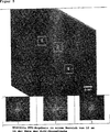
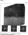
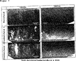
Die Ergebnisse einer Betrachtung der auf dem Glassubstrat gebildeten SiO2/TiO2-Filme von der Schnittflächenrichtung her mit einem Transmissions-Elektronenmikroskop (JEM-4000EM von der JEOL Ltd.) sind in
Vergleich der KristallstrukturComparison of the crystal structure
Bei einem Vergleich der aus Elektronenbeugungsbildern der TiO2-Schicht der Ausführungsform und der TiO2-Schicht der Vergleichsform 1 ermittelten d-Werte und der d-Werte durch Röntgenbeugung wurde festgestellt, dass bei beiden eine anataseförmige Kristallstruktur erkannt wird.
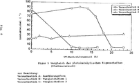
Vergleich 1 der photokatalytischen Eigenschaften
Die photokatalytischen Eigenschaften der obigen drei Arten von photokatalytischen Dünnfilmen wurden durch das Ölabbaufähigkeits-Bewertungsverfahren verglichen. Bei dem Ölabbaufähigkeits-Bewertungsverfahren wurde das Substrat, auf dem der photokatalytische Dünnfilm gebildet worden war, 24 Stunden lang mit UV-Strahlen (Spitzenwellenlänge 350 nm) bestrahlt, reines Wasser quantitativ aufgetropft und der Kontaktwinkel mit einer Kontaktwinkelvorrichtung gemessen, und dann Öl auf das Substrat, an dem das reine Wasser getrocknet war, getropft und an der Vorderfläche verstrichen, eine zehnstündige Bestrahlung mit UV-Strahlen (Spitzenwellenlänge 350 nm) vorgenommen, reines Wasser aufgetropft und erneut der Kontaktwinkel mit einer Kontaktwinkelmessvorrichtung gemessen.
Wie in
Vergleich 2 der photokatalytischen Eigenschaften
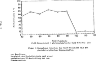
Für den photokatalytischen Dünnfilm der vorliegenden Erfindung wurde ein Basismaterial vorbereitet, bei dem die TiO2-Filmdicke stufenweise von 40 nm bis 120 nm verändert worden war. Dann wurde eine Bewertung nach dem obigen Ölabbaufähigkeits-Bewertungsverfahren vorgenommen. Die Ergebnisse sind in
Wie in
Da bei dem photokatalytischen mehrschichtigen Metallverbindungs-Dünnfilm der vorliegenden Erfindung und dem Verfahren zu seiner Herstellung wie oben beschrieben keine Plasmabehandlung des Substrats durch ein reaktives Gas und keine Erhitzungsbehandlung erfolgt, kann ein photokatalytischer Dünnfilm mit hohen photokatalytischen Eigenschaften bei einer niedrigen Temperatur gebildet werden. Daher wird auch eine Filmbildung bei einem Substrat aus Harz möglich. Überdies genügt es, wenn die gesamte Filmdicke der auf der Oberfläche des Substrats gebildeten Keimschicht aus einem amorphen Metallverbindungs-Dünnfilm und des auf der Keimschicht gebildeten kristallinen Metallverbindungs-Dünnfilms mindestens 100 nm beträgt, weshalb die Hydrophilizität und die Ölabbaufähigkeit verglichen mit einem herkömmlichen photokatalytischen Dünnfilm bei einer weniger als halb so dicken Filmdicke in einer kurzen Zeit erreicht werden kann und eine rasche und billige Filmbildung möglich ist.Since the photocatalytic multilayer metal compound thin film of the present invention and the method of producing the same as described above do not plasma-treat the substrate with a reactive gas and heat treatment, a photocatalytic thin film having high photocatalytic properties can be formed at a low temperature. Therefore, film formation on a resin substrate becomes possible. Moreover, it suffices if the total film thickness of the seed layer made of an amorphous metal compound thin film and the crystalline metal compound thin film formed on the surface of the substrate is at least 100 nm, therefore, the hydrophilicity and the oil degradability are compared with a conventional photocatalytic thin film a film thickness less than half as thick can be achieved in a short time and rapid and inexpensive film formation is possible.
BezugszeichenlisteLIST OF REFERENCE NUMBERS
- 11
- Sputtervorrichtungsputtering
- 22
- Vakuumbehältervacuum vessel
- 33
- Rotationstrommelrotary drum
- 4a, 4b4a, 4b
- Sputtermittelsputtering means
- 55
- Vorrichtung zur Erzeugung einer aktivierten SpeziesDevice for generating an activated species
- 6a, 6b, 6c6a, 6b, 6c
- Trennwandpartition wall
- 7a, 7b7a, 7b
- FilmbildungsprozessbereichFilm formation process area
- 88th
- ReaktionsprozessbereichReaction process area
- 9a, 9b9a, 9b
- Mittel zur Lieferung von SputtergasMeans for supplying sputtering gas
- 1010
- Mittel zur Lieferung eines reaktiven GasesMeans for supplying a reactive gas
- 11a, 11b11a, 11b
- ArgongasflascheArgon gas cylinder
- 1212
- SauerstoffgasflascheOxygen gas cylinder
- 1313
- ArgongasflascheArgon gas cylinder
- 1414
- GasdurchflussmengenreglerGas flow regulator
- 1515
- WechselstromquelleAC power source
- 1616
- HochfrequenzstromquelleHigh frequency power source
- 17a, 17b17a, 17b
- Targettarget
- 2020
- Glassubstratglass substrate
- 2121
- Titanoxid-DünnfilmTitanium oxide thin film
- 2222
- Titanoxid-DünnfilmTitanium oxide thin film
- 2323
- Siliziumoxid-DünnfilmSilicon thin film
Claims (6)
Applications Claiming Priority (3)
| Application Number | Priority Date | Filing Date | Title |
|---|---|---|---|
| JP2009193027A JP5217023B2 (en) | 2009-08-24 | 2009-08-24 | Photocatalytic multilayer metal compound thin film and method for producing the same |
| JP2009-193027 | 2009-08-24 | ||
| PCT/JP2010/064201 WO2011024764A1 (en) | 2009-08-24 | 2010-08-23 | Photocatalytic multilayer metal compound thin film and method for producing same |
Publications (1)
| Publication Number | Publication Date |
|---|---|
| DE112010003373T5 true DE112010003373T5 (en) | 2012-07-19 |
Family
ID=43627869
Family Applications (1)
| Application Number | Title | Priority Date | Filing Date |
|---|---|---|---|
| DE112010003373T Withdrawn DE112010003373T5 (en) | 2009-08-24 | 2010-08-23 | Photocatalytic multi-layer metal compound thin film and process for its production |
Country Status (6)
| Country | Link |
|---|---|
| US (1) | US20120172196A1 (en) |
| JP (1) | JP5217023B2 (en) |
| KR (1) | KR20120082877A (en) |
| CN (1) | CN102575337B (en) |
| DE (1) | DE112010003373T5 (en) |
| WO (1) | WO2011024764A1 (en) |
Families Citing this family (3)
| Publication number | Priority date | Publication date | Assignee | Title |
|---|---|---|---|---|
| US20190010602A1 (en) * | 2015-12-30 | 2019-01-10 | Corning Incorporated | Methods and apparatuses to clamp cover substrates in a vacuum coating process with van der waals forces |
| FR3051804B1 (en) * | 2016-05-24 | 2018-06-29 | Saint-Gobain Glass France | THIN LAYER DEPOSITION METHOD |
| GB2600168A (en) * | 2020-10-26 | 2022-04-27 | Pilkington Group Ltd | Use of coated substrates |
Family Cites Families (8)
| Publication number | Priority date | Publication date | Assignee | Title |
|---|---|---|---|---|
| JP4214327B2 (en) * | 1997-07-14 | 2009-01-28 | 株式会社ブリヂストン | Method for producing titanium oxide film and photocatalytic film |
| JP2000143300A (en) * | 1998-11-09 | 2000-05-23 | Nikon Corp | Antifogging thin film and its preparation |
| CN1620336A (en) * | 2001-12-21 | 2005-05-25 | 日本板硝子株式会社 | Member having photocatalytic function and method for manufacture thereof |
| JP2003311157A (en) * | 2002-04-18 | 2003-11-05 | Toyota Central Res & Dev Lab Inc | Metal oxide photocatalytic body and manufacturing method therefor |
| US20070031681A1 (en) * | 2003-06-20 | 2007-02-08 | Nippon Sheet Glass Co., Ltd. | Member having photocatalytic activity and multilayered glass |
| CN101072735B (en) * | 2004-12-06 | 2011-08-10 | 日本板硝子株式会社 | Glass member having photocatalytic function and heat ray reflective function, and double layer glass employing it |
| JP4789700B2 (en) * | 2006-05-25 | 2011-10-12 | 株式会社シンクロン | Method for producing hydrophilic thin film |
| KR100811432B1 (en) * | 2006-11-09 | 2008-03-12 | 썬텍 주식회사 | Hydrophilic mirror coated tio2 membrane on chrome plate |
-
2009
- 2009-08-24 JP JP2009193027A patent/JP5217023B2/en active Active
-
2010
- 2010-08-23 US US13/391,564 patent/US20120172196A1/en not_active Abandoned
- 2010-08-23 WO PCT/JP2010/064201 patent/WO2011024764A1/en active Application Filing
- 2010-08-23 KR KR1020127007636A patent/KR20120082877A/en not_active Application Discontinuation
- 2010-08-23 CN CN201080037641.4A patent/CN102575337B/en active Active
- 2010-08-23 DE DE112010003373T patent/DE112010003373T5/en not_active Withdrawn
Non-Patent Citations (1)
| Title |
|---|
| "Thickness depencence of TiO2 films deposited by Oxygen ion assisted reactive evaporation method", Shôhei MOCHIZUKI; Tetsuya KAGAMI; Taiki ISHIHARA; Noriyuki SATÔ; Kôji, KOBAYASHI; Takeshi MAEDA; Yôichi HOSHI: wissenschaftliche Vorträge bei der 69. Konferenz für Angewandte Physik, 3a-J-8 (September 2008) |
Also Published As
| Publication number | Publication date |
|---|---|
| US20120172196A1 (en) | 2012-07-05 |
| WO2011024764A1 (en) | 2011-03-03 |
| CN102575337A (en) | 2012-07-11 |
| JP5217023B2 (en) | 2013-06-19 |
| KR20120082877A (en) | 2012-07-24 |
| JP2011042854A (en) | 2011-03-03 |
| CN102575337B (en) | 2014-11-26 |
Similar Documents
| Publication | Publication Date | Title |
|---|---|---|
| DE60104026T2 (en) | Method for applying a coating by physical vapor deposition | |
| EP2102381B1 (en) | Method for the production of an antimicrobial material | |
| WO2013113518A1 (en) | Hydrophilizing plasma coating method | |
| WO2005073427A2 (en) | Method for the production of an ultra barrier layer system | |
| DE112010003373T5 (en) | Photocatalytic multi-layer metal compound thin film and process for its production | |
| DE102008016969B3 (en) | Method for producing a layer by cold gas spraying | |
| WO2009127373A1 (en) | Transparent barrier layer system | |
| DE69916956T2 (en) | METHOD FOR PRODUCING THIN FILMS FROM OXIDIC CERAMICS | |
| DE102009053756B4 (en) | Process for coating a substrate in a vacuum chamber with at least one rotating magnetron | |
| EP2435599A2 (en) | Method for fabricating a layer with absorbing particles for an energy radiation | |
| DE102006019000A1 (en) | Device and method for plasma-assisted deposition of hard material layers | |
| EP1458654B1 (en) | Method for the production of locally functional areas and objects obtained therewith | |
| EP3133184B1 (en) | Method of forming a layer having high light transmission and/or low light reflection | |
| DE102016104128A1 (en) | Method for coating a component surface, coated component and use of a precursor material | |
| EP1838640A2 (en) | Fine-laminar barrier protection layer | |
| DE102017121684A1 (en) | Method for creating a structured surface | |
| DE3925085C1 (en) | ||
| EP3402910A2 (en) | Process for producing a thin layer of porous dlc, use of a pecvd plant and workpiece coated with porous dlc | |
| WO2007118463A1 (en) | Method and device for depositing diamond-like carbon coatings with a predetermined hardness progression on substrates | |
| DE102004016436B3 (en) | Process of manufacturing self-cleaning window glass or glass building facade involves atomised application of silicon agent to titanium oxide surface | |
| WO2018158037A1 (en) | Method for producing patterned layers | |
| WO2018072774A1 (en) | Device and method for producing defined properties of gradient layers in a system of multilayered coatings in sputtering installations | |
| DE112016001220T5 (en) | Non-metallic coating for steel substrates and method for forming same | |
| DE102015210827B4 (en) | Process for the formation of structures on the surfaces of a component | |
| DE10239163A1 (en) | Device and method for forming gradient layers on substrates in a vacuum chamber |
Legal Events
| Date | Code | Title | Description |
|---|---|---|---|
| R163 | Identified publications notified | ||
| R082 | Change of representative |
Representative=s name: PATENTANWAELTE LIPPERT, STACHOW & PARTNER, DE |
|
| R081 | Change of applicant/patentee |
Owner name: KABUSHIKI KAISHA HONDA LOCK, JP Free format text: FORMER OWNER: INSTITUTE OF NATIONAL COLLEGES , KABUSHIKI KAISHA HONDA LOCK, , JP Effective date: 20120829 Owner name: CHINCRON CO., LTD., JP Free format text: FORMER OWNER: INSTITUTE OF NATIONAL COLLEGES , KABUSHIKI KAISHA HONDA LOCK, , JP Effective date: 20120829 Owner name: INSTITUTE OF NATIONAL COLLEGES OF TECHNOLOGY, , JP Free format text: FORMER OWNER: INSTITUTE OF NATIONAL COLLEGES , KABUSHIKI KAISHA HONDA LOCK, , JP Effective date: 20120829 Owner name: SHINCRON CO. LTD., JP Free format text: FORMER OWNER: INSTITUTE OF NATIONAL COLLEGES , KABUSHIKI KAISHA HONDA LOCK, , JP Effective date: 20120829 Owner name: SHINCRON CO. LTD., YOKOHAMA-SHI, JP Free format text: FORMER OWNER: INSTITUTE OF NATIONAL COLLEGES , KABUSHIKI KAISHA HONDA LOCK, , JP Effective date: 20120829 Owner name: KABUSHIKI KAISHA HONDA LOCK, MIYAZAKI-CITY, JP Free format text: FORMER OWNER: INSTITUTE OF NATIONAL COLLEGES , KABUSHIKI KAISHA HONDA LOCK, , JP Effective date: 20120829 Owner name: INSTITUTE OF NATIONAL COLLEGES OF TECHNOLOGY, , JP Free format text: FORMER OWNERS: INSTITUTE OF NATIONAL COLLEGES OF TECHNOLOGY, JAPAN, HACHIOJI-CITY, TOKYO, JP; KABUSHIKI KAISHA HONDA LOCK, MIYAZAKI-CITY, MIYAZAKI, JP Effective date: 20120829 Owner name: KABUSHIKI KAISHA HONDA LOCK, MIYAZAKI-CITY, JP Free format text: FORMER OWNERS: INSTITUTE OF NATIONAL COLLEGES OF TECHNOLOGY, JAPAN, HACHIOJI-CITY, TOKYO, JP; KABUSHIKI KAISHA HONDA LOCK, MIYAZAKI-CITY, MIYAZAKI, JP Effective date: 20120829 Owner name: SHINCRON CO. LTD., YOKOHAMA-SHI, JP Free format text: FORMER OWNERS: INSTITUTE OF NATIONAL COLLEGES OF TECHNOLOGY, JAPAN, HACHIOJI-CITY, TOKYO, JP; KABUSHIKI KAISHA HONDA LOCK, MIYAZAKI-CITY, MIYAZAKI, JP Effective date: 20120829 |
|
| R082 | Change of representative |
Representative=s name: PATENTANWAELTE LIPPERT, STACHOW & PARTNER, DE Effective date: 20120829 Representative=s name: LIPPERT STACHOW PATENTANWAELTE RECHTSANWAELTE , DE Effective date: 20120829 |
|
| R081 | Change of applicant/patentee |
Owner name: INSTITUTE OF NATIONAL COLLEGES OF TECHNOLOGY, , JP Free format text: FORMER OWNER: CHINCRON CO., LTD., INSTITUTE OF NATIONAL COLLEGES , KABUSHIKI KAISHA HONDA LOCK, , JP Effective date: 20131002 Owner name: KABUSHIKI KAISHA HONDA LOCK, JP Free format text: FORMER OWNER: CHINCRON CO., LTD., INSTITUTE OF NATIONAL COLLEGES , KABUSHIKI KAISHA HONDA LOCK, , JP Effective date: 20131002 Owner name: SHINCRON CO. LTD., JP Free format text: FORMER OWNER: CHINCRON CO., LTD., INSTITUTE OF NATIONAL COLLEGES , KABUSHIKI KAISHA HONDA LOCK, , JP Effective date: 20131002 Owner name: SHINCRON CO. LTD., YOKOHAMA-SHI, JP Free format text: FORMER OWNER: CHINCRON CO., LTD., INSTITUTE OF NATIONAL COLLEGES , KABUSHIKI KAISHA HONDA LOCK, , JP Effective date: 20131002 Owner name: KABUSHIKI KAISHA HONDA LOCK, MIYAZAKI-CITY, JP Free format text: FORMER OWNER: CHINCRON CO., LTD., INSTITUTE OF NATIONAL COLLEGES , KABUSHIKI KAISHA HONDA LOCK, , JP Effective date: 20131002 Owner name: KABUSHIKI KAISHA HONDA LOCK, MIYAZAKI-CITY, JP Free format text: FORMER OWNERS: CHINCRON CO., LTD., YOKOHAMA-CITY, KANAGAWA, JP; INSTITUTE OF NATIONAL COLLEGES OF TECHNOLOGY, JAPAN, HACHIOJI-CITY, TOKYO, JP; KABUSHIKI KAISHA HONDA LOCK, MIYAZAKI-CITY, MIYAZAKI, JP Effective date: 20131002 Owner name: SHINCRON CO. LTD., YOKOHAMA-SHI, JP Free format text: FORMER OWNERS: CHINCRON CO., LTD., YOKOHAMA-CITY, KANAGAWA, JP; INSTITUTE OF NATIONAL COLLEGES OF TECHNOLOGY, JAPAN, HACHIOJI-CITY, TOKYO, JP; KABUSHIKI KAISHA HONDA LOCK, MIYAZAKI-CITY, MIYAZAKI, JP Effective date: 20131002 Owner name: INSTITUTE OF NATIONAL COLLEGES OF TECHNOLOGY, , JP Free format text: FORMER OWNERS: CHINCRON CO., LTD., YOKOHAMA-CITY, KANAGAWA, JP; INSTITUTE OF NATIONAL COLLEGES OF TECHNOLOGY, JAPAN, HACHIOJI-CITY, TOKYO, JP; KABUSHIKI KAISHA HONDA LOCK, MIYAZAKI-CITY, MIYAZAKI, JP Effective date: 20131002 |
|
| R082 | Change of representative |
Representative=s name: PATENTANWAELTE LIPPERT, STACHOW & PARTNER, DE Effective date: 20131002 Representative=s name: LIPPERT STACHOW PATENTANWAELTE RECHTSANWAELTE , DE Effective date: 20131002 |
|
| R119 | Application deemed withdrawn, or ip right lapsed, due to non-payment of renewal fee |