DE10328811A1 - A compound for forming a self-assembling monolayer, a layered structure, a semiconductor device having a layered structure and a method for producing a layered structure - Google Patents
A compound for forming a self-assembling monolayer, a layered structure, a semiconductor device having a layered structure and a method for producing a layered structure Download PDFInfo
- Publication number
- DE10328811A1 DE10328811A1 DE10328811A DE10328811A DE10328811A1 DE 10328811 A1 DE10328811 A1 DE 10328811A1 DE 10328811 A DE10328811 A DE 10328811A DE 10328811 A DE10328811 A DE 10328811A DE 10328811 A1 DE10328811 A1 DE 10328811A1
- Authority
- DE
- Germany
- Prior art keywords
- monolayer
- group
- layer
- substrate
- dielectric
- Prior art date
- Legal status (The legal status is an assumption and is not a legal conclusion. Google has not performed a legal analysis and makes no representation as to the accuracy of the status listed.)
- Granted
Links
Classifications
-
- G—PHYSICS
- G03—PHOTOGRAPHY; CINEMATOGRAPHY; ANALOGOUS TECHNIQUES USING WAVES OTHER THAN OPTICAL WAVES; ELECTROGRAPHY; HOLOGRAPHY
- G03F—PHOTOMECHANICAL PRODUCTION OF TEXTURED OR PATTERNED SURFACES, e.g. FOR PRINTING, FOR PROCESSING OF SEMICONDUCTOR DEVICES; MATERIALS THEREFOR; ORIGINALS THEREFOR; APPARATUS SPECIALLY ADAPTED THEREFOR
- G03F7/00—Photomechanical, e.g. photolithographic, production of textured or patterned surfaces, e.g. printing surfaces; Materials therefor, e.g. comprising photoresists; Apparatus specially adapted therefor
- G03F7/16—Coating processes; Apparatus therefor
- G03F7/165—Monolayers, e.g. Langmuir-Blodgett
-
- H—ELECTRICITY
- H10—SEMICONDUCTOR DEVICES; ELECTRIC SOLID-STATE DEVICES NOT OTHERWISE PROVIDED FOR
- H10P—GENERIC PROCESSES OR APPARATUS FOR THE MANUFACTURE OR TREATMENT OF DEVICES COVERED BY CLASS H10
- H10P50/00—Etching of wafers, substrates or parts of devices
-
- B—PERFORMING OPERATIONS; TRANSPORTING
- B82—NANOTECHNOLOGY
- B82Y—SPECIFIC USES OR APPLICATIONS OF NANOSTRUCTURES; MEASUREMENT OR ANALYSIS OF NANOSTRUCTURES; MANUFACTURE OR TREATMENT OF NANOSTRUCTURES
- B82Y10/00—Nanotechnology for information processing, storage or transmission, e.g. quantum computing or single electron logic
-
- C—CHEMISTRY; METALLURGY
- C03—GLASS; MINERAL OR SLAG WOOL
- C03C—CHEMICAL COMPOSITION OF GLASSES, GLAZES OR VITREOUS ENAMELS; SURFACE TREATMENT OF GLASS; SURFACE TREATMENT OF FIBRES OR FILAMENTS MADE FROM GLASS, MINERALS OR SLAGS; JOINING GLASS TO GLASS OR OTHER MATERIALS
- C03C17/00—Surface treatment of glass, not in the form of fibres or filaments, by coating
- C03C17/28—Surface treatment of glass, not in the form of fibres or filaments, by coating with organic material
- C03C17/30—Surface treatment of glass, not in the form of fibres or filaments, by coating with organic material with silicon-containing compounds
-
- C—CHEMISTRY; METALLURGY
- C03—GLASS; MINERAL OR SLAG WOOL
- C03C—CHEMICAL COMPOSITION OF GLASSES, GLAZES OR VITREOUS ENAMELS; SURFACE TREATMENT OF GLASS; SURFACE TREATMENT OF FIBRES OR FILAMENTS MADE FROM GLASS, MINERALS OR SLAGS; JOINING GLASS TO GLASS OR OTHER MATERIALS
- C03C17/00—Surface treatment of glass, not in the form of fibres or filaments, by coating
- C03C17/34—Surface treatment of glass, not in the form of fibres or filaments, by coating with at least two coatings having different compositions
- C03C17/36—Surface treatment of glass, not in the form of fibres or filaments, by coating with at least two coatings having different compositions at least one coating being a metal
- C03C17/38—Surface treatment of glass, not in the form of fibres or filaments, by coating with at least two coatings having different compositions at least one coating being a metal at least one coating being a coating of an organic material
-
- C—CHEMISTRY; METALLURGY
- C07—ORGANIC CHEMISTRY
- C07F—ACYCLIC, CARBOCYCLIC OR HETEROCYCLIC COMPOUNDS CONTAINING ELEMENTS OTHER THAN CARBON, HYDROGEN, HALOGEN, OXYGEN, NITROGEN, SULFUR, SELENIUM OR TELLURIUM
- C07F7/00—Compounds containing elements of Groups 4 or 14 of the Periodic Table
- C07F7/02—Silicon compounds
- C07F7/08—Compounds having one or more C—Si linkages
- C07F7/12—Organo silicon halides
-
- C—CHEMISTRY; METALLURGY
- C07—ORGANIC CHEMISTRY
- C07F—ACYCLIC, CARBOCYCLIC OR HETEROCYCLIC COMPOUNDS CONTAINING ELEMENTS OTHER THAN CARBON, HYDROGEN, HALOGEN, OXYGEN, NITROGEN, SULFUR, SELENIUM OR TELLURIUM
- C07F7/00—Compounds containing elements of Groups 4 or 14 of the Periodic Table
- C07F7/02—Silicon compounds
- C07F7/08—Compounds having one or more C—Si linkages
- C07F7/18—Compounds having one or more C—Si linkages as well as one or more C—O—Si linkages
- C07F7/1804—Compounds having Si-O-C linkages
-
- H—ELECTRICITY
- H10—SEMICONDUCTOR DEVICES; ELECTRIC SOLID-STATE DEVICES NOT OTHERWISE PROVIDED FOR
- H10K—ORGANIC ELECTRIC SOLID-STATE DEVICES
- H10K10/00—Organic devices specially adapted for rectifying, amplifying, oscillating or switching; Organic capacitors or resistors having potential barriers
- H10K10/40—Organic transistors
- H10K10/46—Field-effect transistors, e.g. organic thin-film transistors [OTFT]
- H10K10/462—Insulated gate field-effect transistors [IGFETs]
- H10K10/466—Lateral bottom-gate IGFETs comprising only a single gate
-
- H—ELECTRICITY
- H10—SEMICONDUCTOR DEVICES; ELECTRIC SOLID-STATE DEVICES NOT OTHERWISE PROVIDED FOR
- H10K—ORGANIC ELECTRIC SOLID-STATE DEVICES
- H10K10/00—Organic devices specially adapted for rectifying, amplifying, oscillating or switching; Organic capacitors or resistors having potential barriers
- H10K10/40—Organic transistors
- H10K10/46—Field-effect transistors, e.g. organic thin-film transistors [OTFT]
- H10K10/462—Insulated gate field-effect transistors [IGFETs]
- H10K10/468—Insulated gate field-effect transistors [IGFETs] characterised by the gate dielectrics
-
- H—ELECTRICITY
- H10—SEMICONDUCTOR DEVICES; ELECTRIC SOLID-STATE DEVICES NOT OTHERWISE PROVIDED FOR
- H10K—ORGANIC ELECTRIC SOLID-STATE DEVICES
- H10K10/00—Organic devices specially adapted for rectifying, amplifying, oscillating or switching; Organic capacitors or resistors having potential barriers
- H10K10/701—Organic molecular electronic devices
-
- H—ELECTRICITY
- H10—SEMICONDUCTOR DEVICES; ELECTRIC SOLID-STATE DEVICES NOT OTHERWISE PROVIDED FOR
- H10K—ORGANIC ELECTRIC SOLID-STATE DEVICES
- H10K85/00—Organic materials used in the body or electrodes of devices covered by this subclass
- H10K85/701—Langmuir Blodgett films
-
- H—ELECTRICITY
- H10—SEMICONDUCTOR DEVICES; ELECTRIC SOLID-STATE DEVICES NOT OTHERWISE PROVIDED FOR
- H10P—GENERIC PROCESSES OR APPARATUS FOR THE MANUFACTURE OR TREATMENT OF DEVICES COVERED BY CLASS H10
- H10P10/00—Bonding of wafers, substrates or parts of devices
-
- B—PERFORMING OPERATIONS; TRANSPORTING
- B05—SPRAYING OR ATOMISING IN GENERAL; APPLYING FLUENT MATERIALS TO SURFACES, IN GENERAL
- B05D—PROCESSES FOR APPLYING FLUENT MATERIALS TO SURFACES, IN GENERAL
- B05D1/00—Processes for applying liquids or other fluent materials
- B05D1/18—Processes for applying liquids or other fluent materials performed by dipping
- B05D1/185—Processes for applying liquids or other fluent materials performed by dipping applying monomolecular layers
-
- Y—GENERAL TAGGING OF NEW TECHNOLOGICAL DEVELOPMENTS; GENERAL TAGGING OF CROSS-SECTIONAL TECHNOLOGIES SPANNING OVER SEVERAL SECTIONS OF THE IPC; TECHNICAL SUBJECTS COVERED BY FORMER USPC CROSS-REFERENCE ART COLLECTIONS [XRACs] AND DIGESTS
- Y10—TECHNICAL SUBJECTS COVERED BY FORMER USPC
- Y10S—TECHNICAL SUBJECTS COVERED BY FORMER USPC CROSS-REFERENCE ART COLLECTIONS [XRACs] AND DIGESTS
- Y10S977/00—Nanotechnology
- Y10S977/902—Specified use of nanostructure
- Y10S977/932—Specified use of nanostructure for electronic or optoelectronic application
- Y10S977/936—Specified use of nanostructure for electronic or optoelectronic application in a transistor or 3-terminal device
Landscapes
- Chemical & Material Sciences (AREA)
- Organic Chemistry (AREA)
- Engineering & Computer Science (AREA)
- Physics & Mathematics (AREA)
- Materials Engineering (AREA)
- Chemical Kinetics & Catalysis (AREA)
- Nanotechnology (AREA)
- General Chemical & Material Sciences (AREA)
- Life Sciences & Earth Sciences (AREA)
- Geochemistry & Mineralogy (AREA)
- General Physics & Mathematics (AREA)
- Crystallography & Structural Chemistry (AREA)
- Mathematical Physics (AREA)
- Theoretical Computer Science (AREA)
- Spectroscopy & Molecular Physics (AREA)
- Thin Film Transistor (AREA)
- Bipolar Transistors (AREA)
- Liquid Deposition Of Substances Of Which Semiconductor Devices Are Composed (AREA)
Abstract
Die Erfindung betrifft eine Verbindung zur Bildung einer selbstorganisierenden Monolage, insbesondere einer Monolage für ein Halbleiterbauelement, gekennzeichnet durch eine molekulare Gruppe mit der Fähigkeit einer PI-PI Wechselwirkung (3) mit anderen Verbindungen der gleichen Art und/oder Verbindungen anderer Art zur Stabilisierung der Monolage (11). Ferner betrifft die Erfindung auch eine Schichtstruktur, ein Halbleiterbauelement und ein Verfahren zur Herstellung einer Schichtstruktur. Damit ist eine effiziente Herstellung eines Halbleiterbauelementes, insbesondere eines organischen Feldeffekttransistors, möglich.The invention relates to a compound for forming a self-assembling monolayer, in particular a monolayer for a semiconductor device, characterized by a molecular group having the ability of a PI-PI interaction (3) with other compounds of the same kind and / or compounds of another kind for stabilizing the monolayer (11). Furthermore, the invention also relates to a layer structure, a semiconductor component and a method for producing a layer structure. For an efficient production of a semiconductor device, in particular an organic field effect transistor is possible.
Description
Die Erfindung betrifft eine Verbindung zur Bildung einer selbstorganisierenden Monolage nach dem Oberbegriff des Anspruchs 1, eine Schichtstruktur nach Anspruch 11, ein Halbleiterbauelement nach Anspruch 17 und ein Verfahren zur Herstellung einer Schichtstruktur nach Anspruch 19.The The invention relates to a compound for forming a self-organizing Monolayer according to the preamble of claim 1, a layer structure according to claim 11, a semiconductor device according to claim 17 and a method for producing a layered structure according to claim 19th
Feldeffekttransistoren auf der Basis organischer Halbleiter (OFET) sind für eine Vielzahl elektronischer Anwendungen von Interesse. Insbesondere sind damit niedrige Fertigungskosten, flexible oder unzerbrechliche Substrate, oder die Herstellung von Transistoren und integrierten Schaltungen über große aktive Flächen möglich. Zum Beispiel eignen sich organische Feldeffekt-Transistoren als Pixel-Steuerelemente in Aktiv-Matrix-Bildschirmen oder für die Herstellung von extrem preiswerten integrierten Schaltungen, wie sie zum Beispiel für die aktive Kennzeichnung und Identifizierung von Waren und Gütern zum Einsatz kommen.FETs On the basis of organic semiconductors (OFET) are available for a variety electronic applications of interest. In particular, they are low production costs, flexible or unbreakable substrates, or the production of transistors and integrated circuits over large active Surfaces possible. To the For example, organic field effect transistors are suitable as pixel controls in active matrix screens or for the production of extremely low-cost integrated circuits, as for example the active identification and identification of goods and goods for Use come.
Da sich mit organischen Feldeffekttransistoren komplexe Schaltungen aufbauen lassen, bestehen zahlreiche Anwendungsmöglichkeiten. So gilt beispielsweise die Einführung von RF-ID (RF-ID: radio frequency identification) Systemen basierend auf dieser Technologie als potentieller Ersatz für den störanfälligen und nur in direktem Sichtkontakt zum Scanner anwendbaren Barcode. Passive RF-ID Systeme beziehen ihre Energie aus dem eingestrahlten Wechselfeld. Der mögliche Abstand zwischen Lesegerät und Transponder hängt dabei von der abgestrahlten Leistung und dem Energiebedarf des Transponders ab. Siliziumbasierte Transponder arbeiten deshalb bei Versorgungsspannungen um 3V. Produkte, die einen siliziumbasierten Chip enthalten, sind für viele Anwendungen zu teuer. Beispielsweise kommt für die Kennzeichnung von Lebensmitteln (Preis, Verfallsdatum etc.) ein siliziumbasiertes Ident-Tag nicht in Betracht.There complex circuits with organic field effect transistors can be built up, there are numerous applications. For example the introduction based on RF-ID (RF-ID: radio frequency identification) systems on this technology as a potential replacement for the susceptible and only in direct Visual contact with the scanner applicable barcode. Passive RF-ID systems draw their energy from the radiated alternating field. The possible distance between reader and transponder is attached the radiated power and the energy consumption of the transponder from. Silicon-based transponders therefore operate at supply voltages around 3V. Products containing a silicon-based chip are for many Applications too expensive. For example, for the labeling of food (price, Expiration date, etc.), a silicon-based identification tag is not possible.
Organische Feldeffekttransistoren bestehen normalerweise aus mindestens vier verschiedenen, übereinander aufgebrachten Schichten: einer Gateelektrode, einem Dielektrikum, einer Source-Drain-Kontaktschicht und einem organischen Halbleiter. Die Reihenfolge der Schichten kann dabei variieren. Damit die Funktionalität entsteht, müssen die einzelnen Lagen strukturiert werden, was relativ aufwändig ist.organic Field effect transistors usually consist of at least four different, one above the other applied layers: a gate electrode, a dielectric, a source-drain contact layer and an organic semiconductor. The order of the layers can vary. For the functionality to emerge, have to the individual layers are structured, which is relatively expensive.
Polymere bzw. organische Halbleiter bieten das Potential, dass billige Drucktechniken zu ihrer Strukturierung und Applikation eingesetzt werden können. Das Gatepotential zur Steuerung der organischen Feldeffekttransistoren kann umso kleiner gewählt werden, je dünner das Gatedielektrikum (d.h. eine dielektrische Schicht) hergestellt werden kann.polymers or organic semiconductors offer the potential that cheap printing techniques can be used for their structuring and application. The Gate potential for controlling the organic field effect transistors can be chosen smaller become, the thinner the gate dielectric (i.e., a dielectric layer) is fabricated can be.
In der Polymerelektronik wird die Dicke des Gatedielektrikums im Allgemeinen dahingehend optimiert, dass die Lösung eines Polymers immer dünner ausgeschleudert bzw. aufgedruckt wird (top-down). Diese Verfahrensweise stößt jedoch an ihre Grenzen, wenn Schichtdicken kleiner als 50 nm erzielt werden sollen.In The polymer electronics will be the thickness of the gate dielectric in general optimized so that the solution of a polymer thrown out ever thinner or printed (top-down). However, this procedure is encountered to their limits when layer thicknesses smaller than 50 nm are achieved should.
Es ist bekannt, Schichten für organische Feldeffekttransistoren mittels selbstorganisierenden Schichten aus molekularen Monolagen aufzubauen (SAM: Self-Assembled Monolayers).It is known, layers for organic field-effect transistors by means of self-organizing Build up layers of molecular monolayers (SAM: Self-Assembled Monolayers).
In den Artikeln von J. Collet, D. Vuillaume; "Nano-field effect transistor with an organic self-assembled monolayer as gate insulator", Applied Physics Letters 73 (1998) 2681; J. Collet, S. Lenfant, D. Vuillaume, O. Bouloussa, F. Rondelez, J. M. Gay, K. Kham, C. Chevrot; "High anisotropic conductivity in organic insulator/semiconductor monolayer heterostructure", Applied Physic Letters 76 (2000) 1339 und J. Collet, O. Tharaud, A. Chapoton, D. Vuillaume; "Lowvoltage, 30 nm channel length, organic transistors with a self-assembled monolayer as gate insulating films", Applied Physics Letters 76 (2000) 1941 werden solche Schichten beschrieben.In the articles by J. Collet, D. Vuillaume; "Nano-field effect transistor with an organic self-assembled monolayer as gate insulator ", Applied Physics Letters 73 (1998) 2681; J. Collet, S. Lenfant, D. Vuillaume, O. Bouloussa, F. Rondelez, J.M. Gay, K. Kham, C. Chevrot; "High anisotropic conductivity in organic insulator / semiconductor monolayer heterostructure ", Applied Physic Letters 76 (2000) 1339 and J. Collet, O. Tharaud, A. Chapoton, D. Vuillaume; "LowVoltage, 30 nm channel length, organic transistors with a self-assembled monolayer as gate insulation film ", Applied Physics Letters 76 (2000) In 1941 such layers are described.
Auch
in den Artikeln von Pradyt Ghosh, Richard M. Crooks; "Covalent Grafting
of a Pattered, Hyperbranched Polymer onto Plastic Substrate Using
Microcontact Printing",
J. Am. Chem. Soc. 121 (1999) 8395–8306; William M. Lackowski,
Pradyut Ghosh, Richard M. Crooks; "Micron-Scale Patterning of Hyperbranched
Polymer Films by Micro-Contact Printing;", J. Am. Chem. Soc. 121 (1999) 1419–1420 und
Jacob Sagiv; "Process
tor the production of built-up films by the stepwise adsorption
of individual monolayers",
In den Artikeln von Collet et al. werden Materialien beschrieben, mit denen sich Transistoren mit SAM-Schichten aufbauen lassen. Dabei bilden Vinyl-terminierte Silane als Ankergruppen auf hydroxylhaltigen Substratflächen eine SAM aus. Anschließend wird diese SAM chemisch nachbehandelt, um weitere Moleküle chemisch an die SAM zu binden (siehe Artikel von Sagiv et al.) oder es werden Oberflächen hergestellt, die eine weitere Prozessierung zulassen (siehe Artikel von Collet, Tharaud et al.).In the articles by Collet et al. describes materials that can be used to build transistors with SAM layers. Here, vinyl-terminated silanes form an SAM as anchor groups on hydroxyl-containing substrate surfaces. Subsequently, this SAM is chemically aftertreated to chemically bond additional molecules to the SAM (see article by Sagiv et al.) Or surfaces are prepared which allow further processing (see article by Collet, Tharaud et al.).
Dabei ist es nachteilig, dass diese Schichten nicht ohne Nachbehandlung eine dichte Dielektrikumsschicht bilden. Die eingesetzten chemischen Nachbehandlungen setzt bei einer Reaktionszeit von 48 bis 120 Stunden nur 70 bis 90% der Endgruppen um. Diese chemische Nachbehandlung dauert für die Fertigung hoher Stückzahlen zu lange.there it is disadvantageous that these layers are not without aftertreatment form a dense dielectric layer. The chemical used Post-treatment sets at a reaction time of 48 to 120 hours only 70 to 90% of the end groups around. This chemical aftertreatment lasts for the production of high quantities too long.
Prinzipiell
ist es auch möglich,
Polymere über
mehrere Koordinationsstellen an eine Oberfläche zu binden (Self-Assembled Polymers).
Dies ist aus der
Der vorliegenden Erfindung liegt die Aufgabe zugrunde, Mittel und Verfahren zur effizienten Herstellung eines Halbleiterbauelementes, insbesondere eines organischen Feldeffekttransistors zu schaffen.Of the The present invention is based on the object, means and methods for the efficient production of a semiconductor component, in particular to create an organic field effect transistor.
Diese Aufgabe wird erfindungsgemäß durch eine Verbindung mit den Merkmalen des Anspruchs 1 gelöst.These Task is achieved by a connection with the features of claim 1 solved.
Durch eine molekulare Gruppe mit der Fähigkeit einer π-π Wechselwirkung mit anderen Verbindungen der gleichen Art und/oder Verbindungen anderer Art kann eine Stabilisierung einer molekularen Monolage erreicht werden. Die π-π Wechselwirkung erlaubt die wechselseitige Bindung der einzelnen Moleküle in der Monolage untereinander.By a molecular group with the ability a π-π interaction with other compounds of the same type and / or compounds Another type can be a stabilization of a molecular monolayer be achieved. The π-π interaction allows the mutual binding of the individual molecules in the Monolayer among each other.
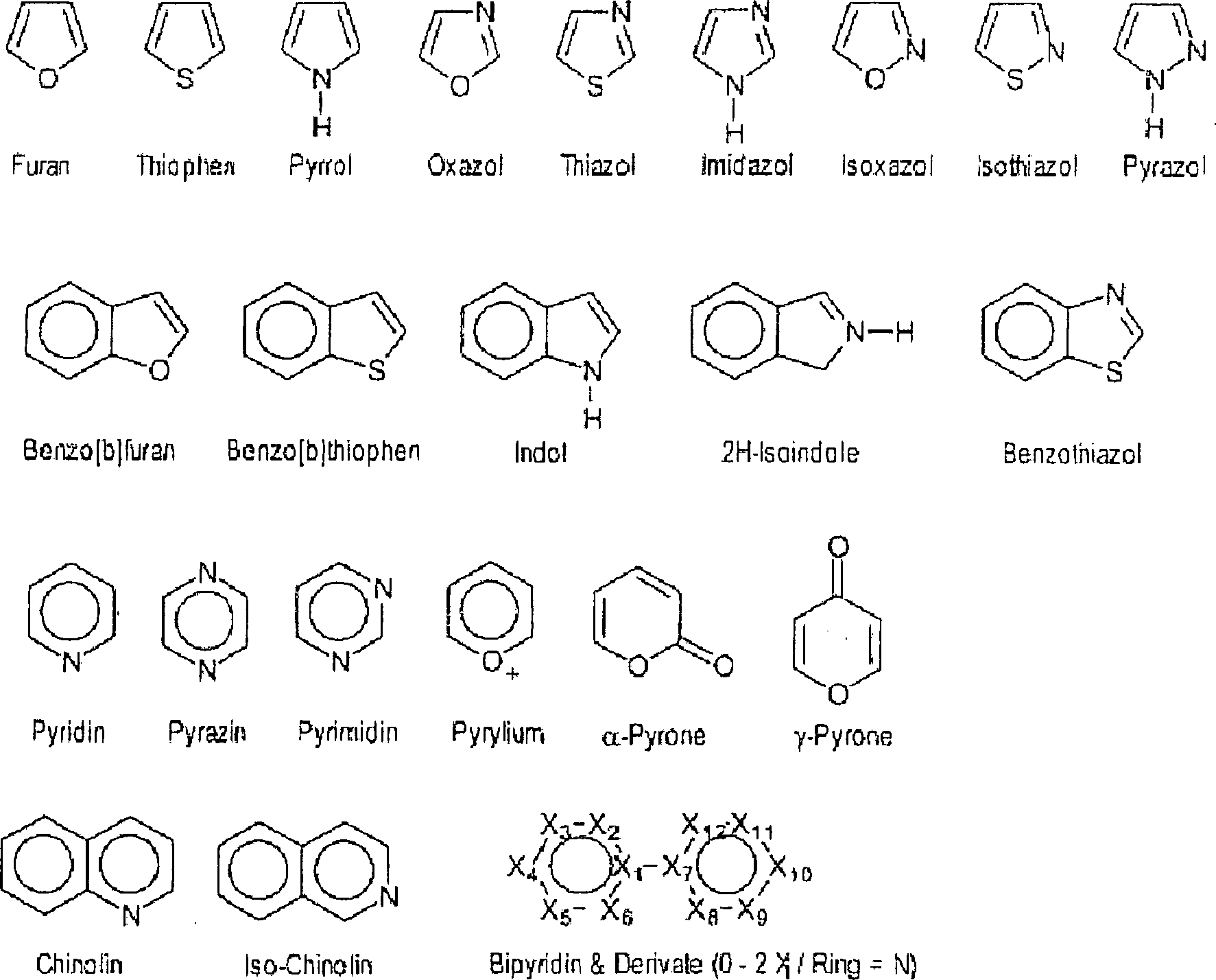
Dabei
ist es vorteilhaft, wenn die molekulare Gruppe mit der Fähigkeit
einer π-π Wechselwirkung
ein Aromat oder ein kondensiertes Aromat mit bis zu fünf Ringsystemen
aufweist, insbesondere ein Naphtalen, Anthracen, Naphtacen, Pentacen,
Biphenyl, Terphenyl, Quaterphenyl und/oder Quinquephenyl. Auch ist
es vorteilahft, wenn die molekulare Gruppe mit der Fähigkeit
einer π-π Wechselwirkung
mindestens eine der folgenden Gruppen aufweist: 
Mit Vorteil weist die Verbindung mindestens eine Ankergruppe zur Bindung an ein Substrat auf. Besonders vorteilhaft ist es, wenn eine Ankergruppe mindestens ein Silan, insbesondere ein Trichlorosilan, Dichlorosilan, ein Monochlorosilan, ein Trialkoxysilan, ein Dialkoxysilan und/oder ein Monoalkoxysilan aufweist.Advantageously, the compound has at least one anchor group for binding to a substrate. Be It is particularly advantageous if an anchor group has at least one silane, in particular a trichlorosilane, dichlorosilane, a monochlorosilane, a trialkoxysilane, a dialkoxysilane and / or a monoalkoxysilane.
Eine bevorzugte Ausführungsform des erfindungsgemäßen Moleküls ist im Wesentlichen linear aufgebaut ist und die molekulare Gruppe mit der Fähigkeit einer π-π Wechselwirkung ist als Kopfgruppe am von der Ankergruppe entfernten Ende der Verbindung angeordnet. Damit lassen sich Monolagen mit besonders stabiler Oberfläche erzeugen, so dass diese durch Verfahrensschritte strukturierbar ist.A preferred embodiment of the molecule according to the invention is in Is essentially linear and the molecular group with the ability a π-π interaction is the headgroup at the end of the connection away from the anchor group arranged. This allows monolayers to be produced with a particularly stable surface, so that it can be structured by method steps.
Vorteilhafterweise ist die Verbindung als ein ω-substituiertes Alkylchlorsilan, Alkoxysilane, ein ω-substituiertes Alkanthiol und/oder -selenol, insbesondere Phenoxyoctadecanthiol, sowie ein analoges Disulfid und Selenid ausgebildet. Es ist auch vorteilhaft, wenn die Verbindung als ω-Phenoxy-octadeclytrichlorsilan, ω-Biphenyloxyoctadeclytrichlorsilan und/oder ein Thienyloctadeclytrichlorsilan ausgebildet ist.advantageously, the compound is an ω-substituted Alkylchlorosilane, alkoxysilanes, an ω-substituted alkanethiol and / or selenol, in particular phenoxyoctadecanethiol, and a formed analog disulfide and selenide. It is also beneficial when the compound is ω-phenoxy-octadecyltrichlorosilane, ω-biphenyloxyoctadecyltrichlorosilane and / or a Thienyloctadeclytrichlorosilane is formed.
Wenn die erfindungsgemäße Verbindung eine dielektrische Gruppe, insbesondere zur Bildung einer dielektrischen Schicht in einer Monolage aufweist, so kann diese bei der Herstellung von Halbleiterbauelementen (z.B. einem OFET) verwendet werden. Dabei ist es vorteilhaft, wenn dielektrische Gruppe mindestens eine n-Alkylgruppe mit n = 2 bis 20 aufweist. Alkylgruppen weisen gute dielektrische Eigenschaften auf.If the compound of the invention a dielectric group, in particular for forming a dielectric Layer in a monolayer, it may in the production of semiconductor devices (e.g., an OFET). there it is advantageous if dielectric group at least one n-alkyl group with n = 2 to 20. Alkyl groups have good dielectric Properties on.
Die Aufgabe wird auch durch eine Schichtstruktur mit einer Monolage mit Verbindungen gemäß einem der Ansprüche 1 bis 10 gelöst. Diese Schichtstruktur kann Teil eines Halbleiterbauelemente sein oder ein komplettes Bauelement darstellen.The Task is also through a layered structure with a monolayer with compounds according to any one of claims 1 to 10 solved. This layer structure may be part of a semiconductor device or represent a complete component.
Dabei ist es vorteilhaft, wenn die Monolage auf ein Substrat mit einer metallischen Oberfläche, einer metalloxidischen Oberfläche und/oder einer Kunststoffoberfläche angeordnet ist. Besonders vorteilhaft ist es, wenn ein Substrat eine hydroxylgruppenhaltigen Oberfläche, insbesondere ein Substrat aus Silizium, Titan oder Aluminium, aufweist. An diese Oberflächen binden sich Ankergruppen in effizienter Weise.there It is advantageous if the monolayer on a substrate with a metallic surface, a metal oxide surface and / or a plastic surface is arranged. It is particularly advantageous if a substrate a hydroxyl-containing surface, in particular a substrate made of silicon, titanium or aluminum. Bind to these surfaces anchor groups in an efficient way.
Eine vorteilhafte Ausführungsform der erfindungsgemäßen Schichtstruktur weist folgende Schichten auf:
- a) die Monolage mit Ankergruppen, die mit dem Substrat verbunden ist,
- b) vom Substrat aus gesehen oberhalb der Ankergruppen eine Schicht aus dielektrischen Gruppen
- c) oberhalb der dielektrischen Gruppen eine Schicht aus molekularen Gruppen mit der Fähigkeit einer π-π Wechselwirkung.
- a) the monolayer with anchor groups connected to the substrate,
- b) seen from the substrate above the anchor groups, a layer of dielectric groups
- c) above the dielectric groups a layer of molecular groups with the ability of π-π interaction.
Zur Ausbildung einer gleichmäßigen Schichtenstruktur ist es vorteilhaft, wenn die Ankergruppe, die dielektrische Gruppe und die molekulare Gruppe mit einer Fähigkeit der π-π Wechselwirkung im wesentlichen die gleichen Längen aufweisen.to Formation of a uniform layer structure it is advantageous if the anchor group, the dielectric group and the molecular group with a capacity of π-π interaction essentially the same lengths exhibit.
Ferner ist es vorteilhaft, wenn auf eine Monolage mindestens eine weitere Schicht, insbesondere eine Metallschicht angeordnet ist.Further it is advantageous if on a monolayer at least one more Layer, in particular a metal layer is arranged.
Die Aufgabe wird auch durch ein Halbleiterbauelement mit einer Schichtstruktur nach mindestens einem der Ansprüche 11 bis 16 gelöst. Dabei ist es besonders vorteilhaft, wenn das Halbleiterbauelement als organischer Feldeffekttransistor aufgebaut ist und eine Monolage mit mindestens einer dielektrischen Schicht aufweist.The The object is also achieved by a semiconductor component with a layer structure according to at least one of the claims 11 to 16 solved. It is particularly advantageous if the semiconductor device is constructed as an organic field effect transistor and a monolayer having at least one dielectric layer.
Die Aufgabe wird auch durch ein Verfahren zur Herstellung einer Schichtstruktur nach mindestens einem der Ansprüche 11 bis 17 gelöst, in dem eine Monolage aus Verbindungen nach mindestens einem der Ansprüche 1 bis 10 aus einer flüssiger Phase oder einer Gasphase auf ein Substrat abgeschieden wird. Bei einem Abscheiden aus der Gasphase (verminderter Druck, erhöhte Temperatur) ergeben sich besonders hohe Dichten in den Schichten, was vorteilhaft ist.The The object is also achieved by a method for producing a layered structure according to at least one of the claims 11 to 17 solved, in which a monolayer of compounds according to at least one of claims 1 to 10 from a liquid Phase or a gas phase is deposited on a substrate. At a Separation from the gas phase (reduced pressure, elevated temperature) This results in particularly high densities in the layers, which is advantageous is.
Besonders vorteilhaft ist es, wenn eine Monolage aus Verbindungen nach mindestens einem der Ansprüche 1 bis 10 aus einer flüssigen Phase mit einem organischen Lösungsmittel in einem Tauchprozess abgeschieden wird.Especially It is advantageous if a monolayer of compounds according to at least one of the claims 1 to 10 from a liquid Phase with an organic solvent is deposited in a dipping process.
Die Erfindung wird nachfolgend unter Bezugnahme auf die Figuren der Zeichnungen an mehreren Ausführungsbeispielen näher erläutert. Es zeigen:The Invention will be described below with reference to the figures of Drawings on several embodiments explained in more detail. It demonstrate:
Tab. 1 Technologieparametervergleich zwischen organischen Feldeffekttransistoren mit erfindungsgemäßer Schichtstruktur und den Daten des 170 nm Knotens der Si-Technologie;Tab. 1 Technology parameter comparison between organic field effect transistors with layer structure according to the invention and the data of the 170 nm node of the Si technology;
Tab.
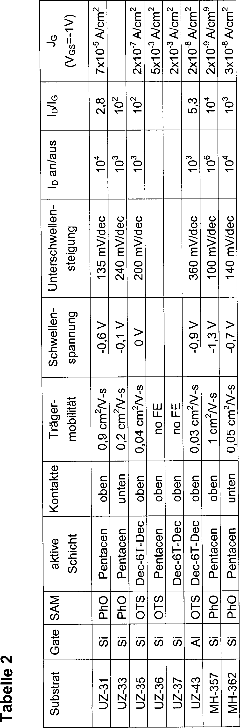
2 tabellarische Zusammenstellung der Versuchsergebnisse (
In
Dies
ist in
In
Auch
sind Ketten mit jeweils unterschiedlichen aromatischen Ringsystemen
in der Kette möglich. Über die
Länge der
kondensierten Ketten lassen sich die Eigenschaften gut einstellen.
Dabei sind kleinere, meist nicht hochkondensierte Aromaten, die
die im Wesentlichen einkristalline bzw. epitaktische zweidimensionale Struktur
der Monolage
Mittels
dieser Wechselwirkungen können
Schichten ausgebildet werden, die für Dielektrika in organischen
Feldeffekttransistoren gut geeignet sind. Im direkten Vergleich
(siehe
Die π-π Wechselwirkung
tritt bei den Monolagen
Die
Leckströme
derartiger T-SAMs sind so gering, dass sie als Dielektrika für organische
Feldeffekttransistoren Verwendung finden können. Durch Ihre Dicke von
nur ca. 3 nm sinkt die für
den Betrieb dieser Transistoren nötige Versorgungsspannung auf
1–2 V
ab. Wenn aromatische Natur der Kopfgruppen ist auch für die chemische
Inertheit der Monolagen
Im
Folgenden werden die Vorteile dieser Monolagen
Chemische
Stabilität:
Die T-SAM ist inert gegenüber
allen Reagenzien, die nicht die Anbindung an die Substratoberfläche zerstören. Gegenüber aggressiven
Reagenzien sind die T-SAMs eine gewisse Zeit beständig, da
die Reagenzien erst durch die Monolage
Prozessstabilität: Die T-SAMs tolerieren lithografische Schritte, wie das Aufbringen von Photolack, eine Photostrukturierung, Nassentwicklung und das Strippen von Photolack. Damit ist es möglich, z.B. auf dielektrischen Schichten weitere Schichten zur Bildung eines organischen Feldeffekttransistors aufzubauen.Process Stability: The T-SAMs tolerate lithographic steps, such as the application of photoresist, a Photostructuring, wet development and stripping of photoresist. This makes it possible e.g. On dielectric layers, further layers for formation to build up an organic field effect transistor.
Zeitliche
Stabilität
und Lagerstabilität:
Zwischen der Abscheidung und weiterer Prozessierung können mehrere
Wochen liegen, ohne dass es zu einem Abbau der T-SAM kommt; die
Monolagen
Metallabscheidung: Auf die T-SAMs können flächenhaft in nahezu 100 % Ausbeute elektrochemisch oder über die Gasphase Metalle abgeschieden werden, ohne dass Kurzschlüsse auftreten. Diese hohe dielektrische "Qualität" wurde bisher bei keiner anderen SAM-Klasse beobachtet. So können auf einer SAM abgeschieden durch Octadecyltrichlorsilan (OTS) keine Metalle kurzschlussfrei aufgedampft werden, während ω-Phenoxy-octadecyltrichlorsilan derart dicke T-SAM Schichten bildet, dass bei Raumtemperaturen Metall auf große Flächen aufgedampft und strukturiert werden können.Metal deposition: On the T-SAMs can areal deposited in almost 100% yield electrochemically or via the gas phase metals be without shorts occur. This high dielectric "quality" has never been seen in any other SAM class observed. So can deposited on a SAM by octadecyltrichlorosilane (OTS) no Metals shed on short circuit, while ω-phenoxy-octadecyltrichlorosilane such thick T-SAM layers forms that at room temperatures metal evaporated on large areas and can be structured.
Temperaturstabilität: Die T-SAMs sind bis Temperaturen oberhalb 200°C stabil.Temperature stability: The T-SAMs are stable up to temperatures above 200 ° C.
Schichtdickenhomogenität: Die erhaltene Schichtdicke ist eine intrinsische Funktion der Molekülgeometrie und der Verankerung am Substrat. Schichtdickenschwankungen treten praktisch nicht auf.Layer Thickness Homogeneity: The obtained Layer thickness is an intrinsic function of molecular geometry and anchoring to the substrate. Layer thickness variations occur practically not on.
Versorgungsspannung der Transistoren: Eine Dielektrikumsdicke von ca. 3 nm senkt die für den Betrieb notwendige Versorgungsspannung auf 1–2 V ab. Ein direkter Vergleich zwischen dem 170 nm ITRS Knoten der Siliziumtechnologie und der Polymerelektronik bei gleicher Dielektrikumsdicke ist in Tabelle 1 zusammengefasst. Die Technologiedaten sind für ein Schaltungsdesign ausreichend.supply voltage the transistors: A dielectric thickness of about 3 nm lowers the for the Operation necessary supply voltage to 1-2 V from. A direct comparison between the 170 nm ITRS node of silicon technology and the Polymer electronics with the same dielectric thickness is shown in Table 1 summarized. The technology data is sufficient for a circuit design.
Flexibilität in der
Substratwahl: Die Verbindungen
Besonders bevorzugt sind als Verbindungen neben ω-Phenoxyoctadecyltrichlorosilan, ω-Biphenyloxyoctadecyltrichlorsilan und Thienyl-octadecyltrichlorsilan.Especially are preferred as compounds in addition to ω-phenoxyoctadecyltrichlorosilane, ω-biphenyloxyoctadecyltrichlorosilane and thienyl-octadecyltrichlorosilane.
Verallgemeinert können zu T-SAMs befähigte Verbindungen auch mittels der SH-Kopplung an Gold oder Kupfer, mittels NC-Kopplung an Palladium oder mittels Aldehyd-Gruppe an wasserstoffterminiertes Silizium gebunden werden.generalized can enabled to T-SAMs Connections also by means of SH coupling to gold or copper, by means of NC coupling to palladium or by means of aldehyde group of hydrogen-terminated silicon be bound.
Bevor
auf Ausführungsbeispiele
zu den erfindungsgemäßen Schichtstrukturen
mit Monolagen
Organische
Feldeffekttransistoren sind elektronische Bauteile, die aus mehreren
Schichten (Lagen) bestehen, welche alle strukturiert sind, um durch
Verbindungen einzelner Schichten integrierte Schaltungen zu generieren.
Dabei zeigt
Auf
einem Basis-Substrat
Auf
der Gatedielektrikumsschicht
Im Folgenden werden Beispiele beschrieben, die die Funktion von Ausführungsformen der Erfindung beschreiben.in the The following describes examples that illustrate the function of embodiments to describe the invention.
Dazu
wurden zur Evaluierung der erfindungsgemäßen Monolagen
Bei
der Top-Kontakt Architektur befinden sich die Source- und Drain
Elektroden (
In
den
Im Folgenden wird auf die Messergebnisse eingegangen, wobei die Zahlenwerte der Versuche in Tab. 2 zusammengefasst sind.in the Following is the measurement results, where the numerical values the experiments are summarized in Tab. 2.
Beispiel 1 (SAM)Example 1 (SAM)
Auf
einem hochdotierten Wafer als Gateelektrodenmaterial
- a. Pentazen oder
- b. α,ω-Bisdecylsexithienyl
- a. Pentacene or
- b. α, ω-Bisdecylsexithienyl
Ergebnis:Result:
- a. Im Falle von Pentazen wurden keine organischen Feldeffekttransistoren erhalten (Tabelle 2, Versuch UZ-36).a. In the case of pentacene were no organic Field effect transistors obtained (Table 2, experiment UZ-36).
-
b. Im Falle von α,ω-Bisdecylsexithienyl
(Tabelle 2, Versuch ZU-35) konnten Feldeffekttransistoren erhalten werden.
Dies ist zurückzuführen auf
die spezielle Alkyl-Alkyl-Wechselwirkung
des Sexithiophens und der SAM. Die erhaltenen Kennlinien sind in
6a bis6c dargestellt.b. In the case of α, ω-Bisdecylsexithienyl (Table 2, experiment ZU-35) field effect transistors could be obtained. This is due to the special alkyl-alkyl interaction of the sexithiophene and the SAM. The obtained characteristics are in6a to6c shown.
Transistor Charakteristik:Transistor characteristic:
- L = 130 μmL = 130 μm
- W = 170 μmW = 170 μm
- tSAM = 2,5 nmt SAM = 2.5 nm
- εSAM = 2,5ε SAM = 2.5
- μ = 0,04 cm2/Vs (Carrier mobility)μ = 0.04 cm 2 / Vs (Carrier mobility)
- Threshold voltage = 0 VThreshold voltage = 0V
- Subthreshold slope = 200 mV/decadeSubthreshold slope = 200 mV / decade
- on/off current ratio = 103 on / off current ratio = 10 3
- drain/gate current ratio = 1.6.drain / gate current ratio = 1.6.
Das Vorhandensein eines Feldeffekttransistorverhaltens hängt bei den SAM offenbar vom gewählten organischen Halbleitermaterial ab.The Presence of field effect transistor behavior is involved the SAM apparently from the chosen organic Semiconductor material from.
Kontrollexperimente zeigen, dass nur im Falle einer abgeschiedenen SAM eine Transistorfunktionalität erhalten wird. Eine native Oxidschicht auf Silizium ist dabei nicht ausreichend (Tabelle 2, Versuch UZ-37).control experiments show that transistor functionality is obtained only in the case of a deposited SAM becomes. A native oxide layer on silicon is not sufficient (Table 2, experiment UZ-37).
Alternativ
zu Silizium als Substrat
L = 130 μm
W
= 170 μm
μ = 0,03 cm2/Vs (Carrier mobility)
Threshold voltage
= –0,9
V
Subthreshold slope = 360 mV/decade
on/off current ratio
= 103 Alternative to silicon as a substrate
L = 130 μm
W = 170 μm
μ = 0.03 cm 2 / Vs (Carrier mobility)
Threshold voltage = -0.9V
Subthreshold slope = 360 mV / decade
on / off current ratio = 10 3
Für eine vollständige Integration können die Elektroden aufgrund der Begrenzung der Auflösung nicht durch Schattenmasken definiert werden. Für eine Feinstrukturierung eignet sich die Bottom-Kontakt Transistorarchitektur. Bottom-Kontakt Transistoren mit einer OTS-SAM als Gatedielektrikum zeigten jedoch nur Kurzschlüsse zwischen Source/Gate und Drain/Gate.For a complete integration can the electrodes are not shadow masks due to the limitation of resolution To be defined. For a fine structuring is the bottom-contact transistor architecture. Bottom-contact transistors however, with an OTS SAM as a gate dielectric, only shorts between Source / gate and drain / gate.
Beispiel 2 (T-SAM)Example 2 (T-SAM)
Im Beispiel 2 wird das Verhalten einer Ausführungsform der erfindungsgemäßen Schichtstruktur untersucht.in the Example 2 is the behavior of an embodiment of the layer structure according to the invention examined.
Im Gegensatz zu Beispiel 1 erlaubt hier ω-Phenoxyoctadecyltrichlorosilan die Herstellung von organischen Feldeffekttransistoren in Top- und Bottom-Kontakt Architektur unabhängig vom organischen Halbleiter. Dieses Verhalten demonstriert die außerordentliche Stabilität und Qualität der T-SAMs.in the In contrast to Example 1, ω-phenoxyoctadecyltrichlorosilane is allowed here the production of organic field effect transistors in top and bottom Bottom-contact architecture independent from the organic semiconductor. This behavior demonstrates the extraordinary stability and quality the T-SAMs.
Für die Darstellung
der Top-Kontakt Architektur (siehe
Anschließend wurden der Top-Kontakt Transistor in gleicher Weise fertiggestellt wie in Beispiel 1 beschrieben: Aufdampfen des organischen Halbleiters Pentazen; Definition der Metallkontakte aus Gold- durch Schattenmaske/Verdampfen.Subsequently were the top contact transistor finished in the same way as described in Example 1: vapor deposition of the organic semiconductor pentacene; Definition of metal contacts from gold through shadow mask / evaporation.
Die
Kennlinien eines dermaßen
hergestellten organischen Feldeffekttransistors sind in
L = 130 μm
W
= 170 μm
tSAM = 2,5 nm
εSAM =
2,5
μ =
0,9 cm2/Vs (Carrier mobility)
Threshold
voltage = –0,6
V
Subthreshold slope = 135 mV/decade
on/off current ratio
= 104 The characteristics of a thus produced organic field effect transistor are in
L = 130 μm
W = 170 μm
t SAM = 2.5 nm
ε SAM = 2.5
μ = 0.9 cm 2 / Vs (Carrier mobility)
Threshold voltage = -0.6V
Subthreshold slope = 135 mV / decade
on / off current ratio = 10 4
Die hohe Qualität der T-SAM Schicht der erfindungsgemäßen Schichtstruktur gegenüber der OTS-SAM in zeigt sich hierbei, da bei einem Top-Kontakt Aufbau mit OTS-SAM und Pentazen als Halbleiter kein Feldeffekt beobachtet werden konnte (vgl. Bsp. 1 Punkt a)The high quality the T-SAM layer of the layer structure of the invention over the OTS-SAM in shows up here, since in a top contact setup with OTS-SAM and Pentacene as a semiconductor no field effect could be observed (see example 1 point a)
Auf T-SAMs lassen sich bei Raumtemperatur Metalle aus der Gasphase abscheiden und photolithografisch strukturieren.On T-SAMs can be deposited at room temperature metals from the gas phase and photolithographically structure.
Damit
können
zu Schaltungen integrierbare organische Feldeffekttransistoren in
Bottom-Kontakt Architektur erhalten werden, deren Kennlinien in
Dazu
wird eine T-SAM aus flüssiger
Phase auf ein hoch dotiertes Siliziumsubstrat
Transistor Charakteristik UZ-33 (vgl. Tab.2):Transistor characteristic UZ-33 (see Table 2):
- L = 5 μmL = 5 μm
- W = 5 μmW = 5 μm
- tSAM = 2,5 nmt SAM = 2.5 nm
- εSAM = 2,5ε SAM = 2.5
- μ = 0,2 cm2/Vs (Carrier mobility)μ = 0.2 cm 2 / Vs (Carrier mobility)
- Threshold voltage = –0,1 VThreshold voltage = -0,1 V
- Subthreshold slope = 240 mV/decadeSubthreshold slope = 240 mV / decade
- on/off current ratio = 103 on / off current ratio = 10 3
- drain/gate current ratio = 100.drain / gate current ratio = 100.
Beispiel 3 (T-SAM mit Halbleiter aus flüssiger Phase)Example 3 (T-SAM with Semiconductors made of liquid Phase)
Alternativ zum Aufdampfen der organischen Halbleitern, können auch organische Halbleiter aus der flüssigen Phase aufgebracht werden.alternative for evaporating the organic semiconductors, organic semiconductors can also be used from the liquid Phase to be applied.
Dazu
wird wie in UZ-33 (Beispiel 2, Bottom-Kontakt) verfahren. Anstelle
von Pentazen wird eine 1% Lösung
von Poly-3-Hexyl-thiophen in Chloroform
Beispiel 4Example 4
Werden an Stelle der ω-substituierten Alkyltrichlorsilane andere geeignete Verbindungen, insbesondere ω-substituierte Alkanthiole und -selenole, wie 18-Phenoxyoctadecanthiol sowie die analogen Disulfide und -selenide eingesetzt, können isolierende SAMs auf Metallen erzeugt werden. Dazu eignen sich Platin, Palladium, Kupfer, Silber, Gold, Quecksilber.Become in place of the ω-substituted Alkyltrichlorosilanes other suitable compounds, in particular ω-substituted alkanethiols and selenols, such as 18-phenoxyoctadecanethiol as well as the analogous disulfides and Selenium can be used insulating SAMs are generated on metals. These are platinum, Palladium, copper, silver, gold, mercury.
Das Metallsubstrat wird durch Eintauchen in eine ethanolische Lösung der SAM-bildenden Verbindung beschichtet. Die so erhaltene Schichten können durch Aufdampfen von Metallen, oder durch Elektrolyt kontaktiert werden, und zeigen gute Isolationseigenschaften. Die bei 1,5 V gemessene Strom dichte (Gold, 18-Phenoxyoctadecanthiol) beträgt 7,4 A/m2.The metal substrate is coated by immersion in an ethanolic solution of the SAM-forming compound. The layers thus obtained can be contacted by vapor deposition of metals or by electrolyte, and show good insulating properties. The current density measured at 1.5 V (gold, 18-phenoxyoctadecanethiol) is 7.4 A / m 2 .
Weitere Versuche ergaben, dass die Abscheidung aus der Gasphase (verminderter Druck, erhöhte Temperatur) bessere Schichten als eine Deposition aus der Lösung liefert. In Tab. 2 ist dies an den Werten für ID/IG und IG der Versuche MH-357, MH 362 (Gasphase) in Vergleich zu UZ-31, UZ-33 (flüssige Phase) zu erkennen.Further experiments have shown that deposition from the gas phase (reduced pressure, elevated temperature) provides better layers than deposition from the solution. In Tab. 2 this can be seen from the values for I D / I G and I G of experiments MH-357, MH 362 (gas phase) in comparison to UZ-31, UZ-33 (liquid phase).
In
den
Die Erfindung beschränkt sich in ihrer Ausführung nicht auf die vorstehend angegebenen bevorzugten Ausführungsbeispiele. Vielmehr ist eine Anzahl von Varianten denkbar, die von der erfindungsgemäßen Verbindung, der erfindungsgemäßen Schichtstruktur, dem erfindungsgemäßen Halbleiterbauelement und dem erfindungsgemäßen Verfahren auch bei grundsätzlich anders gearteten Ausführungen Gebrauch machen.The invention is not limited in its execution to the above-mentioned preferred Embodiments. Rather, a number of variants are conceivable which make use of the compound according to the invention, the layer structure according to the invention, the semiconductor component according to the invention and the method according to the invention, even in fundamentally different embodiments.
- 11
- Ankergruppeanchor group
- 22
- dielektrische Gruppedielectric group
- 33
- Gruppe mit einer π-π Wechselwirkung (Kopfgruppe)group with a π-π interaction (Head group)
- 55
- Verbindung zur Bildung einer selbstorganisierendenconnection to form a self-organizing
- Schichtlayer
- 1010
- Substratsubstratum
- 1111
- Monolage aus Molekülenmonolayer from molecules
- 2020
- Basis-Substrat für OFETBase substrate for OFET
- 2121
- Gateelektrodegate electrode
- 2222
- Gatedielektrikumsschichtgate dielectric layer
- 23a23a
- Sourceschichtsource layer
- 23b23b
- Drainschichtdrain layer
- 2424
- aktive Halbleiterschichtactive Semiconductor layer
- 2525
- Passivierungsschichtpassivation
- 100100
- Halbleiterbauelement (organischer Feldeffekttransistor)Semiconductor device (organic field effect transistor)
Tabelle
1 
Claims (20)
Priority Applications (7)
| Application Number | Priority Date | Filing Date | Title |
|---|---|---|---|
| DE10328811A DE10328811B4 (en) | 2003-06-20 | 2003-06-20 | A compound for forming a self-assembling monolayer, a layered structure, a semiconductor device having a layered structure and a method for producing a layered structure |
| DE502004008037T DE502004008037D1 (en) | 2003-06-20 | 2004-06-18 | CONNECTION FOR THE FORMATION OF A SELF-ORGANIZING MONOLAGE, LAYER STRUCTURE, SEMICONDUCTOR COMPONENT WITH A LAYER STRUCTURE, AND METHOD FOR PRODUCING A LAYER STRUCTURE |
| PCT/DE2004/001318 WO2004114371A2 (en) | 2003-06-20 | 2004-06-18 | Compound used to form a self-assembled monolayer, layer structure, semiconductor component having a layer structure, and method for producing a layer structure |
| KR1020057024399A KR100777853B1 (en) | 2003-06-20 | 2004-06-18 | Compound used to form a self-assembled monolayer, layer structure, semiconductor component having a layer structure, and method for producing a layer structure |
| EP04738767A EP1636826B1 (en) | 2003-06-20 | 2004-06-18 | Compound used to form a self-assembled monolayer, layer structure, semiconductor component having a layer structure, and method for producing a layer structure |
| CNA2004800173058A CN1809580A (en) | 2003-06-20 | 2004-06-18 | Compound used to form a self-assembled monolayer, layer structure, semiconductor component having a layer structure, and method for producing a layer structure |
| US11/313,250 US7298013B2 (en) | 2003-06-20 | 2005-12-20 | Compound used to form a self-assembled monolayer, layer structure, semiconductor component having a layer structure, and method for producing a layer structure |
Applications Claiming Priority (1)
| Application Number | Priority Date | Filing Date | Title |
|---|---|---|---|
| DE10328811A DE10328811B4 (en) | 2003-06-20 | 2003-06-20 | A compound for forming a self-assembling monolayer, a layered structure, a semiconductor device having a layered structure and a method for producing a layered structure |
Publications (2)
| Publication Number | Publication Date |
|---|---|
| DE10328811A1 true DE10328811A1 (en) | 2005-01-27 |
| DE10328811B4 DE10328811B4 (en) | 2005-12-29 |
Family
ID=33521041
Family Applications (2)
| Application Number | Title | Priority Date | Filing Date |
|---|---|---|---|
| DE10328811A Expired - Fee Related DE10328811B4 (en) | 2003-06-20 | 2003-06-20 | A compound for forming a self-assembling monolayer, a layered structure, a semiconductor device having a layered structure and a method for producing a layered structure |
| DE502004008037T Expired - Lifetime DE502004008037D1 (en) | 2003-06-20 | 2004-06-18 | CONNECTION FOR THE FORMATION OF A SELF-ORGANIZING MONOLAGE, LAYER STRUCTURE, SEMICONDUCTOR COMPONENT WITH A LAYER STRUCTURE, AND METHOD FOR PRODUCING A LAYER STRUCTURE |
Family Applications After (1)
| Application Number | Title | Priority Date | Filing Date |
|---|---|---|---|
| DE502004008037T Expired - Lifetime DE502004008037D1 (en) | 2003-06-20 | 2004-06-18 | CONNECTION FOR THE FORMATION OF A SELF-ORGANIZING MONOLAGE, LAYER STRUCTURE, SEMICONDUCTOR COMPONENT WITH A LAYER STRUCTURE, AND METHOD FOR PRODUCING A LAYER STRUCTURE |
Country Status (6)
| Country | Link |
|---|---|
| US (1) | US7298013B2 (en) |
| EP (1) | EP1636826B1 (en) |
| KR (1) | KR100777853B1 (en) |
| CN (1) | CN1809580A (en) |
| DE (2) | DE10328811B4 (en) |
| WO (1) | WO2004114371A2 (en) |
Cited By (11)
| Publication number | Priority date | Publication date | Assignee | Title |
|---|---|---|---|---|
| DE102004057760A1 (en) * | 2004-11-30 | 2006-06-08 | Infineon Technologies Ag | Method for the synthesis of long-chain phosphonic acid derivatives and thiol derivatives |
| DE102005026981A1 (en) * | 2005-06-10 | 2006-12-28 | Micronas Gmbh | Sensor and method for its production |
| EP1863093A2 (en) | 2006-05-30 | 2007-12-05 | Osram Opto Semiconductors GmbH | Organic light-emitting component, device with an organic light-emitting component and illumination device and method for manufacturing an organic light-emitting component |
| DE102004025423B4 (en) * | 2004-05-24 | 2008-03-06 | Qimonda Ag | Thin-film field-effect transistor with gate dielectric of organic material and method for its production |
| DE102004009600B4 (en) * | 2004-02-27 | 2008-04-03 | Qimonda Ag | Self-organizing organic dielectric layers based on phosphonic acid derivatives |
| DE102007029837A1 (en) | 2007-06-28 | 2009-01-02 | Siemens Ag | Additive, useful e.g. in a cleaning or care-product, which is in the form of a compound formed as linear molecule having a molecular chain and an anchoring group, which binds to a metallic surface and forms a monomolecular layer |
| DE102007029836A1 (en) | 2007-06-28 | 2009-01-02 | Siemens Ag | Additive, useful e.g. in a cleaning or care-product, which is in the form of a compound formed as linear molecule having a molecular chain and an anchoring group, which binds to a metallic surface and forms a monomolecular layer |
| DE102008006374A1 (en) * | 2007-09-27 | 2009-04-02 | Osram Opto Semiconductors Gmbh | Electrical organic module, useful e.g. as field effect transistor, comprises a substrate, a first and second electrode layer, a functional organic layer and a self organizing mono layer containing molecules with a main and an anchor group |
| DE102007046444A1 (en) | 2007-09-28 | 2009-04-02 | Siemens Ag | Organic photodetector with reduced dark current |
| WO2009000820A3 (en) * | 2007-06-28 | 2009-06-18 | Siemens Ag | Additive for liquids as protection against corrosion |
| US9203042B2 (en) | 2009-05-29 | 2015-12-01 | Osram Opto Semiconductors Gmbh | Electronic component and method for producing an electronic component |
Families Citing this family (15)
| Publication number | Priority date | Publication date | Assignee | Title |
|---|---|---|---|---|
| DE10160732A1 (en) * | 2001-12-11 | 2003-06-26 | Siemens Ag | OFET used e.g. in RFID tag, comprises an intermediate layer on an active semiconductor layer |
| WO2005122293A2 (en) * | 2004-06-08 | 2005-12-22 | Princeton University | Formation of ordered thin films of organics on metal oxide surfaces |
| US20070251551A1 (en) * | 2005-04-15 | 2007-11-01 | Korzenski Michael B | Removal of high-dose ion-implanted photoresist using self-assembled monolayers in solvent systems |
| KR100708720B1 (en) * | 2005-10-19 | 2007-04-17 | 삼성에스디아이 주식회사 | Organic thin film transistor, manufacturing method thereof and flat panel display device having same |
| US7795145B2 (en) | 2006-02-15 | 2010-09-14 | Basf Aktiengesellschaft | Patterning crystalline compounds on surfaces |
| US20070264747A1 (en) * | 2006-05-15 | 2007-11-15 | Kuo-Hsi Yen | Patterning process and method of manufacturing organic thin film transistor using the same |
| KR20080013297A (en) * | 2006-08-08 | 2008-02-13 | 삼성전자주식회사 | Method of manufacturing thin film transistor array panel |
| JP4909745B2 (en) * | 2007-01-17 | 2012-04-04 | シャープ株式会社 | Organic thin film forming method and organic thin film forming apparatus |
| US7968871B2 (en) * | 2008-04-11 | 2011-06-28 | Xerox Corporation | Organic thin film transistor |
| US8119445B2 (en) * | 2008-05-27 | 2012-02-21 | The Board Of Trustees Of The Leland Stanford Junior University | Organic semiconductors and growth approaches therefor |
| JP5437256B2 (en) * | 2008-09-26 | 2014-03-12 | 国立大学法人 東京医科歯科大学 | Polymer brush composite and manufacturing method thereof |
| US8106387B2 (en) * | 2008-10-14 | 2012-01-31 | Xerox Corporation | Organic thin film transistors |
| CN102741188B (en) * | 2009-12-04 | 2016-04-06 | 奥兰若技术有限公司 | Surface treatment and coating |
| JP6044566B2 (en) * | 2014-03-04 | 2016-12-14 | 信越化学工業株式会社 | Positive resist material and pattern forming method using the same |
| DE102015103335A1 (en) * | 2015-03-06 | 2016-09-08 | Osram Opto Semiconductors Gmbh | Optoelectronic device and method for producing an optoelectronic device |
Citations (2)
| Publication number | Priority date | Publication date | Assignee | Title |
|---|---|---|---|---|
| DE69708331T2 (en) * | 1996-07-23 | 2002-07-11 | Symyx Technologies, Sunnyvale | Combinatorial synthesis and analysis of organometallic compounds and catalysts |
| DE10207130A1 (en) * | 2002-02-20 | 2003-09-11 | Infineon Technologies Ag | Method for producing a component and component with a metal layer and an insulation layer |
Family Cites Families (12)
| Publication number | Priority date | Publication date | Assignee | Title |
|---|---|---|---|---|
| US4539061A (en) * | 1983-09-07 | 1985-09-03 | Yeda Research And Development Co., Ltd. | Process for the production of built-up films by the stepwise adsorption of individual monolayers |
| WO1994021386A2 (en) * | 1993-03-25 | 1994-09-29 | Research Corporation Technologies, Inc. | Polymers useful in forming self-assembled bonded anisotropic ultrathin layers and their use |
| US5728431A (en) * | 1996-09-20 | 1998-03-17 | Texas A&M University System | Process for forming self-assembled polymer layers on a metal surface |
| US5783648A (en) * | 1996-09-20 | 1998-07-21 | The Texas A&M University System | Co and terpolymers of styrenic monomers having reactive functional groups |
| DE19815220C2 (en) * | 1998-03-27 | 2003-12-18 | Univ Dresden Tech | Process for the adherent and dense chemical or galvanic metallization of substrates as well as adhesion promoter to carry out the process |
| JP3942146B2 (en) * | 2000-05-30 | 2007-07-11 | 独立行政法人理化学研究所 | Method for producing base sequence detection substrate and base sequence detection method |
| KR100462712B1 (en) * | 2000-08-10 | 2004-12-20 | 마쯔시다덴기산교 가부시키가이샤 | Organic electronic device, method of producing the same, method of operating the same and display device using the same |
| US20020167003A1 (en) * | 2001-04-18 | 2002-11-14 | Campbell Ian H. | Chemical and biological sensor using organic self-assembled transitors |
| JP2003092411A (en) * | 2001-07-26 | 2003-03-28 | Lucent Technol Inc | Organic semiconductor device, organic field effect transistor and method of manufacturing the same |
| US6433359B1 (en) * | 2001-09-06 | 2002-08-13 | 3M Innovative Properties Company | Surface modifying layers for organic thin film transistors |
| KR100473799B1 (en) * | 2001-09-12 | 2005-03-07 | 학교법인 포항공과대학교 | Method for nano-scale patterning |
| US6768132B2 (en) * | 2002-03-07 | 2004-07-27 | 3M Innovative Properties Company | Surface modified organic thin film transistors |
-
2003
- 2003-06-20 DE DE10328811A patent/DE10328811B4/en not_active Expired - Fee Related
-
2004
- 2004-06-18 EP EP04738767A patent/EP1636826B1/en not_active Expired - Lifetime
- 2004-06-18 WO PCT/DE2004/001318 patent/WO2004114371A2/en not_active Ceased
- 2004-06-18 DE DE502004008037T patent/DE502004008037D1/en not_active Expired - Lifetime
- 2004-06-18 KR KR1020057024399A patent/KR100777853B1/en not_active Expired - Fee Related
- 2004-06-18 CN CNA2004800173058A patent/CN1809580A/en active Pending
-
2005
- 2005-12-20 US US11/313,250 patent/US7298013B2/en not_active Expired - Fee Related
Patent Citations (2)
| Publication number | Priority date | Publication date | Assignee | Title |
|---|---|---|---|---|
| DE69708331T2 (en) * | 1996-07-23 | 2002-07-11 | Symyx Technologies, Sunnyvale | Combinatorial synthesis and analysis of organometallic compounds and catalysts |
| DE10207130A1 (en) * | 2002-02-20 | 2003-09-11 | Infineon Technologies Ag | Method for producing a component and component with a metal layer and an insulation layer |
Cited By (15)
| Publication number | Priority date | Publication date | Assignee | Title |
|---|---|---|---|---|
| DE102004009600B4 (en) * | 2004-02-27 | 2008-04-03 | Qimonda Ag | Self-organizing organic dielectric layers based on phosphonic acid derivatives |
| DE102004025423B4 (en) * | 2004-05-24 | 2008-03-06 | Qimonda Ag | Thin-film field-effect transistor with gate dielectric of organic material and method for its production |
| DE102004057760A1 (en) * | 2004-11-30 | 2006-06-08 | Infineon Technologies Ag | Method for the synthesis of long-chain phosphonic acid derivatives and thiol derivatives |
| DE102005026981A1 (en) * | 2005-06-10 | 2006-12-28 | Micronas Gmbh | Sensor and method for its production |
| US7994715B2 (en) | 2006-05-30 | 2011-08-09 | Osram Opto Semiconductors Gmbh | Organic light-emitting component with an antenna coil |
| EP1863093A2 (en) | 2006-05-30 | 2007-12-05 | Osram Opto Semiconductors GmbH | Organic light-emitting component, device with an organic light-emitting component and illumination device and method for manufacturing an organic light-emitting component |
| US8317561B2 (en) | 2006-05-30 | 2012-11-27 | Osram Opto Semiconductors Gmbh | Method for producing an organic light-emitting component with an antenna coil |
| DE102007029836A1 (en) | 2007-06-28 | 2009-01-02 | Siemens Ag | Additive, useful e.g. in a cleaning or care-product, which is in the form of a compound formed as linear molecule having a molecular chain and an anchoring group, which binds to a metallic surface and forms a monomolecular layer |
| WO2009000820A3 (en) * | 2007-06-28 | 2009-06-18 | Siemens Ag | Additive for liquids as protection against corrosion |
| DE102007029837A1 (en) | 2007-06-28 | 2009-01-02 | Siemens Ag | Additive, useful e.g. in a cleaning or care-product, which is in the form of a compound formed as linear molecule having a molecular chain and an anchoring group, which binds to a metallic surface and forms a monomolecular layer |
| DE102008006374A1 (en) * | 2007-09-27 | 2009-04-02 | Osram Opto Semiconductors Gmbh | Electrical organic module, useful e.g. as field effect transistor, comprises a substrate, a first and second electrode layer, a functional organic layer and a self organizing mono layer containing molecules with a main and an anchor group |
| DE102008006374B4 (en) * | 2007-09-27 | 2018-12-06 | Osram Oled Gmbh | Electric organic component and method for its production |
| DE102007046444A1 (en) | 2007-09-28 | 2009-04-02 | Siemens Ag | Organic photodetector with reduced dark current |
| WO2009043683A1 (en) | 2007-09-28 | 2009-04-09 | Siemens Aktiengesellschaft | Organic photodetector having a reduced dark current |
| US9203042B2 (en) | 2009-05-29 | 2015-12-01 | Osram Opto Semiconductors Gmbh | Electronic component and method for producing an electronic component |
Also Published As
| Publication number | Publication date |
|---|---|
| CN1809580A (en) | 2006-07-26 |
| WO2004114371A2 (en) | 2004-12-29 |
| US7298013B2 (en) | 2007-11-20 |
| KR20060021390A (en) | 2006-03-07 |
| KR100777853B1 (en) | 2007-11-28 |
| DE502004008037D1 (en) | 2008-10-23 |
| EP1636826B1 (en) | 2008-09-10 |
| EP1636826A2 (en) | 2006-03-22 |
| WO2004114371A3 (en) | 2005-03-31 |
| DE10328811B4 (en) | 2005-12-29 |
| US20060175603A1 (en) | 2006-08-10 |
Similar Documents
| Publication | Publication Date | Title |
|---|---|---|
| DE10328811B4 (en) | A compound for forming a self-assembling monolayer, a layered structure, a semiconductor device having a layered structure and a method for producing a layered structure | |
| EP1316116B1 (en) | Method for structuring an organic field effect transistor | |
| DE10240105B4 (en) | Production of organic electronic circuits by contact printing techniques | |
| WO2002015293A2 (en) | Organic field-effect transistor (ofet), a production method therefor, an integrated circuit constructed from the same and their uses | |
| DE102004009600B4 (en) | Self-organizing organic dielectric layers based on phosphonic acid derivatives | |
| DE102012200896A1 (en) | Electronic component | |
| DE10228772A1 (en) | Reduction of the contact resistance in organic field effect transistors with palladium contacts by using nitriles and isonitriles | |
| WO2004004025A2 (en) | Method for the economical structuring of conducting polymers by means of defining hydrophilic and hydrophobic regions | |
| DE102004025423A1 (en) | Thin-film field-effect transistor with gate dielectric of organic material and method for its production | |
| DE10153562A1 (en) | Process for reducing the electrical contact resistance in organic field-effect transistors by embedding nanoparticles to produce field peaks at the interface between the contact material and the organic semiconductor material | |
| DE102004022603A1 (en) | Ultrathin dielectrics and their application in organic field-effect transistors | |
| DE10234997C1 (en) | Organic semiconductor device, useful e.g. for transponder or pixel control elements, has phosphine film between source and drain electrodes and semiconductor | |
| WO2005001952A1 (en) | Compound for forming a self-organizing monolayer, a layer structure, a semiconductor element and a method for producing a layer structure | |
| EP1644995B1 (en) | Semiconductor component, and method for the production thereof | |
| DE102004008784B3 (en) | Process for the through-contacting of field effect transistors with a self-assembled monolayer of an organic compound as a gate dielectric | |
| WO2003107450A1 (en) | Substrate for an organic field effect transistor, use of said substrate, method for increasing the charge carrier mobility, and organic field effect transistor (ofet) | |
| EP1704606B1 (en) | Method for the production of an organic transistor comprising a self-adjusting gate electrode | |
| WO2005006462A1 (en) | Method and device for structuring organic layers | |
| EP1803173B1 (en) | Method for the production of a semi-conductor component by means of inorganic-organic hybrid polymers | |
| DE102005005589A1 (en) | Hybrid organic thin layered field effect transistor for use in polymer circuit, has source and drain electrodes including thin copper layer whose surface area facing semiconductor layer is modified to form copper oxide layer between layers | |
| DE102009047315A1 (en) | Method for manufacturing organic field effect transistor of printed circuit board, involves forming semiconductor layer in region between source and drain regions by semiconductor core, where region is exposed with respect to hafnium oxide | |
| DE202005017580U1 (en) | Nanoelectronic structural element comprising two electrically conducting contacts bridged over by molecular monlayer useful in microelectronics has current/voltage characteristic with region of negative differential resistance |
Legal Events
| Date | Code | Title | Description |
|---|---|---|---|
| OP8 | Request for examination as to paragraph 44 patent law | ||
| 8364 | No opposition during term of opposition | ||
| 8325 | Change of the main classification |
Ipc: H01L 51/30 AFI20030620BHDE |
|
| 8327 | Change in the person/name/address of the patent owner |
Owner name: QIMONDA AG, 81739 MUENCHEN, DE |
|
| R081 | Change of applicant/patentee |
Owner name: INFINEON TECHNOLOGIES AG, DE Free format text: FORMER OWNER: QIMONDA AG, 81739 MUENCHEN, DE Owner name: POLARIS INNOVATIONS LTD., IE Free format text: FORMER OWNER: QIMONDA AG, 81739 MUENCHEN, DE |
|
| R081 | Change of applicant/patentee |
Owner name: POLARIS INNOVATIONS LTD., IE Free format text: FORMER OWNER: INFINEON TECHNOLOGIES AG, 85579 NEUBIBERG, DE |
|
| R119 | Application deemed withdrawn, or ip right lapsed, due to non-payment of renewal fee |