DE102023116552B4 - TIMER CIRCUIT, OSCILLATOR CIRCUIT AND SEMICONDUCTOR DEVICE - Google Patents
TIMER CIRCUIT, OSCILLATOR CIRCUIT AND SEMICONDUCTOR DEVICE Download PDFInfo
- Publication number
- DE102023116552B4 DE102023116552B4 DE102023116552.6A DE102023116552A DE102023116552B4 DE 102023116552 B4 DE102023116552 B4 DE 102023116552B4 DE 102023116552 A DE102023116552 A DE 102023116552A DE 102023116552 B4 DE102023116552 B4 DE 102023116552B4
- Authority
- DE
- Germany
- Prior art keywords
- circuit
- voltage
- current
- capacitor
- timer
- Prior art date
- Legal status (The legal status is an assumption and is not a legal conclusion. Google has not performed a legal analysis and makes no representation as to the accuracy of the status listed.)
- Expired - Fee Related
Links
Images
Classifications
-
- H—ELECTRICITY
- H03—ELECTRONIC CIRCUITRY
- H03K—PULSE TECHNIQUE
- H03K3/00—Circuits for generating electric pulses; Monostable, bistable or multistable circuits
- H03K3/02—Generators characterised by the type of circuit or by the means used for producing pulses
- H03K3/353—Generators characterised by the type of circuit or by the means used for producing pulses by the use, as active elements, of field-effect transistors with internal or external positive feedback
- H03K3/355—Monostable circuits
-
- H—ELECTRICITY
- H03—ELECTRONIC CIRCUITRY
- H03K—PULSE TECHNIQUE
- H03K3/00—Circuits for generating electric pulses; Monostable, bistable or multistable circuits
- H03K3/02—Generators characterised by the type of circuit or by the means used for producing pulses
- H03K3/027—Generators characterised by the type of circuit or by the means used for producing pulses by the use of logic circuits, with internal or external positive feedback
- H03K3/03—Astable circuits
- H03K3/0307—Stabilisation of output, e.g. using crystal
-
- H—ELECTRICITY
- H03—ELECTRONIC CIRCUITRY
- H03K—PULSE TECHNIQUE
- H03K19/00—Logic circuits, i.e. having at least two inputs acting on one output; Inverting circuits
- H03K19/0175—Coupling arrangements; Interface arrangements
- H03K19/0185—Coupling arrangements; Interface arrangements using field effect transistors only
- H03K19/018507—Interface arrangements
- H03K19/018521—Interface arrangements of complementary type, e.g. CMOS
-
- H—ELECTRICITY
- H03—ELECTRONIC CIRCUITRY
- H03K—PULSE TECHNIQUE
- H03K3/00—Circuits for generating electric pulses; Monostable, bistable or multistable circuits
- H03K3/01—Details
- H03K3/011—Modifications of generator to compensate for variations in physical values, e.g. voltage, temperature
Landscapes
- Engineering & Computer Science (AREA)
- Computer Hardware Design (AREA)
- Physics & Mathematics (AREA)
- Computing Systems (AREA)
- General Engineering & Computer Science (AREA)
- Mathematical Physics (AREA)
- Chemical & Material Sciences (AREA)
- Crystallography & Structural Chemistry (AREA)
- Electronic Switches (AREA)
Abstract
Zeitgeberschaltung (100) aufweisend:einen Kondensator (C1);eine erste Stromquelle (CS1), die so aufgebaut ist, dass sie den Kondensator (C1) auflädt;einen Inverter (120);eine zweite Stromquelle (CS2), die so strukturiert ist, dass sie an einen Eingangsknoten (122) des Inverters (120) einen Strom liefert;eine Stromspiegelschaltung (110) mit einem Ausgangsknoten (114), der mit dem Eingangsknoten (122) des Inverters (120) verbunden ist; undeinen Widerstand (R1), der zwischen einen Eingangsknoten (112) der Stromspiegelschaltung (110) und den Kondensator (C1) geschaltet ist.A timing circuit (100) comprising:a capacitor (C1);a first current source (CS1) structured to charge the capacitor (C1);an inverter (120);a second current source (CS2) structured to provide a current to an input node (122) of the inverter (120);a current mirror circuit (110) having an output node (114) connected to the input node (122) of the inverter (120); anda resistor (R1) connected between an input node (112) of the current mirror circuit (110) and the capacitor (C1).
Description
HINTERGRUNDBACKGROUND
Technischer Bereichtechnical area
Die vorliegende Offenbarung bezieht sich auf eine Zeitgeberschaltung.The present disclosure relates to a timer circuit.
Beschreibung des Standes der TechnikDescription of the state of the art
In einer integrierten Halbleiterschaltung wird eine Zeitgeberschaltung zur Zeitmessung eingesetzt. Die Zeitgeberschaltung umfasst einen Kondensator, eine Stromquelle, die den Kondensator auflädt, und einen Spannungskomparator, der die Spannung am Kondensator mit einer vorgegebenen Schwellenspannung vergleicht.In a semiconductor integrated circuit, a timing circuit is used to measure time. The timing circuit includes a capacitor, a current source that charges the capacitor, and a voltage comparator that compares the voltage across the capacitor with a predetermined threshold voltage.
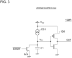
Wird ein Operationsverstärker einschließlich eines Differenzverstärkers als Spannungskomparator eingesetzt, so führt dies zu einem größeren Schaltungsumfang und einer höheren Leistungsaufnahme. In Anwendungen, die eine kleine Fläche und eine geringe Leistungsaufnahme erfordern, wird als ein solcher Spannungskomparator ein Inverter eingesetzt. Aus der
Die
In der
Außerdem kennt man noch die
ÜBERBLICKOVERVIEW
Die vorliegende Offenbarung wurde gemacht, um ein solches Problem zu lösen.The present disclosure has been made to solve such a problem.
Eine Ausführungsform der vorliegenden Offenbarung bezieht sich auf eine Zeitgeberschaltung. Die Zeitgeberschaltung umfasst: einen Kondensator; eine erste Stromquelle, die so strukturiert ist, dass sie den Kondensator auflädt; einen Inverter; eine zweite Stromquelle, die so strukturiert ist, dass sie einen Strom an einen Eingangsknoten des Inverters liefert; eine Stromspiegelschaltung, deren Ausgangsknoten mit dem Eingangsknoten des Inverters verbunden ist; und einen Widerstand, der zwischen einen Eingangsknoten der Stromspiegelschaltung und den Kondensator geschaltet ist.An embodiment of the present disclosure relates to a timing circuit. The timing circuit includes: a capacitor; a first current source structured to charge the capacitor; an inverter; a second current source structured to supply a current to an input node of the inverter; a current mirror circuit having an output node connected to the input node of the inverter; and a resistor connected between an input node of the current mirror circuit and the capacitor.
Mit der Spannung über dem Kondensator als VC1, mit der Schwellenspannung des eingangsseitigen Transistors der Stromspiegelschaltung als VTH und mit dem Widerstandswert des Widerstands als R1 wird der Strom I3, der durch den Widerstand und den Eingangsknoten der Stromspiegelschaltung fließt, durch I3 = (VC1 - VTH)/R1 dargestellt. Ist das Spiegelverhältnis der Stromspiegelschaltung K, so wird der Ausgangsstrom I4 der Stromspiegelschaltung durch I4 = K × I3 = K× (VC1 - VTH) /R1 dargestellt. Wird der von der zweiten Stromquelle erzeugte Strom I2 gleich dem Ausgangsstrom I4 der Stromspiegelschaltung, so ändert sich der Ausgang des Inverters. Dementsprechend wird die Kondensatorspannung VC1(TH) an dem Punkt, an dem sich der Ausgang des Inverters ändert, durch VC1(TH) = I2 × R1/K + VTH dargestellt. Die Spannung VC1(TH) ist ein konstanter Wert, der nicht von der Versorgungsspannung des Inverters abhängt. Dementsprechend ist eine solche Zeitgeberschaltung in der Lage, eine Zeitmessung ohne Abhängigkeit von der Versorgungsspannung durchzuführen.With the voltage across the capacitor as V C1 , the threshold voltage of the input transistor of the current mirror circuit as V TH and the resistance of the resistor as R1, the current I 3 flowing through the resistor and the input node of the current mirror circuit is represented by I 3 = (V C1 - V TH )/R1. If the mirror ratio of the current mirror circuit is K, the output current I 4 of the current mirror circuit is represented by I 4 = K × I 3 = K× (V C1 - V TH ) /R1. When the current I 2 generated by the second current source becomes equal to the output current I 4 of the current mirror circuit, the output of the inverter changes. Accordingly, the capacitor voltage V C1(TH) at the point where the output of the inverter changes is represented by V C1(TH) = I 2 × R1/K + V TH . The voltage V C1(TH) is a constant value that does not depend on the supply voltage of the inverter. Accordingly, such a timer circuit is able to perform a time measurement without dependence on the supply voltage.
In einer Ausführungsform kann die Stromspiegelschaltung unter Verwendung eines Feldeffekttransistors (FET) eingerichtet werden.In one embodiment, the current mirror circuit may be implemented using a field effect transistor (FET).
In einer Ausführungsform wird das Verhältnis zwischen der Kanalbreite W und der Kanallänge L, d.h. W/L, so bestimmt, dass bei einer Änderung des Ausgangs des Inverters eine Schwankung der Gate-Source-Spannung eines eingangsseitigen Transistors der Stromspiegelschaltung in einem Bereich von 0,1 V oder weniger oder, besonders bevorzugt, von 0,05 oder weniger in einem Fall, in dem eine Schwankung der Temperatur innerhalb eines garantierten Betriebstemperaturbereichs auftritt, gehalten wird. Dadurch lässt sich die Temperaturabhängigkeit der Messzeit verringern.In one embodiment, the ratio between the channel width W and the channel length L, i.e. W/L, is determined such that, when the output of the inverter changes, a fluctuation in the gate-source voltage of an input-side transistor of the current mirror circuit is kept within a range of 0.1 V or less, or, more preferably, 0.05 V or less in a case where a fluctuation in temperature occurs within a guaranteed operating temperature range. This makes it possible to reduce the temperature dependence of the measurement time.
In einer Ausführungsform kann die Stromspiegelschaltung unter Verwendung eines bipolaren Transistors eingerichtet werden.In one embodiment, the current mirror circuit may be implemented using a bipolar transistor.
In einer Ausführungsform kann die Zeitgeberschaltung monolithisch auf einem einzigen Halbleitersubstrat integriert sein. Beispiele für eine solche „integrierte“ Anordnung sind:
- eine Anordnung, bei der alle Schaltungskomponenten auf einem Halbleitersubstrat ausgebildet sind; und eine Anordnung, bei der die wichtigsten Schaltungskomponenten monolithisch integriert sind. Auch kann ein Teil der Schaltungskomponenten wie Widerstände oder Kondensatoren in Form von Komponenten außerhalb eines solchen Halbleitersubstrats angeordnet sein,
- um die Schaltungskonstanten anzupassen. Durch die Integration der Schaltung auf einem einzigen Chip ermöglicht eine solche Anordnung eine Verringerung der Schaltungsfläche und einheitliche Eigenschaften der Schaltungselemente.
- an arrangement in which all circuit components are formed on a semiconductor substrate; and an arrangement in which the main circuit components are monolithically integrated. Also, part of the circuit components such as resistors or capacitors can be arranged in the form of components outside such a semiconductor substrate,
- to adjust the circuit constants. By integrating the circuit on a single chip, such an arrangement enables a reduction in circuit area and uniform properties of the circuit elements.
Ein Oszillator gemäß einer Ausführungsform kann Folgendes umfassen: eine der oben beschriebenen Zeitgeberschaltungen; und eine Rücksetzschaltung, die so aufgebaut ist, dass sie den Kondensator als Reaktion auf den Ausgang des Inverters der Zeitgeberschaltung entlädt.An oscillator according to an embodiment may include: one of the timing circuits described above; and a reset circuit configured to discharge the capacitor in response to the output of the inverter of the timing circuit.
Ein Oszillator gemäß einer Ausführungsform kann zwei Zeitgeberschaltungen umfassen. Jede der beiden Zeitgeberschaltungen kann durch einen Ausgang der anderen Zeitgeberschaltung zurückgesetzt werden.An oscillator according to an embodiment may comprise two timer circuits. Each of the two timer circuits may be reset by an output of the other timer circuit.
Eine Halbleitervorrichtung gemäß einer Ausführungsform kann eine der oben beschriebenen Oszillatorschaltungen, eine durch ein Ausgangssignal der Oszillatorschaltung angesteuerte Ladungspumpenschaltung und einen N-Typ-Transistor enthalten, der so angeordnet ist, dass die Ausgangsspannung der Ladungspumpenschaltung über seine Steuerelektrode empfangen wird.A semiconductor device according to an embodiment may include one of the oscillator circuits described above, a charge pump circuit driven by an output signal of the oscillator circuit, and an N-type transistor arranged to receive the output voltage of the charge pump circuit via its control electrode.
KURZBESCHREIBUNG DER ZEICHNUNGSFIGURENSHORT DESCRIPTION OF THE DRAWING FIGURES
Die Ausführungsformen werden hier nur beispielhaft unter Bezugnahme auf die beigefügten Zeichnungsfiguren beschrieben, die beispielhaft und nicht einschränkend sein sollen, und in denen gleiche Elemente in mehreren Figuren gleich nummeriert sind:
-
1 ist ein Schaltplan einer Zeitgeberschaltung gemäß einer Ausführungsform; -
2 ist ein Betriebswellenformdiagramm der in1 gezeigten Zeitgeberschaltung; -
3 ist ein Schaltplan einer Zeitgeberschaltung gemäß einer Vergleichstechnik; -
4 ist ein Schaltplan eines Oszillators gemäß einer Ausführungsform; -
5 ist ein Betriebswellenformdiagramm des in4 gezeigten Oszillators; -
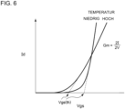
6 ist eine schematische Ansicht zur Erläuterung der Temperatureigenschaften eines MOSFETs; -
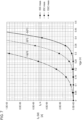
7 ist eine Ansicht, die die Spannungs-Strom-Kennlinien eines eingangsseitigen Transistors in einem Fall zeigt, in dem der eingangsseitige Transistor eine ungeeignete Größe hat; -
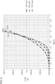
8 ist eine Ansicht, die die Spannungs-Strom-Kennlinien des eingangsseitigen Transistors mit optimierter Größe zeigt; -
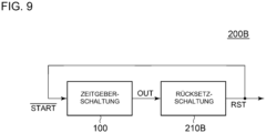
9 ist ein Schaltplan eines Oszillators gemäß einer Modifikation; -
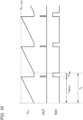
10 ist ein Betriebswellenformdiagramm des in9 gezeigten Oszillators; und -
11 ist ein Schaltplan einer Halbleitervorrichtung mit einem Oszillator.
-
1 is a circuit diagram of a timer circuit according to an embodiment; -
2 is an operating waveform diagram of the1 timer circuit shown; -
3 is a circuit diagram of a timer circuit according to a comparative technique; -
4 is a circuit diagram of an oscillator according to an embodiment; -
5 is an operating waveform diagram of the4 shown oscillator; -
6 is a schematic view explaining the temperature characteristics of a MOSFET; -
7 is a view showing the voltage-current characteristics of an input-side transistor in a case where the input-side transistor has an inappropriate size; -
8 is a view showing the voltage-current characteristics of the input-side transistor with optimized size; -
9 is a circuit diagram of an oscillator according to a modification; -
10 is an operating waveform diagram of the9 shown oscillator; and -
11 is a circuit diagram of a semiconductor device with an oscillator.
DETAILLIERTE BESCHREIBUNGDETAILED DESCRIPTION
Es folgt ein Überblick über mehrere beispielhafte Ausführungsformen der Offenbarung. Dieser Überblick dient dem Zweck, dem Leser ein grundlegendes Verständnis solcher Ausführungsformen zu vermitteln, und definiert den Offenbarungsumfang nicht vollständig. Dieser Überblick ist kein umfassender Überblick über alle in Betracht gezogenen Ausführungsformen und soll weder Schlüssel- oder kritische Elemente aller Ausführungsformen identifizieren noch den Umfang eines oder aller Aspekte abgrenzen. Sein einziger Zweck ist es, einige Konzepte einer oder mehrerer Ausführungsformen in vereinfachter Form als Auftakt für die spätere detailliertere Beschreibung vorzustellen. Der Einfachheit halber kann der Begriff „eine Ausführungsform“ hier verwendet werden, um sich auf eine einzelne Ausführungsform oder mehrere Ausführungsformen der Offenbarung zu beziehen.The following is an overview of several exemplary embodiments of the disclosure. This overview is intended to provide the reader with a basic understanding of such embodiments and does not fully define the scope of the disclosure. This overview is not a comprehensive overview of all contemplated embodiments and is not intended to identify key or critical elements of all embodiments, nor to delimit the scope of any or all aspects. Its sole purpose is to introduce some concepts of one or more embodiments in a simplified form as a prelude to the more detailed description later. For convenience, the term "an embodiment" may be used herein to refer to a single embodiment or multiple embodiments of the disclosure.
AUSFÜHRUNGSFORMENEMBODIMENTS
Im Folgenden werden bevorzugte Ausführungsformen unter Bezugnahme auf die Zeichnungsfiguren beschrieben. Gleiche oder ähnliche Bauteile, Elemente und Verfahren sind mit den gleichen Bezugsziffern bezeichnet, und eine redundante Beschreibung wird gegebenenfalls weggelassen. Die Ausführungsformen wurden nur für beispielhafte Zwecke beschrieben und sollen keineswegs die vorliegende Offenbarung und die vorliegende Erfindung einschränken. Auch ist es für die vorliegende Offenbarung und die vorliegende Erfindung nicht notwendigerweise erforderlich, dass alle Merkmale oder eine Kombination davon wie in den Ausführungsbeispielen beschrieben bereitgestellt werden.In the following, preferred embodiments are described with reference to the drawing figures. The same or similar components, elements and processes are designated by the same reference numerals, and redundant description is omitted where appropriate. The embodiments have been described for exemplary purposes only and are in no way intended to limit the present disclosure and the present invention. Nor is it necessarily required for the present disclosure and the present invention that all features or a combination thereof be provided as described in the embodiments.
In einigen Fällen sind die Größen (Dicke, Länge, Breite usw.) der einzelnen in den Zeichnungsfiguren dargestellten Komponenten zum besseren Verständnis erweitert (vergrößert) oder reduziert. Das Größenverhältnis zwischen mehreren Komponenten in den Zeichnungsfiguren entspricht nicht unbedingt dem tatsächlichen Größenverhältnis zwischen ihnen. Das heißt, dass selbst in einem Fall, in dem ein bestimmtes Bauteil A eine größere Dicke als ein anderes Bauteil B in den Zeichnungsfiguren aufweist, in einigen Fällen das Bauteil A in Wirklichkeit eine geringere Dicke als das Bauteil B hat.In some cases, the sizes (thickness, length, width, etc.) of individual components shown in the drawing figures are expanded (magnified) or reduced for ease of understanding. The size relationship between several components in the drawing figures does not necessarily correspond to the actual size relationship between them. That is, even in a case where a certain component A has a greater thickness than another component B in the drawing figures, in some cases the component A actually has a smaller thickness than the component B.
In der vorliegenden Beschreibung schließt ein Zustand, der durch die Formulierung „das Element A ist mit dem Element B gekoppelt“ dargestellt wird, einen Zustand ein, in dem das Element A indirekt mit dem Element B über ein anderes Element gekoppelt ist, das die elektrische Verbindung zwischen ihnen nicht wesentlich beeinträchtigt, oder das die Funktionen oder Wirkungen der Verbindung zwischen ihnen nicht beschädigt, zusätzlich zu einem Zustand, in dem sie physisch und direkt gekoppelt sind.In the present specification, a state represented by the phrase "element A is coupled to element B" includes a state in which element A is indirectly coupled to element B via another element that does not substantially impair the electrical connection between them or that does not damage the functions or effects of the connection between them, in addition to a state in which they are physically and directly coupled.
In ähnlicher Weise umfasst ein Zustand, der durch die Formulierung „das Element C ist zwischen dem Element A und dem Element B vorgesehen“ dargestellt wird, einen Zustand, in dem das Element A indirekt mit dem Element C gekoppelt ist oder das Element B indirekt mit dem Element C über ein anderes Element gekoppelt ist, das die elektrische Verbindung zwischen ihnen nicht wesentlich beeinträchtigt oder die Funktionen oder Wirkungen der Verbindung zwischen ihnen nicht beeinträchtigt, zusätzlich zu einem Zustand, in dem sie direkt gekoppelt sind. In der vorliegenden Beschreibung stellen diejenigen Bezugssymbole, die elektrische Signale wie ein Spannungssignal, ein Stromsignal oder dergleichen bezeichnen, und die Bezugssymbole, die Schaltungselemente wie einen Widerstand, einen Kondensator, eine Induktivität oder dergleichen bezeichnen, je nach Bedarf auch den entsprechenden Spannungswert, Stromwert oder Schaltungskonstanten (Widerstandswert, Kapazitätswert, Induktivität) dar.Similarly, a state represented by the phrase "element C is provided between element A and element B" includes a state in which element A is indirectly coupled to element C or element B is indirectly coupled to element C through another element that does not substantially affect the electrical connection between them or does not affect the functions or effects of the connection between them, in addition to a state in which they are directly coupled. In the present specification, those reference symbols denoting electrical signals such as a voltage signal, a current signal, or the like, and the reference symbols denoting circuit elements such as a resistor, a capacitor, an inductance, or the like also represent the corresponding voltage value, current value, or circuit constant (resistance value, capacitance value, inductance), as appropriate.
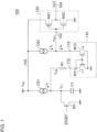
Die Zeitgeberschaltung 100 enthält einen Kondensator C1, eine erste Stromquelle CS1, eine zweite Stromquelle CS2, eine Stromspiegelschaltung 110, einen Widerstand R1, einen Inverter 120 und einen Rücksetztransistor M3. Eine Stromversorgungsspannung VDD wird an eine Stromversorgungsleitung 102 der Zeitgeberschaltung 100 angelegt.The
Der Kondensator C1 ist so angeordnet, dass ein Ende geerdet ist. Die erste Stromquelle CS1 ist mit dem anderen Ende des Kondensators C1 verbunden. Die erste Stromquelle CS1 dient als Quelle eines konstanten Stroms I1 zum Kondensator C1, um den Kondensator C1 zu laden.The capacitor C1 is arranged so that one end is grounded. The first current source CS1 is connected to the other end of the capacitor C1. The first current source CS1 serves as a source a constant current I 1 to the capacitor C1 to charge the capacitor C1.
Der Inverter 120 umfasst einen High-Side-Transistor M21 und einen Low-Side-Transistor M22, die zwischen der Stromversorgungsleitung 102 und der Masse geschaltet sind. Insbesondere ist der High-Side-Transistor M21 zwischen der Stromversorgungsleitung 102 und der Ausgangsleitung 104 verbunden. Der Low-Side-Transistor M22 ist zwischen die Ausgangsleitung 104 und die Masse geschaltet.The
Die zweite Stromquelle CS2 ist mit einem Eingangsknoten 122 des Inverters 120 verbunden. Die zweite Stromquelle CS2 fungiert als Quelle eines Stroms I2 zum Eingangsknoten des Inverters 120.The second current source CS2 is connected to an
Die Stromspiegelschaltung 110 spiegelt den Strom, der durch den Eingangsknoten 112 fließt, auf eine Weise, dass er mit K multipliziert wird („K“ wird als Spiegelverhältnis bezeichnet), und dass der gespiegelte Strom zurückgefaltet und von einem Ausgangsknoten 114 abgesenkt wird. Die Stromspiegelschaltung 110 umfasst einen eingangsseitigen Transistor M11 und einen ausgangsseitigen Transistor M12. Der Ausgangsknoten 114 der Stromspiegelschaltung 110 ist mit dem Eingangsknoten 122 des Inverters 120 verbunden.The
Der Widerstand R1 ist zwischen dem Eingangsknoten 112 der Stromspiegelschaltung 110 und dem Kondensator C1 angeschlossen.The resistor R1 is connected between the
Der Rücksetz-Transistor M3 (auch: Reset-Transistor M3) ist mit dem Kondensator C1 parallel geschaltet. Während einer Zeitspanne, in der das Startsignal /START negiert (high) ist, wird der Reset-Transistor M3 eingeschaltet, um den Kondensator C1 zu entladen. Während einer Zeitspanne, in der das Startsignal /START aktiviert (low) ist, wird der Reset-Transistor M3 derart ausgeschaltet, dass der Kondensator C1 mit Hilfe der ersten Stromquelle CS1 geladen werden kann.The reset transistor M3 is connected in parallel with the capacitor C1. During a period in which the start signal /START is negated (high), the reset transistor M3 is switched on to discharge the capacitor C1. During a period in which the start signal /START is activated (low), the reset transistor M3 is switched off in such a way that the capacitor C1 can be charged using the first current source CS1.
Die obige Darstellung zeigt den Aufbau der Zeitgeberschaltung 100. Nachfolgend wird ihre Funktionsweise beschrieben.The above illustration shows the structure of the
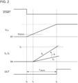
Vor dem Zeitpunkt t0 wird das Startsignal /START negiert, und der Reset-Transistor M3 wird eingeschaltet. In diesem Zustand ist die Kondensatorspannung VC1 auf 0 V festgelegt.Before time t 0 , the start signal /START is negated and the reset transistor M3 is turned on. In this state, the capacitor voltage V C1 is fixed at 0 V.
Wenn das Startsignal /START zum Zeitpunkt t0 anliegt, wird der Kondensator C1 durch den von der ersten Stromquelle CS1 erzeugten Strom I1 aufgeladen. Damit steigt die Kondensatorspannung VC1 mit der Zeit an.When the start signal /START is applied at time t 0 , the capacitor C1 is charged by the current I 1 generated by the first current source CS1. Thus, the capacitor voltage V C1 increases over time.
Überschreitet die Kondensatorspannung VC1 eine Gate-Source-Schwellenspannung VGS(th) des eingangsseitigen Transistors M11 der Stromspiegelschaltung 110, so beginnt der Strom I3 durch den Widerstand R1 und die Eingangsseite der Stromspiegelschaltung 110 zu fließen. Der Strom I3 wird durch die folgende Gleichung dargestellt.![]()
![]()
Zur Vereinfachung der Beschreibung zeigt
Vor dem Zeitpunkt t2 gilt die Beziehung I4 < I2. Dementsprechend ist die Spannung VINV des Eingangsknotens 122 des Inverters 120 hoch (VDD). Dementsprechend ist der Ausgang des Inverters 120, d. h. der Ausgang OUT der Zeitgeberschaltung 100, niedrig.Before time t 2 , the relationship I 4 < I 2 holds. Accordingly, the voltage V INV of the
Übersteigt der Strom I4 den Strom I2 (I1 > I2) zum Zeitpunkt t3, so wird die Spannung VINV des Eingangsknotens 122 des Inverters 120 auf niedrig (0 V) gesetzt. In diesem Zustand geht der Ausgang des Inverters 120, d. h. der Ausgang OUT der Zeitgeberschaltung 100, auf High.If the current I 4 exceeds the current I 2 (I 1 > I 2 ) at time t 3 , the voltage V INV of the
Die Zeit zwischen den Zeitpunkten t0 und t2 wird von der Zeitgeberschaltung 100 als Messzeit τMEAS verwendet. Die Kondensatorspannung VC1(TH) zum Zeitpunkt t2 wird durch VC1(TH) = I2× R1/K + VC1(TH) dargestellt.The time between times t 0 and t 2 is used by the
Mit Blick auf den Kondensator C1 wird die Kondensatorspannung VC1 durch Aufladen des Kondensators C1 mit einem Ladestrom ICHG = I1 - I3 erzeugt. Dementsprechend ist die Integrationszeit τ dargestellt durch C1 × (I2× R1/K + VC1(TH)) =∫τ ICHG (t) dt die Messzeit τMEAS.With regard to the capacitor C1, the capacitor voltage V C1 is generated by charging the capacitor C1 with a charging current I CHG = I 1 - I 3 . Accordingly, the integration time τ represented by C1 × (I 2 × R1/K + V C1(TH) ) =∫ τ I CHG (t) dt the measurement time τ MEAS .
Die obigen Ausführungen beschreiben die Funktionsweise der Zeitschaltung 100. Die Vorteile der Timer-Schaltung 100 können im Vergleich zu herkömmlichen Techniken klar verstanden werden.The above describes the operation of the
Der Kondensator C1 wird durch den von der Stromquelle CS1 erzeugten Strom I1 geladen. Die Kondensatorspannung VC1 steigt mit einer konstanten Steigung mit der Zeit an. Erreicht die Kondensatorspannung VC1 die Schwellenspannung des Inverters 120, so wechselt der Ausgang OUT von High zu Low.The capacitor C1 is charged by the current I 1 generated by the current source CS1. The capacitor voltage V C1 increases with a constant slope over time. When the capacitor voltage V C1 reaches the threshold voltage of the
Dabei ist die Schwellenspannung des Inverters 120 die Hälfte der Versorgungsspannung VDD. Dementsprechend führt bei der in
Als nächstes wird die Verwendung der Zeitgeberschaltung 100 beschrieben. Die Zeitgeberschaltung 100 kann in einer Oszillatorschaltung verwendet werden.Next, the use of the
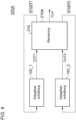
Die erste Zeitgeberschaltung 100_1 und die zweite Zeitgeberschaltung 100_2 haben jeweils die gleiche Konfiguration wie die oben beschriebene Zeitgeberschaltung 100. Die jeweiligen Messzeiten τMEAS1 und τMEAS2 der ersten Zeitgeberschaltung 100_1 und der zweiten Zeitgeberschaltung 100_2 können gleich oder unterschiedlich sein.The first timer circuit 100_1 and the second timer circuit 100_2 each have the same configuration as the
Die Steuerschaltung 210 setzt ein zweites Startsignal /START2 für die zweite Zeitgeberschaltung 100_2 in Reaktion auf die Aktivierung eines Ausgangs OUT1 der ersten Zeitgeberschaltung 100_1 durch. Außerdem setzt die Steuerschaltung 210 ein erstes Startsignal /START1 für die erste Zeitgeberschaltung 100_1 in Reaktion auf die Aktivierung eines Ausgangs OUT2 der zweiten Zeitgeberschaltung 100_2 durch. Während einer Zeitspanne, in der entweder das erste Startsignal /START1 oder das zweite Startsignal /START2 aktiviert ist, wird ein Ausgang CLK der Steuerung 210 auf einen ersten Pegel (z.B. High) gesetzt. Während einer Zeitspanne, in der das andere Signal anliegt, wird der Ausgang CLK der Steuerung 210 auf einen zweiten Pegel (z. B. low) gesetzt.The
Als Nächstes werden die Temperatureigenschaften der Zeitgeberschaltung 100 beschrieben. Die Messzeit τMEAS der Zeitgeberschaltung 100 wird durch die Temperatureigenschaften der Stromspiegelschaltung 110 beeinflusst.Next, the temperature characteristics of the
Ein MOSFET hat die folgenden Eigenschaften.
- (i) Mit zunehmender Temperatur wird die Gate-Source-Schwellenspannung VGS(th) des MOSFET niedriger, was dazu führt, dass der Drainstrom leicht fließt. In
6 ist VGS(th) als eine mit der Gmmax-Methode ermittelte Spannung dargestellt. (ii) Mit zunehmender Temperatur wird der Leitwert Gm des MOSFET, d. h. die Steigung des Drainstroms Id im Verhältnis zur Gate-Spannung Vgs (dId/dVgs), kleiner.
- (i) As the temperature increases, the gate-source threshold voltage V GS(th) of the MOSFET becomes lower, which causes the drain current to flow easily. In
6 V GS(th) is represented as a voltage determined by the Gmmax method. (ii) As the temperature increases, the conductance Gm of the MOSFET, ie the slope of the drain current Id with respect to the gate voltage Vgs (dId/dVgs), decreases.
Entsprechend kann vorzugsweise der Arbeitspunkt des eingangsseitigen Transistors M11 der Stromspiegelschaltung 110 (Gate-Source-Spannung, d.h. die Gate-Drain-Spannung, d.h. die Spannung am Eingangsknoten 112 der Stromspiegelschaltung 110) bestimmt werden. Weiterhin kann das Verhältnis zwischen der Kanalbreite W und der Kanallänge L des eingangsseitigen Transistors M11, also W/L, vorzugsweise so bestimmt werden, dass sich die in (i) beschriebenen Temperaturkennlinien und die in (ii) beschriebenen Temperaturkennlinien gegenseitig aufheben.Accordingly, the operating point of the input-side transistor M11 of the current mirror circuit 110 (gate-source voltage, i.e. the gate-drain voltage, i.e. the voltage at the
So kann beispielsweise die Gate-Source-Spannung Vgs des eingangsseitigen Transistors zu einem Zeitpunkt, an dem sich der Ausgang des Inverters 120 ändert, innerhalb einer Schwankung von 0,1 V oder weniger, vorzugsweise 0,05 V oder weniger, gesteuert werden, wenn sich die Temperatur innerhalb des garantierten Betriebstemperaturbereichs ändert.For example, the gate-source voltage Vgs of the input-side transistor at a time when the output of the
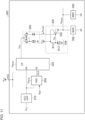
Man beachte, dass die Konfiguration des Oszillators 200 mit der Zeitgeberschaltung 100 nicht auf die in
Eine externe Stromversorgungsspannung VCC wird von einer externen Stromversorgungsschaltung an einen Stromversorgungsanschluss VCC der Halbleitervorrichtung 300 geliefert. Die Reglerschaltung 330 empfängt die externe Versorgungsspannung VCC als Eingangsspannung und erzeugt eine interne Versorgungsspannung VREG5, die auf einen vorbestimmten Zielpegel (z. B. 5 V) stabilisiert ist. Die interne Versorgungsspannung VREG5 wird an Lastschaltungen wie die Referenzstromquelle 350, die Bandlücken-Bezugsschaltung 352 usw. geliefert.An external power supply voltage V CC is supplied from an external power supply circuit to a power supply terminal V CC of the
Die Reglerschaltung 330 ist als Source-Folger-Schaltung mit einem NMOS-Transistor 332 und einer Vorspannungsschaltung 334 eingerichtet. Die Vorspannungsschaltung 334 umfasst eine Zenerdiode DLZ und einen Widerstand R11. Die Vorspannungsschaltung 334 erzeugt eine Zener-Spannung Vz der Zener-Diode DLZ am Gate des NMOS-Transistors 332. Die interne Versorgungsspannung VREG5 wird auf einen Zielwert stabilisiert, der durch VREF (REF) = VZ - VGS dargestellt wird. VGS steht dabei für die Gate-Source-Spannung des NMOS-Transistors 332. Die Zener-Spannung Vz wird beispielsweise so festgelegt, dass VREF (REF) = 5 V gilt.The
Ist die externe Versorgungsspannung VCC niedriger ist als der Sollwert (5 V) der internen Versorgungsspannung VREG5, d. h. die Zener-Spannung Vz der Zener-Diode DLZ, so kann die Vorspannungsschaltung 334 nicht arbeiten. Um den NMOS-Transistor 332 in diesem Zustand in geeigneter Weise vorzuspannen, sind die UVP-Schaltung 310, der Oszillator 200 und die Ladungspumpenschaltung 320 vorgesehen.If the external supply voltage V CC is lower than the set value (5 V) of the internal supply voltage V REG5 , ie the Zener voltage Vz of the Zener diode DLZ, the
Die UVP-Schaltung 310 vergleicht die externe Versorgungsspannung VCC mit einem Unterspannungs-schwellenwert VUVP . Wenn VCC > VUVP gilt, setzt die UVP-Schaltung 310 das UVP-Signal durch (z. B. auf High).The
Wird das UVP-Signal aktiviert, so geht der Oszillator 200 in den Betriebszustand über. In diesem Zustand erzeugt der Oszillator 200 ein Taktsignal CLK. Außerdem wird das UVP-Signal einem Freigabeanschluss der Ladungs-pumpenschaltung 320 zugeführt. Wird das UVP-Signal aktiviert, so geht die Ladungspumpenschaltung 320 in den Freigabezustand über. In diesem Zustand erhöht die Ladungspumpenschaltung 320 die interne Stromversorgungsspannung VREG5 synchron mit dem Taktsignal CLK, um die Ladungspumpenspannung VCP zu erzeugen. Die Ladungspumpenspannung VCP ist höher als der Sollpegel der internen Stromversorgungsspannung VREG5 .If the UVP signal is activated, the
Die Einschaltvorspannungsschaltung 340 arbeitet mit der Ladungspumpenspannung VCP als Stromversorgung. Die Einschaltvorspannungsschaltung 340 fungiert als Quelle des Einschaltstroms ISTART zum Gate des NMOS-Transistors 332. Mit einer solchen Anordnung, bei der der Anlaufstrom ISTART durch die Zener-Diode DLZ fließt, ist diese in der Lage, die Zener-Spannung Vz am Gate des NMOS-Transistors 332 auch in einem Zustand zu erzeugen, in dem die externe Versorgungsspannung VCC niedrig ist.The turn-on
Bei einer solchen Anordnung, bei der der Oszillator 200 zur Lieferung des Taktsignals CLK an die Ladungspumpenschaltung 320 unter Verwendung der Zeitgeberschaltung 100 gemäß der vorliegenden Ausführungsform eingerichtet ist, ist diese in der Lage, das Taktsignal CLK mit einer stabilen Frequenz zu erzeugen.With such an arrangement, where the
MODIFIKATIONENMODIFICATIONS
In der Ausführungsform wurde eine Anordnung beschrieben, bei der die Stromspiegelschaltung 110 mit MOSFETs eingerichtet ist. Die Stromspiegelschaltung 110 kann jedoch auch mit bipolaren Transistoren eingerichtet werden. Die anderen Schaltungsblöcke als die Stromspiegelschaltung 110, z. B. der Inverter 120, der Rücksetztransistor M3, die erste Stromquelle CS1, die zweite Stromquelle CS2 oder ähnliches, können mit bipolaren Transistoren eingerichtet werden.In the embodiment, a configuration in which the
Die vorliegende Erfindung wurde unter Bezugnahme auf die Ausführungsformen mit spezifischen Begriffen beschrieben. Allerdings zeigen die oben beschriebenen Ausführungsformen nur einen Aspekt der Mechanismen und Anwendungen der vorliegenden Erfindung. Vielmehr können verschiedene Modifikationen und verschiedene Änderungen in der Anordnung vorgenommen werden, ohne von Erfindungsidee oder Schutzumfang der vorliegenden Erfindung, die in den beigefügten Ansprüchen definiert ist, abzuweichen.The present invention has been described with reference to the embodiments in specific terms. However, the embodiments described above show only one aspect of the mechanisms and applications of the present invention. Rather, various modifications and various changes in arrangement can be made without departing from the spirit or scope of the present invention which is defined in the appended claims.
Claims (9)
Applications Claiming Priority (2)
| Application Number | Priority Date | Filing Date | Title |
|---|---|---|---|
| JP2022102126A JP2024002737A (en) | 2022-06-24 | 2022-06-24 | Timer circuits, oscillator circuits, semiconductor devices |
| JP2022-102126 | 2022-06-24 |
Publications (2)
| Publication Number | Publication Date |
|---|---|
| DE102023116552A1 DE102023116552A1 (en) | 2024-01-04 |
| DE102023116552B4 true DE102023116552B4 (en) | 2025-02-06 |
Family
ID=89167522
Family Applications (1)
| Application Number | Title | Priority Date | Filing Date |
|---|---|---|---|
| DE102023116552.6A Expired - Fee Related DE102023116552B4 (en) | 2022-06-24 | 2023-06-23 | TIMER CIRCUIT, OSCILLATOR CIRCUIT AND SEMICONDUCTOR DEVICE |
Country Status (3)
| Country | Link |
|---|---|
| US (1) | US12348226B2 (en) |
| JP (1) | JP2024002737A (en) |
| DE (1) | DE102023116552B4 (en) |
Citations (4)
| Publication number | Priority date | Publication date | Assignee | Title |
|---|---|---|---|---|
| JP2003085972A (en) | 2001-09-13 | 2003-03-20 | Toshiba Corp | Timer circuit and semiconductor memory device |
| EP1693960A1 (en) | 2005-02-18 | 2006-08-23 | STMicroelectronics S.r.l. | Electronic circuit and oscillator comprising said electronic circuit |
| US20080290955A1 (en) | 2007-05-24 | 2008-11-27 | Atmel Corporation | Low cost and low variation oscillator |
| US20100201454A1 (en) | 2009-02-09 | 2010-08-12 | Yi-Tzu Chen | VDD-Independent Oscillator Insensitive to Process Variation |
Family Cites Families (1)
| Publication number | Priority date | Publication date | Assignee | Title |
|---|---|---|---|---|
| JP5621673B2 (en) * | 2011-03-18 | 2014-11-12 | 富士通セミコンダクター株式会社 | Detection circuit |
-
2022
- 2022-06-24 JP JP2022102126A patent/JP2024002737A/en active Pending
-
2023
- 2023-06-08 US US18/331,495 patent/US12348226B2/en active Active
- 2023-06-23 DE DE102023116552.6A patent/DE102023116552B4/en not_active Expired - Fee Related
Patent Citations (4)
| Publication number | Priority date | Publication date | Assignee | Title |
|---|---|---|---|---|
| JP2003085972A (en) | 2001-09-13 | 2003-03-20 | Toshiba Corp | Timer circuit and semiconductor memory device |
| EP1693960A1 (en) | 2005-02-18 | 2006-08-23 | STMicroelectronics S.r.l. | Electronic circuit and oscillator comprising said electronic circuit |
| US20080290955A1 (en) | 2007-05-24 | 2008-11-27 | Atmel Corporation | Low cost and low variation oscillator |
| US20100201454A1 (en) | 2009-02-09 | 2010-08-12 | Yi-Tzu Chen | VDD-Independent Oscillator Insensitive to Process Variation |
Also Published As
| Publication number | Publication date |
|---|---|
| US20230421140A1 (en) | 2023-12-28 |
| US12348226B2 (en) | 2025-07-01 |
| JP2024002737A (en) | 2024-01-11 |
| DE102023116552A1 (en) | 2024-01-04 |
Similar Documents
| Publication | Publication Date | Title |
|---|---|---|
| DE69422239T2 (en) | Reference voltage generator circuit | |
| DE3782367T2 (en) | MOS SEMICONDUCTOR CIRCUIT. | |
| DE69319294T2 (en) | Temperature and supply voltage independent oscillator with low consumption | |
| DE69408665T2 (en) | Voltage pump type voltage booster | |
| DE69122541T2 (en) | Static switch for medium voltage | |
| EP0587938B1 (en) | Integrated buffer circuit | |
| DE69408320T2 (en) | DEVICE AND METHOD FOR ADJUSTING THE THRESHOLD VOLTAGE OF MOS TRANSISTORS | |
| DE3419661C2 (en) | ||
| DE10348364B4 (en) | Oscillator circuit with stable frequency | |
| DE4037206A1 (en) | SOURCE VOLTAGE CONTROL CIRCUIT | |
| DE69320505T2 (en) | Automatic reset circuit with improved testability | |
| DE10152285A1 (en) | Function generator with adjustable vibration frequency | |
| DE102006003123B4 (en) | Reference voltage circuits | |
| DE19725459B4 (en) | External voltage independent reverse bias level detector | |
| DE102024111286A1 (en) | switching regulator with low-energy single-rail architecture | |
| DE69111869T2 (en) | Reference voltage generation circuit. | |
| DE102005043376B4 (en) | Oscillator arrangement and method for generating a periodic signal | |
| DE69031751T2 (en) | Integrated semiconductor circuit with an intrinsic MOS transistor for generating a reference voltage | |
| DE102016221863B4 (en) | Switching power supply | |
| DE4201516A1 (en) | DEVICE FOR AUTOMATICALLY TESTING A STRENGTH OPERATION OF A SEMICONDUCTOR STORAGE DEVICE | |
| EP1494038B1 (en) | Method and device for the determination of the ratio of a RC time constant in an integrated circuit to a set value | |
| DE4038319C2 (en) | Circuit for generating a reference voltage which can be increased for test purposes in order to burn in an integrated circuit | |
| DE69125465T2 (en) | Fast driver circuit for capacitive load, especially for ICs and for memory | |
| DE69413793T2 (en) | Power source | |
| DE102023116552B4 (en) | TIMER CIRCUIT, OSCILLATOR CIRCUIT AND SEMICONDUCTOR DEVICE |
Legal Events
| Date | Code | Title | Description |
|---|---|---|---|
| R012 | Request for examination validly filed | ||
| R016 | Response to examination communication | ||
| R018 | Grant decision by examination section/examining division | ||
| R020 | Patent grant now final | ||
| R119 | Application deemed withdrawn, or ip right lapsed, due to non-payment of renewal fee |