DE102018009850A1 - Stack-shaped multiple solar cell - Google Patents
Stack-shaped multiple solar cell Download PDFInfo
- Publication number
- DE102018009850A1 DE102018009850A1 DE102018009850.9A DE102018009850A DE102018009850A1 DE 102018009850 A1 DE102018009850 A1 DE 102018009850A1 DE 102018009850 A DE102018009850 A DE 102018009850A DE 102018009850 A1 DE102018009850 A1 DE 102018009850A1
- Authority
- DE
- Germany
- Prior art keywords
- layer
- solar cell
- tunnel diode
- multiple solar
- sub
- Prior art date
- Legal status (The legal status is an assumption and is not a legal conclusion. Google has not performed a legal analysis and makes no representation as to the accuracy of the status listed.)
- Granted
Links
Images


Classifications
-
- H—ELECTRICITY
- H10—SEMICONDUCTOR DEVICES; ELECTRIC SOLID-STATE DEVICES NOT OTHERWISE PROVIDED FOR
- H10F—INORGANIC SEMICONDUCTOR DEVICES SENSITIVE TO INFRARED RADIATION, LIGHT, ELECTROMAGNETIC RADIATION OF SHORTER WAVELENGTH OR CORPUSCULAR RADIATION
- H10F10/00—Individual photovoltaic cells, e.g. solar cells
- H10F10/10—Individual photovoltaic cells, e.g. solar cells having potential barriers
- H10F10/16—Photovoltaic cells having only PN heterojunction potential barriers
- H10F10/161—Photovoltaic cells having only PN heterojunction potential barriers comprising multiple PN heterojunctions, e.g. tandem cells
-
- H—ELECTRICITY
- H10—SEMICONDUCTOR DEVICES; ELECTRIC SOLID-STATE DEVICES NOT OTHERWISE PROVIDED FOR
- H10F—INORGANIC SEMICONDUCTOR DEVICES SENSITIVE TO INFRARED RADIATION, LIGHT, ELECTROMAGNETIC RADIATION OF SHORTER WAVELENGTH OR CORPUSCULAR RADIATION
- H10F10/00—Individual photovoltaic cells, e.g. solar cells
- H10F10/10—Individual photovoltaic cells, e.g. solar cells having potential barriers
- H10F10/16—Photovoltaic cells having only PN heterojunction potential barriers
- H10F10/163—Photovoltaic cells having only PN heterojunction potential barriers comprising only Group III-V materials, e.g. GaAs/AlGaAs or InP/GaInAs photovoltaic cells
-
- Y—GENERAL TAGGING OF NEW TECHNOLOGICAL DEVELOPMENTS; GENERAL TAGGING OF CROSS-SECTIONAL TECHNOLOGIES SPANNING OVER SEVERAL SECTIONS OF THE IPC; TECHNICAL SUBJECTS COVERED BY FORMER USPC CROSS-REFERENCE ART COLLECTIONS [XRACs] AND DIGESTS
- Y02—TECHNOLOGIES OR APPLICATIONS FOR MITIGATION OR ADAPTATION AGAINST CLIMATE CHANGE
- Y02E—REDUCTION OF GREENHOUSE GAS [GHG] EMISSIONS, RELATED TO ENERGY GENERATION, TRANSMISSION OR DISTRIBUTION
- Y02E10/00—Energy generation through renewable energy sources
- Y02E10/50—Photovoltaic [PV] energy
- Y02E10/544—Solar cells from Group III-V materials
Landscapes
- Photovoltaic Devices (AREA)
Abstract
Die Erfindung betrifft eine stapelförmige monolithische aufrecht Mehrfachsolarzelle aufweisend mindestens eine erste Teilzelle mit einer ersten Bandlücke , einer ersten Gitterkonstante und zu mehr als 50% aus Germanium bestehend, eine über der ersten Teilzelle angeordnete zweite Teilzelle mit einer zweiten Bandlücke und einer zweiten Gitterkonstante, einen zwischen der ersten Teilzelle und der zweiten Teilzelle eine erste Tunneldiode mit einer n+-Schicht und eine p+-Schicht angeordnet ist, wobei die zweite Bandlücke größer als die erste Bandlücke ist, die n+-Schicht der ersten Tunneldiode InGaP umfasst, die p+-Schicht der ersten Tunneldiode ein As-haltiges III-V Material umfasst, zwischen der n+-Schicht und der p+-Schicht eine Zwischenschicht angeordnet ist und die Zwischenschicht jeweils dünner ist als die n+-Schicht und als die p+-Schicht.
Description
Die Erfindung betrifft eine stapelförmige Mehrfachsolarzelle.The invention relates to a stack-shaped multiple solar cell.
Ein monolithischer Solarzellenstapel ist aus
Aus der
Eine tensil verspannte entartete Schicht ist mit einer kompressiv verspannten entarteten Schicht kompensiert. Die entarteten Schichten sind entweder als mit Kohlenstoff dotierte entartete p+- oder als mit Tellur oder Silizium dotierte entartete n+-Schichten ausgeführt. Indem die Verspannung kompensiert ist, wirkt keine Verspannung auf die die Tunneldiode umgebenden Schichten, anders ausgedrückt die Summe der Verspannung ist null.A tensile strained degenerate layer is compensated with a compressively strained degenerate layer. The degenerate layers are designed either as degenerate p + doped with carbon or as degenerate n + layers doped with tellurium or silicon. By compensating the tension, no tension acts on the layers surrounding the tunnel diode, in other words the sum of the tension is zero.
Vor diesem Hintergrund besteht die Aufgabe der Erfindung darin, eine Vorrichtung anzugeben, die den Stand der Technik weiterbildet.Against this background, the object of the invention is to provide a device which further develops the prior art.
Die Aufgabe wird durch eine Mehrfachsolarzelle mit den Merkmalen des Patentanspruchs 1 gelöst. Vorteilhafte Ausgestaltungen der Erfindung sind Gegenstand von Unteransprüchen.The object is achieved by a multiple solar cell with the features of patent claim 1. Advantageous embodiments of the invention are the subject of subclaims.
Gemäß dem Gegenstand der Erfindung wird eine stapelförmige Mehrfachsolarzelle bereitgestellt, aufweisend mindestens eine erste Teilzelle, eine zweite Teilzelle und mindestens eine erste Tunneldiode.According to the subject matter of the invention, a stack-shaped multiple solar cell is provided, comprising at least a first sub-cell, a second sub-cell and at least a first tunnel diode.
Die erste Teilzelle weist eine erste Bandlücke und eine erste Gitterkonstante auf.The first subcell has a first band gap and a first lattice constant.
Die zweite Teilzelle ist über der ersten Teilzelle angeordnet und weist eine zweite Bandlücke und eine zweite Gitterkonstante auf, wobei die zweite Bandlücke größer als die erste Bandlücke ist.The second subcell is arranged above the first subcell and has a second band gap and a second lattice constant, the second band gap being larger than the first band gap.
Zwischen der ersten Teilzelle und der zweiten Teilzelle ist eine erste Tunneldiode ausgebildet. Die erste Tunneldiode weist eine n+-Schicht und eine p+-Schicht auf.A first tunnel diode is formed between the first subcell and the second subcell. The first tunnel diode has an n + layer and a p + layer.
Die n+-Schicht der ersten Tunneldiode umfasst InGaP, wobei der Ga-Gehalt oberhalb von 20% bezogen auf das Ga/In-Verhätnis der n+-Schicht ist.The n + layer of the first tunnel diode comprises InGaP, the Ga content being above 20% based on the Ga / In ratio of the n + layer.
Die p+-Schicht der ersten Tunneldiode umfasst ein As-haltiges III-V Material.The p + layer of the first tunnel diode comprises an As-containing III-V material.
Zwischen der n+-Schicht und der p+-Schicht ist eine Zwischenschicht angeordnet, wobei die Zwischenschicht jeweils dünner als die n+-Schicht und als die p+-Schicht ist.An intermediate layer is arranged between the n + layer and the p + layer, the intermediate layer in each case being thinner than the n + layer and as the p + layer.
Es versteht sich weiterhin, dass der Begriff der Teilzelle synonym mit dem Begriff der Teilsolarzelle verwendet wird. Anders ausgedrückt besteht der Solarzellenstapel aus mehreren Teilsolarzellen, die miteinander mittels Tunneldioden in Serie verschaltet sind.It also goes without saying that the term partial cell is used synonymously with the term partial solar cell. In other words, the solar cell stack consists of several partial solar cells, which are interconnected in series by means of tunnel diodes.
Es sei angemerkt, dass die verschiedenen Schichten neben den angegebenen Materialien, beispielsweise InGaP oder As-haltiges III-V Material, zusätzlich auch weitere Elemente umfassen können.It should be noted that in addition to the specified materials, for example InGaP or As-containing III-V material, the various layers can also comprise further elements.
Auch sei angemerkt, dass die Zwischenschicht einteilig ausgebildet ist und epitaktisch mittels MOVPE hergestellt wird. Es versteht sich, dass zwischen zwei Teilzellen jeweils eine Tunneldiode ausgebildet ist.It should also be noted that the intermediate layer is formed in one piece and is produced epitaxially using MOVPE. It is understood that a tunnel diode is formed between two sub-cells.
Bestehen Schichten aus einer gegebenen Materialkomposition, versteht es sich, dass zusätzlich zu der angeführten Materialkomposition insbesondere Dotierstoffe wie beispielsweise Zink oder Kohlenstoff oder Silizium mitumfasst sind, ohne dass die Dotierstoffe explizit erwähnt sind.If layers consist of a given material composition, it goes without saying that, in addition to the material composition mentioned, in particular dopants such as zinc or carbon or silicon are included, without the dopants being explicitly mentioned.
Es versteht sich, dass die Mehrfachsolarzelle als aufrecht gewachsene Mehrfachsolarzellen oder als invertiert gewachsene Mehrfachsolarzellen ausgeführt ist.It goes without saying that the multiple solar cell is designed as an upright grown multiple solar cell or as an inverted grown multiple solar cell.
Des Weiteren sei angermerkt, dass die stapelförmige Mehrfachsolarzelle vorzugsweise überwiegend oder vollständig aus Teilzellen mit einem III-V Material bestehen. In einer Ausführungsform ist die Mehrfachsolarzelle vollständig monolithisch ausgebildet. In einer anderen Ausführungsform umfasst die Mehrfachsolarzelle einen Waferbond, insbesondere um Teilzellen mit unterschiedlichen Gitterkonstanten stapelförmig auszubilden.Furthermore, it should be noted that the stacked multiple solar cells preferably consist predominantly or entirely of sub-cells with a III-V material. In one embodiment, the multiple solar cell is completely monolithic. In another embodiment, the multiple solar cell comprises a wafer bond, in particular in order to form sub-cells with different lattice constants in a stack.
Ein Vorteil der erfindungsgemäßen Zwischenschicht ist, dass mittels der Zwischenschicht ein unerwünschter Einbau von einem n-Dotierstoff in die p+-Schicht der Tunneldiode verringern lässt. Hierdurch lässt sich die Cross-Kontamination bei der Abscheidung unterdrücken.An advantage of the intermediate layer according to the invention is that by means of the intermediate layer an undesired incorporation of an n-dopant into the p + layer of the tunnel diode can be reduced. In this way, cross-contamination during the deposition can be suppressed.
Es zeigte sich in überraschender Weise, dass sich der unerwünschte Einbau des n-Dotierstoffs mittels As-haltigen Schichten besser unterdrücken lässt, als mit phosphidhaltigen Schichten. Der Fachmann ist bisher fälschlicherweise davon ausgegangen, dass sich As-haltige Schichten, insbesondere GaAs wegen den Absorptionsverlusten nicht eignen. Durch die Absorptionsverluste wird der Wirkungsgrad der Mehrfachzelle verringert, indem die darunter liegenden Teilzellen weniger Licht erhalten.It was surprisingly shown that the undesired incorporation of the n-dopant can be suppressed better using layers containing As than with layers containing phosphide. So far, the expert has been wrongly mistaken assumed that layers containing As, in particular GaAs, are not suitable because of the absorption losses. The efficiency of the multiple cell is reduced by the absorption losses, since the sub-cells underneath receive less light.
Die störende Absorption lässt sich jedoch unterdrücken, indem die GaAs Schicht sehr dünn, d.h. wenige nm dick auszuführen ist, dass sich in den Quantentöpfen der As-haltigen Zwischenschicht keine Zustände bzw. keine absorbierende Niveaus befinden.The disturbing absorption can, however, be suppressed by making the GaAs layer very thin, i.e. It should be stated a few nm thick that there are no states or no absorbing levels in the quantum wells of the As-containing intermediate layer.
Hierdurch ist es möglich eine hohe Transparenz der Tunneldiode für die unter der Tunneldiode liegenden Teilzellen zu erreichen und gleichzeitig eine Tunneldiode mit einer hohen Peakstromdichte bereitzustellen und den Wirkungsgrad der Mehrfachsolarzelle zu erhöhen.This makes it possible to achieve a high transparency of the tunnel diode for the sub-cells lying under the tunnel diode and at the same time to provide a tunnel diode with a high peak current density and to increase the efficiency of the multiple solar cell.
In einer anderen Weiterbildung ist die Gitterkonstante der zweiten Teilzelle größer als die Gitterkonstante der ersten Teilzelle, d.h. die zweite Teilzelle ist zu der ersten Teilzelle nicht gitterangepasst. Um Verspannungen zwischen den beiden Teilzellen zu reduzieren, ist zwischen der ersten Teilzelle und der zweiten Teilzelle ein metamorpher Puffer angeordnet. Die erste Tunneldiode ist zwischen dem metamorphen Puffer und der zweiten Teilzelle angeordnet. Vorzugsweise umfasst die n+-Schicht der ersten Tunneldiode InxGax-1P mit x > 0,53 und < 0,75.In another development, the lattice constant of the second sub-cell is larger than the lattice constant of the first sub-cell, ie the second sub-cell is not matched to the first sub-cell. In order to reduce tension between the two sub-cells, a metamorphic buffer is arranged between the first sub-cell and the second sub-cell. The first tunnel diode is arranged between the metamorphic buffer and the second subcell. The n + layer of the first tunnel diode preferably comprises In x Ga x-1 P with x> 0.53 and <0.75.
Es sei angemerkt, dass der metamorphe Puffer vorzugsweise eine Abfolge von mindestens drei Schichten umfasst, wobei jede Schicht eine Gitterkonstante aufweist und die Gitterkonstanten der Schichten in Richtung der zweiten Teilzelle von Schicht zu Schicht ansteigt.It should be noted that the metamorphic buffer preferably comprises a sequence of at least three layers, each layer having a lattice constant and the lattice constants of the layers increasing in the direction of the second subcell from layer to layer.
Alternativ weist der metamorphe Puffer zwischen einer unteren Schicht und einer oberen Schicht eine nahezu lineare Änderung der Gitterkonstanten und / oder der Dotierung auf.Alternatively, the metamorphic buffer between a lower layer and an upper layer exhibits an almost linear change in the lattice constant and / or the doping.
In einer anderen Ausführungsform sind die erste Gitterkonstante und die zweite Gitterkonstante gleich groß. Vorzugsweise umfasst die n+-Schicht der ersten Tunneldiode InxGax-1P mit x > 0,45 und < 0,55.In another embodiment, the first lattice constant and the second lattice constant are the same size. The n + layer of the first tunnel diode preferably comprises In x Ga x-1 P with x> 0.45 and <0.55.
Einer aufgrund der höheren Bandlücke von InGaP auftretenden Reduktion des Tunnelstroms wird durch die erfindungsgemäße Zwischenschicht, bevorzugt eine GaAs-Zwischenschicht, entgegengewirkt.A reduction in the tunnel current due to the higher band gap of InGaP is counteracted by the intermediate layer according to the invention, preferably a GaAs intermediate layer.
Gemäß alternativer Weiterbildungen umfasst die Zwischenschicht GaAs oder AlGaAs oder AlInAs oder AlInGaAs.According to alternative developments, the intermediate layer comprises GaAs or AlGaAs or AlInAs or AlInGaAs.
Bevorzugt weist die Zwischenschicht eine Dicke kleiner 6 nm oder kleiner 4 nm auf und ist gemäß einer weiteren Ausführungsform mit Silizium mit einer Dotierstoffkonzentration von mindestens 1018 N/cm3 dotiert.The intermediate layer preferably has a thickness of less than 6 nm or less than 4 nm and, according to a further embodiment, is doped with silicon with a dopant concentration of at least 10 18 N / cm 3 .
Gemäß einer weiteren Weiterbildung ist die n+-Schicht der ersten Tunneldiode mit Silizium und/oder mit Tellur und/oder mit Selen und/oder mit Schwefel mit einer Dotierstoffkonzentration von ≥ 1019 N/cm3 dotiert.According to a further development, the n + layer of the first tunnel diode is doped with silicon and / or with tellurium and / or with selenium and / or with sulfur with a dopant concentration of 10 10 19 N / cm 3 .
In einer weiteren Ausführungsform umfasst die p+-Schicht der ersten Tunneldiode AlInAs und gemäß einer Weiterbildung AlxGayIn1-x-yAs mit x>0,4 oder AlGaAs.In a further embodiment, the p + layer of the first tunnel diode comprises AlInAs and, according to a further development, Al x Ga y In 1-xy As with x> 0.4 or AlGaAs.
In einer anderen Weiterbildung ist die p+-Schicht der ersten Tunneldiode mit Kohlenstoff dotiert.In another development, the p + layer of the first tunnel diode is doped with carbon.
Gemäß einer anderen Ausführungsform entspricht eine Gitterkonstante der n+-Schicht der ersten Tunneldiode der zweiten Gitterkonstanten der zweiten Teilzelle und eine Gitterkonstante der p+-Schicht der ersten Tunneldiode ist gleich oder kleiner als die zweite Gitterkonstante der zweiten Teilzelle.According to another embodiment, a lattice constant of the n + layer of the first tunnel diode corresponds to the second lattice constant of the second subcell and a lattice constant of the p + layer of the first tunnel diode is equal to or less than the second lattice constant of the second subcell.
In wieder einer anderen Ausführungsform weist die Mehrfachsolarzelle weitere Teilzellen auf, wobei jede Teilzelle jeweils eine weitere Bandlücke aufweist, die weiteren Teilzellen zwischen der ersten Tunneldiode und der ersten Teilzelle angeordnet sind und die Bandlücken der weiteren Teilzellen jeweils größer als die erste Bandlücke der ersten Teilzelle und jeweils kleiner als die zweite Bandlücke der zweiten Teilzelle sind.In yet another embodiment, the multiple solar cell has further sub-cells, each sub-cell each having a further band gap, the further sub-cells being arranged between the first tunnel diode and the first sub-cell, and the band gaps of the further sub-cells each being larger than the first band gap of the first sub-cell and are each smaller than the second band gap of the second subcell.
In einer Weiterbildung weist die Mehrfachsolarzelle mindestens eine weitere Tunneldiode auf. Die mindestens eine weitere Tunneldiode weist gemäß einer weiteren Weiterbildung eine weitere Zwischenschicht auf, wobei eine n+-Schicht der weiteren Tunneldiode InGaP umfasst, eine p+-Schicht der weiteren Tunneldiode ein As-haltiges III-V Material umfasst, die weitere Zwischenschicht zwischen n+-Schicht und p+-Schicht der weiteren Tunneldiode angeordnet ist. Die weitere Zwischenschicht ist jeweils dünner als die n+-Schicht und als die p+-Schicht der weiteren Tunneldiode.In one development, the multiple solar cell has at least one further tunnel diode. According to a further development, the at least one further tunnel diode has a further intermediate layer, an n + layer of the further tunnel diode comprising InGaP, a p + layer of the further tunnel diode comprising an As-containing III-V material, the further intermediate layer between n + Layer and p + layer of the further tunnel diode is arranged. The further intermediate layer is in each case thinner than the n + layer and as the p + layer of the further tunnel diode.
Bevorzugt umfasst die unterste Tunneldiode der weiteren Tunneldioden eine andere Zusammensetzung oder ist ohne Zwischenschicht ausgebildet.The lowest tunnel diode of the further tunnel diodes preferably comprises a different composition or is formed without an intermediate layer.
Gemäß einer anderen Ausführungsform ist die Mehrfachzelle als Ge / InGaAs / AlInGaAs / AlInGaP 4-fach Zelle ausgebildet, wobei die n+-Schicht der ersten Tunneldiode (
In einer anderen alternativen Ausführungsform ist die Mehrfachsolarzelle als Ge / InGaAs / AlInGaAs / InGaP/ AlInGaP 5-fach Zelle ausgebildet, wobei die n+-Schicht der ersten Tunneldiode (
In einer Weiterbildung besteht die erste Teilzelle zu mehr als 50% aus Germanium. Vorzugsweise ist die erste Teilzelle als Ge-Zelle ausgeführt und stellt gleichzeitig das Substrat der Mehrfachsolarzelle dar.In a further training, the first subcell consists of more than 50% germanium. The first sub-cell is preferably designed as a Ge cell and simultaneously represents the substrate of the multiple solar cell.
In einer Weiterbildung ist die Mehrfachsolarzelle als monolithische Mehrfachsolarzelle ausgebildet.In a further development, the multiple solar cell is designed as a monolithic multiple solar cell.
Die Erfindung wird nachfolgend unter Bezugnahme auf die Zeichnungen näher erläutert. Hierbei werden gleichartige Teile mit identischen Bezeichnungen beschriftet. Die dargestellten Ausführungsformen sind stark schematisiert, d.h. die Abstände und die lateralen und die vertikalen Erstreckungen sind nicht maßstäblich und weisen, sofern nicht anders angegeben, auch keine ableitbaren geometrischen Relationen zueinander auf. Darin zeigen, die:
-
1 eine schematische Ansicht auf eine erste erfindungsgemäße Ausführungsform einer stapelförmigen monolithischen aufrecht-metamorphen Mehrfachsolarzelle, -
2 eine schematische Ansicht auf eine zweite erfindungsgemäße Ausführungsform der Mehrfachsolarzelle, -
3 eine schematische Ansicht auf eine dritte erfindungsgemäße Ausführungsform der Mehrfachsolarzelle -
4 eine schematische Ansicht auf eine vierte erfindungsgemäße Ausführungsform der Mehrfachsolarzelle.
-
1 2 shows a schematic view of a first embodiment according to the invention of a stacked monolithic upright metamorphic multiple solar cell, -
2nd 2 shows a schematic view of a second embodiment of the multiple solar cell according to the invention, -
3rd is a schematic view of a third embodiment of the multiple solar cell according to the invention -
4th is a schematic view of a fourth embodiment of the multiple solar cell according to the invention.
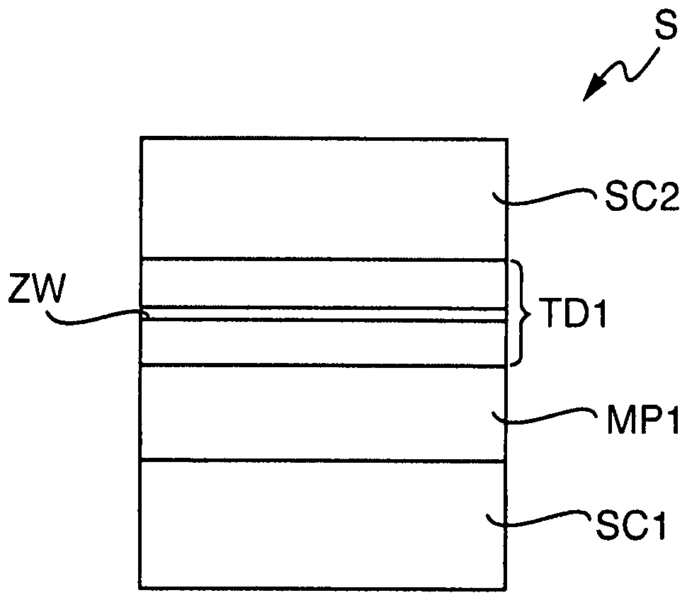
Die Abbildung der
Die erste Teilzelle SC1 weist eine erste Bandlücke
Die zweite Teilzelle weist eine zweite Bandlücke
Der metamorphe Puffer MP1 gleicht die Unterschiede zwischen den Gitterkonstanten
Die Tunneldiode
Die n+-Schicht der ersten Tunneldiode
Die Zwischenschicht
In der Abbildung der
Die Mehrfachsolarzelle
In der Abbildung der
In dieser Ausführungsform umfasst die Mehrfachsolarzelle
Während eine zweite Tunneldiode
Die dritte Tunneldiode
Die erste Teilzelle
In der Abbildung der
Die Mehrfachsolarzelle ist als 5-fach Zelle ausgebildet. Auf der als Ge-Substrat ausgebildeten ersten Teilzelle
Auf der zweiten Tunneldiode
Die erste Tunneldiode umfasst eine AlInGaAs-Schicht als p+-Schicht, eine InGaP-Schicht als n+-Schicht und zwischen der n+-Schicht und der p+-Schicht eine Zwischenschicht
Die zweite Tunneldiode
Die dritte und die vierte Tunneldiode
Alternativ umfasst auch die vierte Tunneldiode
Es versteht sich, dass die erfindungsgemäße Tunneldiode ohne weiteres auch in gitterangepasste Mehrfachsolarzellen, d.h. Solarzellenstapel ohne einen metamorphen Puffer einbauen lässt. Hierbei lässt sich die erste Zelle auch aus einem anderen Material als Germanium z.B. aus GaAs ausbilden.It goes without saying that the tunnel diode according to the invention can also readily be used in grid-adapted multiple solar cells, i.e. Solar cell stack can be installed without a metamorphic buffer. The first cell can also be made of a material other than germanium e.g. train from GaAs.
Es sei des Weiteren angemerkt, dass die stapelförmige Solarzelle auch als intervertiert gewachsene Mehrfachsolarzelle mit und ohne metamorphen Puffer ausbilden lässt. Hierbei lassen sich alle Varianten auch monolithisch ausbilden. In einer anderen Weiterbildung umfasst die Mehrfachsolarzelle einen oder mehrere Waferbond und / oder einen metamorphen Puffer.It should also be noted that the stacked solar cell can also be designed as an interverted grown multiple solar cell with and without a metamorphic buffer. All variants can also be designed monolithically. In another development, the multiple solar cell comprises one or more wafer bonds and / or a metamorphic buffer.
ZITATE ENTHALTEN IN DER BESCHREIBUNG QUOTES INCLUDE IN THE DESCRIPTION
Diese Liste der vom Anmelder aufgeführten Dokumente wurde automatisiert erzeugt und ist ausschließlich zur besseren Information des Lesers aufgenommen. Die Liste ist nicht Bestandteil der deutschen Patent- bzw. Gebrauchsmusteranmeldung. Das DPMA übernimmt keinerlei Haftung für etwaige Fehler oder Auslassungen.This list of documents listed by the applicant has been generated automatically and is only included for the better information of the reader. The list is not part of the German patent or utility model application. The DPMA assumes no liability for any errors or omissions.
Zitierte PatentliteraturPatent literature cited
- EP 2251912 A1 [0003]EP 2251912 A1 [0003]
Zitierte Nicht-PatentliteraturNon-patent literature cited
- W. Guter et al, „Investigation and development of III-V-triple-junction concentrator solar cells“, in 22nd European Photovoltaic Solar Energy Conference, 3-7 September 2007, Milan Italy, S.122-125 [0002]W. Guter et al, "Investigation and development of III-V-triple-junction concentrator solar cells", in 22nd European Photovoltaic Solar Energy Conference, September 3-7, 2007, Milan Italy, p.122-125 [0002]
Claims (21)
Priority Applications (1)
| Application Number | Priority Date | Filing Date | Title |
|---|---|---|---|
| DE102018009850.9A DE102018009850B4 (en) | 2018-12-19 | 2018-12-19 | Stacked multi-junction solar cell |
Applications Claiming Priority (1)
| Application Number | Priority Date | Filing Date | Title |
|---|---|---|---|
| DE102018009850.9A DE102018009850B4 (en) | 2018-12-19 | 2018-12-19 | Stacked multi-junction solar cell |
Publications (2)
| Publication Number | Publication Date |
|---|---|
| DE102018009850A1 true DE102018009850A1 (en) | 2020-06-25 |
| DE102018009850B4 DE102018009850B4 (en) | 2025-08-21 |
Family
ID=70969048
Family Applications (1)
| Application Number | Title | Priority Date | Filing Date |
|---|---|---|---|
| DE102018009850.9A Active DE102018009850B4 (en) | 2018-12-19 | 2018-12-19 | Stacked multi-junction solar cell |
Country Status (1)
| Country | Link |
|---|---|
| DE (1) | DE102018009850B4 (en) |
Citations (5)
| Publication number | Priority date | Publication date | Assignee | Title |
|---|---|---|---|---|
| EP1134813A2 (en) * | 2000-03-15 | 2001-09-19 | The Boeing Company | Multijunction photovoltaic cell with thin first (top) subcell and thick second subcell of same or similar semiconductor material |
| EP2251912A1 (en) | 2009-05-11 | 2010-11-17 | Fraunhofer-Gesellschaft zur Förderung der angewandten Forschung e.V. | Tunnel diodes from strain-compensated compound semiconductor layers |
| US20100319764A1 (en) * | 2009-06-23 | 2010-12-23 | Solar Junction Corp. | Functional Integration Of Dilute Nitrides Into High Efficiency III-V Solar Cells |
| US20120227797A1 (en) * | 2007-09-24 | 2012-09-13 | Emcore Solar Power, Inc. | Heterojunction subcells in inverted metamorphic multijunction solar cells |
| US20170222066A1 (en) * | 2016-01-28 | 2017-08-03 | Solaero Technologies Corp. | Multijunction metamorphic solar cell for space applications |
Family Cites Families (2)
| Publication number | Priority date | Publication date | Assignee | Title |
|---|---|---|---|---|
| GB0917747D0 (en) | 2009-10-09 | 2009-11-25 | Univ Glasgow | Intermediate band semiconductor photovoltaic devices, uses thereof and methods for their manufacture |
| JP6582591B2 (en) | 2014-07-11 | 2019-10-02 | 株式会社リコー | Compound semiconductor solar cell and method of manufacturing compound semiconductor solar cell |
-
2018
- 2018-12-19 DE DE102018009850.9A patent/DE102018009850B4/en active Active
Patent Citations (5)
| Publication number | Priority date | Publication date | Assignee | Title |
|---|---|---|---|---|
| EP1134813A2 (en) * | 2000-03-15 | 2001-09-19 | The Boeing Company | Multijunction photovoltaic cell with thin first (top) subcell and thick second subcell of same or similar semiconductor material |
| US20120227797A1 (en) * | 2007-09-24 | 2012-09-13 | Emcore Solar Power, Inc. | Heterojunction subcells in inverted metamorphic multijunction solar cells |
| EP2251912A1 (en) | 2009-05-11 | 2010-11-17 | Fraunhofer-Gesellschaft zur Förderung der angewandten Forschung e.V. | Tunnel diodes from strain-compensated compound semiconductor layers |
| US20100319764A1 (en) * | 2009-06-23 | 2010-12-23 | Solar Junction Corp. | Functional Integration Of Dilute Nitrides Into High Efficiency III-V Solar Cells |
| US20170222066A1 (en) * | 2016-01-28 | 2017-08-03 | Solaero Technologies Corp. | Multijunction metamorphic solar cell for space applications |
Non-Patent Citations (2)
| Title |
|---|
| KANG, S. [u.a.]: Numerical analysis of p-GaAs/n-GaAs tunnel junction employing InAs intermediate layer for high concentrated photovoltaic applications. In: Journal of Physics: Conference Series, 490, 2014, 012178. - ISSN 1742-6596 (print) * |
| W. Guter et al, „Investigation and development of III-V-triple-junction concentrator solar cells", in 22nd European Photovoltaic Solar Energy Conference, 3-7 September 2007, Milan Italy, S.122-125 |
Also Published As
| Publication number | Publication date |
|---|---|
| DE102018009850B4 (en) | 2025-08-21 |
Similar Documents
| Publication | Publication Date | Title |
|---|---|---|
| EP2919276B1 (en) | Multijunction solar cell | |
| DE102005048102B4 (en) | Interdigital rectifier with multi-channel group III nitrite heterostructure | |
| DE102015016047A1 (en) | Multiple solar cell | |
| EP3419060B1 (en) | Solar cell stack | |
| DE102015016822B4 (en) | Stacked multi-junction solar cell | |
| EP2960950A1 (en) | Multiple solar cell | |
| DE102016015056A1 (en) | Production method of a layer stack of a p + -substrate, a p-layer, an n-layer and a third layer | |
| DE102019000588A1 (en) | Stack-shaped multiple solar cell | |
| DE102018009744A1 (en) | Stacked monolithic upright metamorphic multiple solar cell | |
| EP3012874B1 (en) | Integrated stacked multiple solar cell | |
| DE102018203509B4 (en) | quadruple solar cell for space applications | |
| DE102015006379A1 (en) | Scalable voltage source | |
| DE102015002513A1 (en) | solar cell device | |
| DE102010010880A1 (en) | Multijunction solar cell useful in satellite and other space related applications, comprises substrate, solar cells, germanium silicon tin buffer layer, germanium silicon tin back surface field layer, and germanium silicon tin window layer | |
| DE102018009850A1 (en) | Stack-shaped multiple solar cell | |
| DE102015013514A1 (en) | Optical receiver module | |
| EP3965168B1 (en) | Stacked monolithic multi-junction solar cell | |
| DE102019003068A1 (en) | InGaAS stacked high-blocking semiconductor power diode | |
| EP2947703B1 (en) | Solar cell stack | |
| DE102016208113A1 (en) | Multiple solar cell and its use | |
| DE102019002034A1 (en) | Stacked, monolithic, upright metamorphic, terrestrial concentrator solar cell | |
| DE102020001185A1 (en) | Stacked monolithic upright metamorphic III-V multi-junction solar cell | |
| EP3937259A1 (en) | Monolithic metamorphic multisolar cell | |
| DE102016005640A1 (en) | Inverted multiple solar cell | |
| DE102020004170A1 (en) | Stacked monolithic multi-junction solar cell |
Legal Events
| Date | Code | Title | Description |
|---|---|---|---|
| R012 | Request for examination validly filed | ||
| R079 | Amendment of ipc main class |
Free format text: PREVIOUS MAIN CLASS: H01L0031073500 Ipc: H01L0031072500 |
|
| R016 | Response to examination communication | ||
| R016 | Response to examination communication | ||
| R079 | Amendment of ipc main class |
Free format text: PREVIOUS MAIN CLASS: H01L0031072500 Ipc: H10F0010161000 |
|
| R018 | Grant decision by examination section/examining division |