DE102016118932B3 - DC buck converter - Google Patents
DC buck converter Download PDFInfo
- Publication number
- DE102016118932B3 DE102016118932B3 DE102016118932.4A DE102016118932A DE102016118932B3 DE 102016118932 B3 DE102016118932 B3 DE 102016118932B3 DE 102016118932 A DE102016118932 A DE 102016118932A DE 102016118932 B3 DE102016118932 B3 DE 102016118932B3
- Authority
- DE
- Germany
- Prior art keywords
- voltage
- signal
- output
- time
- constant
- Prior art date
- Legal status (The legal status is an assumption and is not a legal conclusion. Google has not performed a legal analysis and makes no representation as to the accuracy of the status listed.)
- Active
Links
Images
Classifications
-
- H—ELECTRICITY
- H02—GENERATION; CONVERSION OR DISTRIBUTION OF ELECTRIC POWER
- H02M—APPARATUS FOR CONVERSION BETWEEN AC AND AC, BETWEEN AC AND DC, OR BETWEEN DC AND DC, AND FOR USE WITH MAINS OR SIMILAR POWER SUPPLY SYSTEMS; CONVERSION OF DC OR AC INPUT POWER INTO SURGE OUTPUT POWER; CONTROL OR REGULATION THEREOF
- H02M3/00—Conversion of dc power input into dc power output
- H02M3/02—Conversion of dc power input into dc power output without intermediate conversion into ac
- H02M3/04—Conversion of dc power input into dc power output without intermediate conversion into ac by static converters
- H02M3/10—Conversion of dc power input into dc power output without intermediate conversion into ac by static converters using discharge tubes with control electrode or semiconductor devices with control electrode
- H02M3/145—Conversion of dc power input into dc power output without intermediate conversion into ac by static converters using discharge tubes with control electrode or semiconductor devices with control electrode using devices of a triode or transistor type requiring continuous application of a control signal
- H02M3/155—Conversion of dc power input into dc power output without intermediate conversion into ac by static converters using discharge tubes with control electrode or semiconductor devices with control electrode using devices of a triode or transistor type requiring continuous application of a control signal using semiconductor devices only
- H02M3/156—Conversion of dc power input into dc power output without intermediate conversion into ac by static converters using discharge tubes with control electrode or semiconductor devices with control electrode using devices of a triode or transistor type requiring continuous application of a control signal using semiconductor devices only with automatic control of output voltage or current, e.g. switching regulators
-
- H—ELECTRICITY
- H02—GENERATION; CONVERSION OR DISTRIBUTION OF ELECTRIC POWER
- H02M—APPARATUS FOR CONVERSION BETWEEN AC AND AC, BETWEEN AC AND DC, OR BETWEEN DC AND DC, AND FOR USE WITH MAINS OR SIMILAR POWER SUPPLY SYSTEMS; CONVERSION OF DC OR AC INPUT POWER INTO SURGE OUTPUT POWER; CONTROL OR REGULATION THEREOF
- H02M1/00—Details of apparatus for conversion
- H02M1/14—Arrangements for reducing ripples from dc input or output
- H02M1/15—Arrangements for reducing ripples from dc input or output using active elements
-
- H—ELECTRICITY
- H02—GENERATION; CONVERSION OR DISTRIBUTION OF ELECTRIC POWER
- H02M—APPARATUS FOR CONVERSION BETWEEN AC AND AC, BETWEEN AC AND DC, OR BETWEEN DC AND DC, AND FOR USE WITH MAINS OR SIMILAR POWER SUPPLY SYSTEMS; CONVERSION OF DC OR AC INPUT POWER INTO SURGE OUTPUT POWER; CONTROL OR REGULATION THEREOF
- H02M1/00—Details of apparatus for conversion
- H02M1/0003—Details of control, feedback or regulation circuits
- H02M1/0025—Arrangements for modifying reference values, feedback values or error values in the control loop of a converter
Abstract
Die Erfindung betrifft ein Verfahren zur Gleichspannungswandlerregelung mit einem Spannungseingang (Vin) und einem Spannungsausgang (Vout) nach einem Konstant-Ein- oder Konstant-Aus-Zeit-Verfahren, der zur Wandlung der Spannung mindestens einen Schalter (S1) aufweist und wobei die Zeitpunkte des periodischen Öffnens und Schließens des Schalters (S1) mittels eines Schaltsignal (SS1). von dem Potenzialverlauf an seinem Spannungsausgang (Vout) abhängen. Die Dauer (TE) der Ein-Zeit (TE) ist im Falle eines Konstant-Ein-Zeit-Verfahrens konstant bzw. die Dauer (TA) der Aus-Zeit (TA) im Falle eines Konstant-Aus-Zeit-Verfahrens. Das Potenzial eines internen Spannungssignals (Vi), dessen Potenzial von der Ausgangsspannung am Spannungsausgang (Vout) abhängt, wird durch einen Komparator (COMP) erfasst und mit einer Referenzspannung (Ref) verglichen. Dieser erzeugt ein Komparatorausgangssignal (Cs). Die Zeit, in der das Komparatorausgangssignal (Cs) sich im Zustand („AN“) befindet wird auf eine Mindestzeit zur Erzeugung des Schaltsignals (SS1) im Falle eines Konstant-Ein-Zeit-Verfahrens verlängert. Die Zeit, in der das Komparatorausgangssignal (Cs) sich im Zustand („AUS“) befindet wird auf eine Mindestzeit zur Erzeugung des Schaltsignals (SS1) im Falle eines Konstant-Aus-Zeit-Verfahrens verlängert. Eine Offsetspannung (Voff) wird in Abhängigkeit von dem Schaltsignal (SS1) zwischen dem Potenzial am Spannungsausgang (Vout) und dem internen Spannungssignal (Vi) zur Erzeugung dieses internen Spannungssignals (Vi) erzeugt.The invention relates to a method for DC-DC converter control with a voltage input (Vin) and a voltage output (Vout) according to a constant-on or constant-off-time method, which has at least one switch (S1) for converting the voltage and wherein the times the periodic opening and closing of the switch (S1) by means of a switching signal (SS1). depend on the potential profile at its voltage output (Vout). The duration (TE) of the on-time (TE) is constant in the case of a constant-on-time method or the duration (TA) of the off-time (TA) in the case of a constant-off-time method. The potential of an internal voltage signal (Vi) whose potential depends on the output voltage at the voltage output (Vout) is detected by a comparator (COMP) and compared with a reference voltage (Ref). This generates a comparator output signal (Cs). The time in which the comparator output signal (Cs) is in the state ("ON") is extended to a minimum time for generating the switching signal (SS1) in the case of a constant on-time method. The time in which the comparator output signal (Cs) is in the state ("OFF") is extended to a minimum time for generating the switching signal (SS1) in the case of a constant-off-time method. An offset voltage (Voff) is generated in response to the switching signal (SS1) between the potential at the voltage output (Vout) and the internal voltage signal (Vi) to produce this internal voltage signal (Vi).
Description
Einleitung introduction
Die Erfindung betrifft einen Gleichspannungsabwärtswandler und ist auch für andere Architekturen verwendbar, bei denen die Einschaltdauer oder Ausschaltdauer eines Schalters konstant ist und die jeweils andere Größe in Abhängigkeit von dem Potenzial an einem Spannungsausgang geregelt wird. Bei der Erfindung handelt es sich von der Grundkonstruktion her um einen Gleichspannungswandler, der einen Constant-On-Time Regler umfasst. Die Aus-Zeit wird bei diesem Spannungsreglertyp angepasst und durch eine Regelschleife in der Art nachgeregelt, sodass sich die gewünschte Ausgangsspannung am Spannungsausgang (Vout) des Gleichspannungswandlers einstellt. Die Ein-Zeit zu der der Schalter (S1) eingeschaltet ist, also geschlossen ist, ist dabei konstant. Daher der englische Name Konstant-Ein-Zeit-Regler. Selbstverständlich kann dieses Prinzip aus dem Stand der Technik auch für Spannungsregler mit einer konstanten Aus-Zeit und einer geregelten Ein-Zeit verwendet werden. Die entsprechende Bezeichnung ist Konstant-Aus-Zeit-Regler. Die folgende Beschreibung der Erfindung beschreibt zur Vereinfachung der Beschreibung zwar einen DC-DC Spannungsregler mit einer Grundstruktur, die einen Spannungsregler mit konstanter Ein-Zeit umfasst, die Erfindung bezieht sich jedoch auf beider Arten von Spannungsreglern. Spannungsregler mit konstanter Aus-Zeit sind also von der Erfindung ebenfalls umfasst. Solche Spannungsregler werden auch als Puls-Frequenz-Regler oder Puls-Frequenzwandler oder PFM-Regler bezeichnet. The invention relates to a DC buck converter and is also applicable to other architectures in which the ON time or OFF duration of a switch is constant and the other variable is regulated as a function of the potential at a voltage output. In the invention, the basic construction is a DC-DC converter comprising a constant-on-time regulator. The off-time is adjusted in this type of voltage regulator and readjusted by a control loop in the way, so that the desired output voltage at the voltage output (V out ) sets the DC-DC converter. The on-time to which the switch (S 1 ) is turned on, that is closed, is constant. Hence the English name Constant-On-Time-Regulator. Of course, this principle of the prior art can also be used for voltage regulators with a constant off-time and a controlled on-time. The corresponding designation is Constant-Off-Time-Regulator. Although the following description of the invention describes a DC-DC voltage regulator having a basic structure including a constant on-time voltage regulator for convenience of description, the invention relates to both types of voltage regulators. Voltage regulators with constant off-time are therefore also included in the invention. Such voltage regulators are also referred to as pulse-frequency controllers or pulse-frequency converters or PFM controllers.
Ein solcher Spannungsregler aus dem Stand der Technik ist in
Die einfachste Methode besteht somit zwar aus einer Messung der Ausgangsspannung als Stellgröße des Spannungsreglers und einer Nachregelung der Aus-Zeit (Konstant-Ein-Zeit-Regler), ein Problem ist jedoch der Widerstand (RESR) (ESR = equivalent series resistance = äquivalenter Serienwiderstand) vor der Speicherkapazität (C1) Kondensator, weil das System sonst keine Information über den elektrischen Spulenstrom (IL) durch die Drosselspule (L1) hat. Die Funktion des ESR-Widerstands (RESR) ist es, das Regelverhalten zu optimieren. Although the simplest method thus consists of a measurement of the output voltage as the manipulated variable of the voltage regulator and a readjustment of the off-time (constant on-time regulator), a problem is the resistance (R ESR ) (ESR = equivalent series resistance = equivalent Series resistor) before the storage capacitor (C 1 ) capacitor, because otherwise the system has no information about the electrical coil current (I L ) through the choke coil (L 1 ). The function of the ESR resistor (R ESR ) is to optimize the control behavior.
Diese Verwendung des Widerstands (RESR), wie im Stand der Technik üblich, hat zwei Nachteile:
- 1. Auf der Ausgangsspannung am Spannungsausgang (Vout) entsteht ein dem konstanten Spannungspegel überlagertes periodisches Dreieckssignal, das durch den über den Widerstand (RESR) abfallenden Lade- und Entladestrom der Speicherkapazität (C1) hervorgerufen wird. Dieses Dreieckssignal entsteht aufgrund der durch die Drosselspule erzwungenen Stromkonstanz und der Integration durch die Speicherkapazität (C1). Bei einer Zustandsänderung des Schaltsignals (SS1) von „AN“ nach „AUS“ und umgekehrt wechselt auch die Steigung dieses überlagerten Dreieckssignals.
- 2. Der Widerstand (RESR) ist zunächst der parasitische Zuleitungswiderstand der Speicherkapazität (C1), der relativ undefiniert ist. Daher wird oft ein überdimensionierter zusätzlicher ESR-Widerstand (RESR) in Serie zum Kondensator eingebaut. Um den Ausgangswiderstand des Systems gering zu halten, werden kleine Widerstandswerte bevorzugt. Ein 20mOhm Widerstand (RESR) ist aber erfahrungsgemäß relativ teuer.
- 1. On the output voltage at the voltage output (V out ) results in a constant voltage level superimposed periodic triangular signal, which is caused by the across the resistor (R ESR ) falling charge and discharge current of the storage capacity (C 1 ). This triangular signal is due to the forced by the choke coil current constancy and integration by the storage capacity (C 1 ). When the switching signal (SS 1 ) changes from "ON" to "OFF" and vice versa, the slope of this superimposed triangular signal also changes.
- 2. The resistance (R ESR ) is initially the parasitic lead resistance of the storage capacitance (C 1 ), which is relatively undefined. Therefore, an oversized additional ESR resistor (R ESR ) is often installed in series with the capacitor. To keep the output resistance of the system low, small values of resistance are preferred. However, experience has shown that a 20mOhm resistor (R ESR ) is relatively expensive.
Aus der
Die technische Lehre der
Aus der IEEE Veröffentlichung von C. C. CHUANG et. al. „A Buck Converter Using Accurate Synthetic Ripple Hysteresis Control Scheme“ IEEE PEDS 2011, Singapore, 5–8-December 2011 (im Folgenden nur kurz IEEE Veröffentlichung genannt) ist ebenfalls ein Gleichspannungswandler mit Current-Mode-Regelung bekannt. In deren
Auch in der Zusammenschau lösen sowohl die IEEE Veröffentlichung als auch die
Aufgabe der Erfindung Object of the invention
Ziel ist es, den Ausgangsripple und den zusätzlichen ESR-Widerstand (RESR) ohne die Nachteile aus dem Stand der Technik (z.B. die fünf Nachteile der
Diese Aufgabe wird durch ein Verfahren nach Anspruch 1 gelöst. This object is achieved by a method according to
Beschreibung der Erfindung Description of the invention
Ein grundlegender Gedanke der Erfindung ist es, ähnlich wie in der
Aus der
Bei der Erfindung handelt es sich um ein Verfahren und eine entsprechende Vorrichtung zur Regelung eines Gleichspannungswandlers nach einem Konstant-Ein-Zeit-Verfahren oder alternativ nach einem Konstant-Aus-Zeit-Verfahren. Das Verfahren umfasst mehrere Schritte, die typischerweise zeitlich parallel oder quasiparallel in beliebiger Reihenfolge und schneller Abfolge zyklisch ausgeführt werden. Die erfindungsgemäße Vorrichtung umfasst als ersten Schritt das periodisch wiederkehrende Schließen und Öffnen eines ersten Schalters (S1) zwischen einem Spannungseingang (Vin) und einem Zwischenknoten (Z1). Dieses Öffnen und Schließen des ersten Schalters (S1) wird dabei mittels eines vorzugsweise wertdiskreten, zeitkontinuierlichen oder zeitdiskreten Schaltsignals (SS1) mit einer Schaltperiode (TP) gesteuert. Die Schaltperiode (TP) ist dabei in eine Ein-Zeit (TE), in der das Schaltsignal (SS1) an ist und der erste Schalter (S1) geschlossen ist, und eine nachfolgende Aus-Zeit (TA), in der das Schaltsignal (SS1) aus ist und der erste Schalter (S1) offen ist, aufgeteilt. Die Dauer (TE) der Ein-Zeit (TE) ist im Falle eines Konstant-Ein-Zeit-Reglers dabei konstant. Demgegenüber ist stattdessen die Dauer (TA) der Aus-Zeit (TA) ist im Falle eines Konstant-Aus-Zeit-Reglers konstant. The invention relates to a method and a corresponding device for controlling a DC-DC converter according to a constant-on-time method or alternatively according to a constant-off-time method. The method comprises a plurality of steps, which are typically carried out in a time-parallel or quasi-parallel manner in any order and fast sequence cyclically. As a first step, the device according to the invention comprises the periodically recurring closing and opening of a first switch (S 1 ) between a voltage input (V in ) and an intermediate node (Z 1 ). This opening and closing of the first switch (S 1 ) is controlled by means of a preferably discrete-value, time-continuous or time-discrete switching signal (SS 1 ) with a switching period (T P ). The switching period (TP) is in a on-time (T E ), in which the switching signal (SS 1 ) is on and the first switch (S 1 ) is closed, and a subsequent off-time (T A ), in the switch signal (SS 1 ) is off and the first switch (S 1 ) is open, split. The duration (T E ) of the on-time (T E ) is constant in the case of a constant on-time controller. In contrast, instead, the duration (T A ) of the off-time (T A ) is constant in the case of a constant-off-time regulator.
Als zweiten Schritt umfasst das erfindungsgemäße Verfahren die Glättung des Ausgangsstromes (Iout), der aus dem Spannungsausgang (Vout) heraus fließt, mittels einer Drosselspule (L1) zwischen dem Zwischenknoten (Z1) und dem Spannungsausgang (Vout). Ein weiterer Schritt betrifft das Speichern und/oder die Abgabe einer Ladungsmenge aus dem Spannungsausgang (Vout) in eine Speicherkapazität (C1) hinein bzw. aus dieser heraus. Aus dem elektrischen Potenzial wird ein internes Spannungssignal (Vi) erzeugt, dessen Spannung oder zumindest dessen Wert von dem potenzial am Spannungsausgang (Vout) abhängt. Dies geschieht erfindungsgemäß durch einen kapazitiv/ohmschen Spannungsteiler (Ci1, Ci2, R1, R2) aus einem ersten Kondensator (Ci1), einem zweiten Kondensator (Ci2), einem ersten Spannungsteilerwiderstand (R1) und einem zweiten Spannungsteilerwiderstand (R2). Die Verwendung von Spannungsteilerwiderständen (R1, R2) ist zwar aus der
Nun wird in dem erfindungsgemäßen Verfahren durch eine zusätzliche Vorrichtung (I1, Is) das oben erwähnte Dreieckssignal als Spannungsdreieckssignal bzw. Wertdreieckssignal auf das interne Spannungssignal (Vi) aufaddiert, das die Wirkung des Widerstandes (RESR) emuliert. Dadurch wird die Erzeugung dieses überlagernden Dreieckssignals auf der Ausgangsspannung des Spannungsausgangs (Vout) wie bei der
Im Gegensatz zum Stand der Technik und zwar insbesondere auch im Gegensatz zur
In einer anderen Ausprägung der Erfindung umfasst das Verfahren die Erzeugung eines Ausgangsstromes (IBuf) einer Pufferschaltung (Buf) zur Erzeugung des internen Spannungssignals (Vi). Dieses ist wie zuvor wieder proportional zu der Spannung am Spannungsausgang (Vout). Die Erzeugung des Ausgangsstromes (IBuf) erfolgt dabei vorzugsweise durch diese Pufferschaltung (Buf), die einen Ausgangswiderstand (Ra) besitzt. Hierdurch fließt ein Ausgangsstrom (IBuf) aus der Pufferschaltung (Buf) in den Konten des internen Spannungssignals (Vi), der von diesem Ausgangswiderstand (Ra) der Pufferschaltung (Buf) und der Spannungsdifferenz zwischen dem Potenzial am Ausgang der Pufferschaltung (Buf) und dem Potenzial des internen Spannungssignals (Vi) bestimmt wird. Mit diesem Ausgangsstrom (IBuf) der Pufferschaltung (Buf) wird ein Kondensator (Ci) geladen bzw. entladen. Damit folgt die Spannung über diesen Kondensator (Ci) tiefpassgefiltert und multipliziert mit einem durch die Pufferschaltung (Buf) vorgebbaren Faktor der Ausgangsspannung am Spannungsausgang (Vout). Um nun das überlagerte Dreieckssignal auf dem Potenzial des Spannungsausgangs (Vout) zu emulieren, wird in dieser Variante der Erfindung der Kondensator (Ci) mittels des Ausgangsstromes einer steuerbaren bipolaren Konstantstromquelle (Is) kurzzeitig geladen bzw. entladen. Deren Polarität hängt dabei in diesem Beispiel von dem Schaltsignal (SS1) ab. Um einen kontinuierlichen Anstieg oder einen kontinuierlichen Abfall des Potenzials des internen Spannungssignals zu vermeiden und die Signalqualität des Ausgangssignals zu erhalten, die für die typische Verwendung in Kraftfahrzeugen sinnvoll ist, muss der zeitliche Mittelwert der Stromsumme der in den Knoten des internen Spannungssignals (Vi) hineinfließenden Ströme und der aus diesem Knoten herausfließenden Ströme bei Mittelwertbildung im eingeschwungenen Zustand zu einer Spannungsänderung am Kondensator (Ci) führen, die nicht mehr als 200µV betragen darf. Natürlich können bei entsprechender Qualitätsminderung auch größere Werte wie beispielsweise 400µV, 800µV oder gar 1,6V zugelassen werden. Umgekehrt kann die Qualität gesteigert werden, wenn die Schaltung so ausgelegt wird, dass die Schwankungen kleiner als 100µV oder gar kleiner als 50µV gehalten werden. In another embodiment of the invention, the method comprises generating an output current (I Buf ) of a buffer circuit (Buf) for generating the internal voltage signal (V i ). As before, this is again proportional to the voltage at the voltage output (V out ). The generation of the output current (I Buf ) is preferably carried out by this buffer circuit (Buf), which has an output resistance (R a ). Thereby flows an output current (I Buf ) from the buffer circuit (Buf) in the accounts of the internal voltage signal (V i ), of this output resistance (R a ) of the buffer circuit (Buf) and the voltage difference between the potential at the output of the buffer circuit (Buf ) and the potential of the internal voltage signal (V i ). This output current (I Buf) of the buffer circuit (BUF) is loaded, a capacitor (C i) or discharged. Thus, the voltage across this capacitor (C i ) low-pass filtered and multiplied by a predetermined by the buffer circuit (Buf) factor of the output voltage at the voltage output (V out ). In order to emulate the superimposed triangular signal at the potential of the voltage output (V out ), the capacitor (C i ) is briefly charged or discharged in this variant of the invention by means of the output current of a controllable bipolar constant current source (I s ). Their polarity depends in this example on the switching signal (SS 1 ). In order to avoid a continuous increase or decrease of the potential of the internal voltage signal and to obtain the signal quality of the output signal, which is useful for the typical use in motor vehicles, the time average of the current sum in the nodes of the internal voltage signal (V i ) flowing in currents and the outflowing from this node currents in averaging in the steady state to a voltage change across the capacitor (C i ) lead, which may not be more than 200μV. Of course, with a corresponding reduction in quality, larger values such as 400μV, 800μV or even 1.6V can be allowed. Conversely, the quality can be increased if the circuit is designed so that the variations are kept smaller than 100μV or even smaller than 50μV.
Auch in einer weiteren Ausprägung der Erfindung wird das Potenzial des internen Spannungssignals (Vi), dessen Potenzial auch hier von der Ausgangsspannung am Spannungsausgang (Vout) abhängt, durch einen Komparator (COMP) mit einer Referenzspannung (Ref) verglichen. Der Komparator (COMP) erzeugt als Vergleichsergebnis das Komparatorausgangssignal (Cs), das je nach Vergleichsergebnis den Wert „An“ oder „Aus“ haben kann, also vorzugsweise ein wertdiskretes binäres Signal ist. Wie zuvor verlängert eine Pulsverlängerungseinheit (PV) die Zeit, in der das Komparatorausgangssignal (Cs) sich im Falle eines Konstant-Ein-Zeit-Reglers im Zustand „An“ bzw. im Falle eines Konstant-Aus-Zeit-Reglers im Zustand „Aus“ befindet, auf eine Mindestzeit und erzeugt daraus das Schaltsignal (SS1). In diesem Fall erzeugt eine Pufferschaltung (Buf) einen Ausgangsstrom (IBuf) in den Knoten des internen Spannungssignals (Vi) hinein, das damit erzeugt wird. Das interne Spannungssignal (Vi) ist bis auf das im Folgenden beschriebene überlagerte Dreieckssignal proportional zu dem Potenzial des Spannungsausgangs (Vout) gegenüber dem Bezugspotenzial. Dieser Basisverlauf des internen Spannungssignals (Vi) bildet einen ersten Spannungssignalanteil des internen Spannungssignals (Vi). Die Pufferschaltung (Buf) besitzt dabei einen Ausgangswiderstand (Ra), der von Null verschieden ist. Durch diesen Ausgangswiderstand (Ra) kann sich das interne Spannungssignal (Vi) auf einem anderen Potenzial als der Ausgang der Pufferschaltung (Buf) befinden. Dieser Ausgangsstrom (IBuf) der Pufferschaltung (Buf) wird nun in dieser Ausprägung der Erfindung zum Laden eines Kondensators (Ci) verwendet. Hierdurch stellt sich ein Potenzial des inneren Spannungssignals (Vi) ein, das zunächst im Wesentlichen dem Potenzial des Ausgangs der Pufferschaltung (Buf) als erster Spannungssignalanteil des internen Spannungssignals (Vi) entspricht. In a further embodiment of the invention, the potential of the internal voltage signal (V i ) whose potential depends here also on the output voltage at the voltage output (V out ) is compared by a comparator (COMP) with a reference voltage (Ref). The comparator (COMP) generates as a result of comparison the comparator output signal (C s ), which depending on the result of the comparison may have the value "on" or "off", that is to say preferably a discrete-value binary signal. As before, a pulse extension unit (PV) extends the time in which the comparator output signal (C s ) in the state "on" in the case of a constant on-time controller or in the state in the case of a constant-off-time controller. Off "is at a minimum time and generates the switching signal (SS 1 ). In this case, a buffer circuit (Buf) generates an output current (I Buf ) into the node of the internal voltage signal (V i ) generated therewith. The internal voltage signal (V i ) is proportional to the potential of the voltage output (V out ) with respect to the reference potential except for the superimposed triangular signal described below. This base curve of the internal voltage signal (V i ) forms a first voltage signal component of the internal voltage signal (V i ). The buffer circuit (Buf) has an output resistance (R a ) which is different from zero. Through this output resistance (R a ), the internal voltage signal (V i ) may be at a different potential than the output of the buffer circuit (Buf). This output current (I Buf ) of the buffer circuit (Buf) is now used in this embodiment of the invention for charging a capacitor (C i ). As a result, a potential of the internal voltage signal (V i ) sets, which first substantially corresponds to the potential of the output of the buffer circuit (Buf) as the first voltage signal component of the internal voltage signal (V i ).
Dieser erste Spannungssignalanteil (Vi) weist den besagten Basisverlauf auf. Typischerweise ist die Pufferschaltung (Buf) so gestaltet, dass das Potenzial seines idealen widerstandslosen Ausgangs der Pufferschaltung (Buf), also ohne Ausgangswiderstand (Ra), direkt proportional zum Potenzial des Spannungsausgangs (Vout) ist. Um nun das Dreieckssignal auf der Ausgangsspannung (Vout) zu emulieren, lädt und entlädt eine steuerbare Konstantstromquelle (Is) aus einer ersten Konstantstromquelle (Is1) und einer zweiten Konstantstromquelle (Is2) diesen Kondensator (Ci) zusätzlich mittels ihres Ausgangsstromes und erzeugt so eine zusätzliche fallende bzw. steigende Spannungsrampe auf dem internen Spannungssignal (Vi) als zweiten Spannungssignalanteil. Die steuerbare erste Konstantstromquelle (Is1) wird dabei abhängig vom Schaltsignal (SS1), das ja gleichzeitig auch den ersten Schalter (S1) steuert, ein und ausgeschaltet. In dieser Variante der Erfindung wird gleichzeitig der Kondensator (Ci) von der zweiten Konstantstromquelle (Is2) mittels ihres Ausgangsstromes geladen bzw. entladen, deren Polarität ebenfalls vom Schaltsignal (SS1) abhängt. Auch hier muss dafür Sorge getragen werden, dass der zeitliche Mittelwert der Stromsumme der in den Knoten des internen Spannungssignals (Vi) hineinfließenden Ströme und der aus diesem Knoten herausfließenden Ströme bei Mittelwertbildung im eingeschwungenen Zustand zu einer Spannungsänderung am Kondensator (Ci) führt, die wieder nicht mehr als 200µV beträgt. Das oben hinsichtlich dieses Limits gesagte trifft auch hier zu. This first voltage signal component (V i ) has the said base profile. Typically, the buffer circuit (BUF) is designed so that the potential of its ideal resistance-free output of the buffer circuit (BUF), which excludes output resistance (R a), directly proportional to the potential of the output voltage (V out). In order to emulate the triangular signal at the output voltage (V out ), a controllable constant current source (I s ) of a first constant current source (I s1 ) and a second constant current source (I s2 ) additionally charges and discharges this capacitor (C i ) by means of its output current and thus generates an additional falling or rising voltage ramp on the internal voltage signal (V i ) as the second voltage signal component. The controllable first constant current source (I s1 ) is switched on and off depending on the switching signal (SS 1 ), which also controls the first switch (S 1 ) at the same time. In this variant of the invention, the capacitor (C i ) is simultaneously charged or discharged by the second constant current source (I s2 ) by means of its output current, the polarity of which also depends on the switching signal (SS 1 ). Here, too, care must be taken that the mean value of the current sum of the currents flowing into the nodes of the internal voltage signal (V i ) and the currents flowing out of this node leads to a voltage change at the capacitor (C i ) when the steady-state averaging occurs, again not more than 200μV. The above with regard to this limit also applies here.
In einer daraus abgeleiteten Variante der Erfindung lädt der Ausgangsstrom der ersten steuerbaren Konstantstromquelle (Is1), die abhängig vom Schaltsignal (SS1) ein- und ausgeschaltet wird, den Kondensator (Ci). Der Ausgangsstrom der zweiten steuerbaren Konstantstromquelle (Is2), die nun abhängig vom Schaltsignal (SS1) nur dann eingeschaltet wird, wenn die erste Konstantstromquelle (Is1) ausgeschaltet ist, lädt den Kondensators (Ci) und erzeugt somit einen dritten Spannungssignalanteil. Dabei kann es beispielsweise auch vorkommen, dass beide Konstantstromquellen (IS1, IS2) zeitweise gleichzeitig ausgeschaltet sind. In a variant of the invention derived therefrom, the output current of the first controllable constant current source (I s1 ), which is switched on and off depending on the switching signal (SS 1 ), charges the capacitor (C i ). The output current of the second controllable constant current source (I s2 ), which is now switched on depending on the switching signal (SS 1 ) only when the first constant current source (I s1 ) is turned off, charges the capacitor (C i ) and thus generates a third voltage signal component. It may also happen, for example, that both constant current sources (IS 1 , IS 2 ) are temporarily switched off at the same time.
Alternativ kann in einer anderen Ausprägung der Erfindung vorgesehen sein, den Kondensator (Ci) mittels des Ausgangsstromes einer steuerbaren Konstantstromquelle (Is) zu laden oder zu entladen, deren Polarität vom Schaltsignal (SS1) abhängt. Alternatively, it may be provided in another embodiment of the invention to charge or discharge the capacitor (C i ) by means of the output current of a controllable constant current source (I s ) whose polarity depends on the switching signal (SS 1 ).
In einer anderen Ausprägung der Erfindung wird ein Messstrom, vorzugsweise als Ausgangsstrom (IBuff) der besagten Pufferschaltung (Buf), in Abhängigkeit von der Ausgangsspannung am Spannungsausgang (Vout) zur Erzeugung eines internen Spannungssignals (Vi) verwendet, der proportional zu der Spannung am Spannungsausgang (Vout) ist. Dabei durchfließt der Messstrom zumindest virtuell den Ausgangswiderstand (Ra). Der Messstrom (IBuf) wird also durch eine Teilvorrichtung, nämlich die Pufferschaltung (Buf), erzeugt, die einen Kleinsignalausgangswiderstand (Ra) besitzt. Mit diesem Messstrom, nämlich den Ausgangsstrom (IBuf) der Pufferschaltung (Buf), werden nun einer oder mehrere Kondensatoren (Ci1, Ci2) geladen bzw. entladen. Erfindungsgemäß werden zusätzlich diese Kondensatoren (Ci1, Ci2) mittels des Ausgangsstromes einer steuerbaren Konstantstromquelle (Is), deren Polarität vom Schaltsignal (SS1) abhängt, geladen bzw. entladen, um das Dreieckssignal auf dem Potenzialverlauf des Spannungsausgangs (Vout), wie er im Stand der Technik auftritt, vorzutäuschen. In another embodiment of the invention, a measuring current, preferably as output current (I buff ) of said buffer circuit (Buf), in dependence on the output voltage at the voltage output (V out ) is used to generate an internal voltage signal (V i ) proportional to the Voltage at the voltage output (V out ) is. The measuring current flows at least virtually through the output resistance (R a ). The measuring current (I Buf ) is thus generated by a sub-device, namely the buffer circuit (Buf), which has a small-signal output resistance (R a ). With this measurement current, namely the output current (I Buf ) of the buffer circuit (Buf), one or more capacitors (C i1 , C i2 ) are now charged or discharged. According to the invention, these capacitors (C i1 , C i2 ) are additionally charged or discharged by means of the output current of a controllable constant current source (I s ), the polarity of which depends on the switching signal (SS 1 ), in order to generate the triangular signal on the potential curve of the voltage output (V out ). , as it occurs in the prior art, pretend.
Neben den bisher beschriebenen Ausprägungen der Vorrichtung und des Verfahrens als Abwärtswandler kann die Erfindung auch als Aufwärtswandler ausgeführt werden. In addition to the previously described embodiments of the device and the method as a down converter, the invention can also be carried out as an up-converter.
Das erfindungsgemäße Verfahren zur Regelung eines Gleichspannungswandlers, der wieder einen Spannungseingang (Vin) und einen Spannungsausgang (Vout) besitzt, kann wieder wie zuvor nach einem Konstant-Ein-Zeit-Verfahren mit einer konstanten Ein-Zeit (TE) oder alternativ nach dem Konstant-Aus-Zeit-Verfahren mit einer konstanten Aus-Zeit (TA) durchgeführt werden. Die folgenden Schritte können parallel oder sequentiell, vorzugsweise schnell hintereinander in beliebiger Reihenfolge ausgeführt werden. Ein erster Schritt betrifft in diesem Fall die Glättung des Eingangsstromes (Iin), der in den Spannungseingang (Vin) hinein fließt, mittels einer Drosselspule (L1) zwischen einem Zwischenknoten (Z1) und dem Spannungseingang (Vin). Ein weiterer Schritt umfasst das periodische, wiederkehrende Schließen und Öffnen eines ersten Schalters (S1) zwischen diesem Zwischenknoten (Z1) und einem Bezugspotenzial mittels eines Schaltsignals (SS1). Das Schaltsignal (SS1) besitzt wieder einen ersten Zustand („AN“) und einen zweiten Zustand („AUS“) und eine Schaltperiode (TP). Die Schaltperiode (TP) ist wieder in eine Ein-Zeit (TE), in der das Schaltsignal (SS1) im ersten Zustand („AN“) ist und der Schalter (S1) geschlossen ist, und eine nachfolgende Aus-Zeit (TA), in der das Schaltsignal (SS1) im zweiten Zustand („AUS“) ist und der Schalter (S1) offen ist, aufgeteilt. Die Dauer (TE) der Ein-Zeit (TE) ist im Falle eines Konstant-Ein-Zeit-Verfahrens konstant. Die Dauer (TA) der Aus-Zeit (TA) ist im Falle eines Konstant-Aus-Zeit-Verfahrens konstant. Ein weiterer Schritt betrifft das Schließen eines zweiten Schalters (S2) zwischen dem Zwischenknoten (Z1) und dem Spannungsausgang (Vout), wenn die Potenzialdifferenz zwischen dem Spannungsausgang (Vout) und dem Zwischenknoten (Z1) abzüglich eines Spannungsoffsets ein erstes Vorzeichen hat und das Öffnen des zweiten Schalters (S2), wenn die Potenzialdifferenz zwischen dem Spannungsausgang (Vout) und dem Zwischenknoten (Z1) abzüglich des Spannungsoffsets ein zweites Vorzeichen hat, das dem ersten Vorzeichen entgegengesetzt ist. Dem Fachmann ist es dabei offensichtlich, dass es besonders bevorzugt ist, als zweiten Schalter (S2) eine Diode zu nutzen. Diese hat dabei typischerweise eine Schleusenspannung ab der die Diode öffnet und Strom durchlässt. Im Falle einer Diode als zweitem Schalter (S2) stellt diese Schleusenspannung den hier beschriebenen Spannungs-Offset dar. Schließlich umfasst das Verfahren das Speichern und/oder die Abgabe einer Ladungsmenge aus dem Spannungsausgang (Vout) in eine oder mehrere Speicherkapazitäten (C1) hinein oder aus diesen heraus. Das Erfassen des Potenzials eines internen Spannungssignals (Vi), dessen Potenzial von der Ausgangsspannung am Spannungsausgang (Vout) gegenüber einem Bezugspotenzial abhängt, gehört ebenfalls zu dem Verfahren. Typischerweise erfolgt die Erfassung durch einen Eingang eines Komparators (COMP). Dieser vergleicht das Potenzial an seinem Eingang mit einer Referenzspannung (Ref) und erzeugt eine Komparatorausgangssignal (Cs), das in Abhängigkeit vom Ergebnis des Vergleiches den einen ersten Zustand („AN“) oder einen zweiten Zustand („Aus“) haben kann. Im Falle eines Konstant-Ein-Zeit-Verfahrens umfasst ein weiterer Schritt das Verlängern einer Zeit, in der das Komparatorausgangssignal (Cs) sich im ersten Zustand („AN“) befindet auf eine Mindestzeit zur Erzeugung des Schaltsignals (SS1) durch eine Pulsverlängerungseinheit (PV). Alternativ dazu umfasst das Verfahren im Falle eines Konstant-Aus-Zeit-Verfahrens das Verlängern einer Zeit, in der das Komparatorausgangssignal (Cs) sich im zweiten Zustand („AUS“) befindet auf eine Mindestzeit zur Erzeugung des Schaltsignals (SS1) durch eine Pulsverlängerungseinheit (PV). The inventive method for controlling a DC-DC converter, which again has a voltage input (V in ) and a voltage output (V out ), can again as before according to a constant-on-time method with a constant on-time (T E ) or alternatively be performed according to the constant-off-time method with a constant off-time (T A ). The following steps can be performed in parallel or sequentially, preferably in quick succession in any order. A first step in this case relates to the smoothing of the input current (I in ), which flows into the voltage input (V in ), by means of a choke coil (L 1 ) between an intermediate node (Z 1 ) and the voltage input (Vin). A further step comprises the periodic, recurrent closing and opening of a first switch (S 1 ) between this intermediate node (Z 1 ) and a reference potential by means of a switching signal (SS 1 ). The switching signal (SS 1 ) again has a first state ("ON") and a second state ("OFF") and a switching period (T P ). The switching period (T P ) is again in an on-time (T E ), in which the switching signal (SS 1 ) in the first state ("ON") and the switch (S 1 ) is closed, and a subsequent output Time (T A ), in which the switching signal (SS 1 ) in the second state ("OFF") and the switch (S 1 ) is open, divided. The duration (T E ) of the on-time (T E ) is constant in the case of a constant-on-time method. The duration (T A ) of the off-time (T A ) is constant in the case of a constant-off-time method. A further step relates to the closing of a second switch (S 2 ) between the intermediate node (Z 1 ) and the voltage output (V out ) when the potential difference between the voltage output (V out ) and the intermediate node (Z 1 ) minus a voltage offset is a first And opening of the second switch (S 2 ) when the potential difference between the voltage output (V out ) and the intermediate node (Z 1 ) less the voltage offset has a second sign opposite to the first sign. It is obvious to a person skilled in the art that it is particularly preferable to use a diode as the second switch (S 2 ). This typically has a slip voltage from which the diode opens and lets current through. In the case of a diode as a second switch (S 2 ), this lock voltage represents the voltage offset described here. Finally, the method comprises the storage and / or the discharge of a charge amount from the voltage output (V out ) into one or more storage capacities (C 1 ) into or out of these. Detecting the potential of an internal voltage signal (V i ) whose potential depends on the output voltage at the voltage output (V out ) versus a reference potential also belongs to the method. Typically, the detection is performed by an input of a comparator (COMP). This compares the potential at its input with a reference voltage (Ref) and generates a comparator output signal (C s ) which, depending on the result of the comparison, may have a first state ("ON") or a second state ("OFF"). In the case of a constant-on-time method, a further step comprises extending a time in which the Comparator output signal (C s ) in the first state ("ON") is at a minimum time for generating the switching signal (SS 1 ) by a pulse extension unit (PV). Alternatively, in the case of a constant-off-time method, the method comprises extending a time in which the comparator output signal (C s ) is in the second state ("OFF") to a minimum time for generating the switching signal (SS 1 ) a pulse extension unit (PV).
In einer ersten Ausprägung als Aufwärtswandelverfahren zeichnet sich das Verfahren dadurch aus, dass es die periodische Erzeugung eines zeitlichen Überlagerungssignals, insbesondere eines Dreieckssignals, mit der zeitlichen Schaltperiode (Tp) im zeitlichen Potenzialverlauf des internen Spannungssignals (Vi) durch Addition eines zusätzlichen Überlagerungssignals, insbesondere eines Dreieckssignals, zeitsynchron zum Öffnen und/oder Schließen des ersten Schalters (S1) umfasst. In a first embodiment as Aufwärtswandelverfahren, the method is characterized in that it is the periodic generation of a temporal overlay signal, in particular a triangular signal, with the temporal switching period (T p ) in the temporal potential curve of the internal voltage signal (V i ) by adding an additional beat signal, in particular a triangular signal, time-synchronized to open and / or close the first switch (S 1 ).
Im Gegensatz zum Stand der Technik wird der Knoten dieses internen Spannungssignals (Vi), der an einen Kondensator (Ci) angeschlossen ist, zur Erzeugung des überlagernden Dreieckssignals nun jedoch zusätzlich durch eine steuerbare Konstantstromquelle (IS) mit einem zeitlich konstanten elektrischen Ladestrom der Konstantstromquelle (IS) geladen bzw. mit einem zeitlich konstanten elektrischen Entladestrom der Konstantstromquelle (IS) entladen, dessen Polarität vom Wert des Schaltsignals (SS1), das den ersten Schalter (S1) steuert, abhängt. Durch diese steuerbare Konstantstromquelle (Is) wird der Effekt des überlagerten Dreieckssignals auf dem zeitlichen Potenzialverlauf am Spannungsausgang (Vout) nun auf dem internen Spannungssignal (Vi) emuliert, sodass das interne Spannungssignal nun im Gegensatz zum Potenzialverlauf am Spannungsausgang (Vout) ein überlagertes Dreieckssignal zusätzlich aufweist. Da hier wieder eine sehr leicht realisierbare, sehr kompakte schaltbare Konstantstromquelle (Is) aus wenigen elektrischen Bauelementen in Kombination mit einer Ladekapazität, dem Kondensator (Ci), anstelle der Operationsverstärkerschaltung der
In einer zweiten Ausprägung als Aufwärtswandelverfahren zeichnet sich das Verfahren durch die periodische Erzeugung einer zeitlichen Überlagerungssignals, insbesondere eines Dreieckssignals, mit der zeitlichen Schaltperiode (Tp) im zeitlichen Wertverlauf des internen Spannungssignals (Vi) durch Addition eines geeigneten zusätzlichen Überlagerungssignals, insbesondere eines Dreieckssignals, zeitsynchron zum Öffnen und/oder Schließen des ersten Schalters (S1) aus. In a second embodiment as Aufwärtswandelverfahren, the method is characterized by the periodic generation of a temporal beat signal, in particular a triangular signal, with the temporal switching period (T p ) in the time course of the internal voltage signal (V i ) by adding a suitable additional beat signal, in particular a triangular signal , time-synchronized to open and / or close the first switch (S 1 ).
In einer dritten Ausprägung als Aufwärtswandelverfahren zeichnet sich das Verfahren durch die Erzeugung eines Ausgangsstromes (IBuf) einer Pufferschaltung (Buf) zur Erzeugung eines ersten Spannungssignalanteils des internen Spannungssignals (Vi) durch diese Pufferschaltung (Buf) aus, die einen Ausgangswiderstand (Ra) besitzt. Das Potenzial des internen Spannungssignals (Vi) ist dabei die Spannungssumme eines ersten Spannungssignalanteils und eines zweiten Spannungssignalanteils. Der erste Spannungsanteil ist dabei proportional zu der Spannung am Spannungsausgang (Vout). Das als Aufwärtswandelverfahren umfasst in dieser dritten Ausprägung das Laden eines oder mehrerer Kondensatoren (Ci1, Ci2) mit dem Ausgangsstrom (IBuf) der Pufferschaltung (Buf) zur Erzeugung des ersten Spannungssignalanteils sowie das Laden des oder der Kondensatoren (Ci1, Ci2) mittels des Ausgangsstromes einer steuerbaren Konstantstromquelle (Is), deren Polarität vom Schaltsignal (SS1) abhängt, zur Erzeugung des zweiten Spannungssignalanteils. In a third embodiment as an up- conversion method, the method is characterized by the generation of an output current (I Buf ) of a buffer circuit (Buf) for generating a first voltage signal component of the internal voltage signal (V i ) through this buffer circuit (Buf), which has an output resistance (R a ) owns. The potential of the internal voltage signal (V i ) is the voltage sum of a first voltage signal component and a second voltage signal component. The first voltage component is proportional to the voltage at the voltage output (V out ). The step-up method in this third embodiment comprises charging one or more capacitors (C i1 , C i2 ) with the output current (I Buf ) of the buffer circuit (Buf) for generating the first voltage signal component and charging the one or more capacitors (C i1 , C i2 ) by means of the output current of a controllable constant current source (Is), whose polarity depends on the switching signal (SS 1 ), for generating the second voltage signal component.
In einer vierten Ausprägung als Aufwärtswandelverfahren zeichnet sich das Verfahren durch die Erzeugung eines Ausgangsstromes (IBuf) einer Pufferschaltung (Buf) zur Erzeugung eines ersten Spannungssignalanteils des internen Spannungssignals (Vi) durch diese Pufferschaltung (Buf) aus, die einen Ausgangswiderstand (Ra) besitzt. Das Potenzial des internen Spannungssignals (Vi) ist dabei die Spannungssumme eines ersten Spannungssignalanteils und eines zweiten Spannungssignalanteils und eines dritten Spannungssignalanteils. Der erste Spannungssignalanteil ist dabei proportional zu der Spannung am Spannungsausgang (Vout). Das Aufwärtswandelverfahren umfasst in dieser vierten Ausprägung des Weiteren das Laden eines oder mehrerer Kondensatoren (Ci1, Ci2) mit dem Ausgangsstrom (IBuf) der Pufferschaltung (Buf) zur Erzeugung des ersten Spannungssignalanteils sowie das Laden des oder der Kondensatoren (Ci1, Ci2) mittels des Ausgangsstromes einer ersten steuerbaren Konstantstromquelle (Is1) zur Erzeugung des zweiten Spannungssignalanteils, die abhängig vom Schaltsignal (SS1) ein- und ausgeschaltet wird, und das Laden des oder der Kondensatoren (Ci1, Ci2) mittels des Ausgangsstromes einer dritten steuerbaren Konstantstromquelle (Is3) zur Erzeugung des dritten Spannungssignalanteils, deren Polarität vom Schaltsignal (SS1) abhängt; In a fourth embodiment as an up- conversion method, the method is characterized by the generation of an output current (I Buf ) of a buffer circuit (Buf) for generating a first voltage signal component of the internal voltage signal (V i ) by this buffer circuit (Buf), which has an output resistance (R a ) owns. The potential of the internal voltage signal (V i ) is the voltage sum of a first voltage signal component and a second voltage signal component and a third voltage signal component. The first voltage signal component is proportional to the voltage at the voltage output (V out ). In this fourth embodiment, the boosting method further comprises charging one or more capacitors (C i1 , C i2 ) with the output current (I Buf ) of the buffer circuit (Buf) for generating the first voltage signal component and charging the one or more capacitors (C i1 , C i2) off by means of the output current of a first controllable constant current source (I S1) for generating said second voltage signal component, which depends (from the switching signal SS 1) and is turned off and the charging of the or the capacitors (C i1, C i2) using the Output current of a third controllable constant current source (I s3 ) for generating the third voltage signal component whose polarity depends on the switching signal (SS 1 );
In einer fünften Ausprägung als Aufwärtswandelverfahren zeichnet sich das Verfahren durch die Erzeugung eines Ausgangsstromes (IBuf) einer Pufferschaltung (Buf) zur Erzeugung eines ersten Spannungssignalanteils des internen Spannungssignals (Vi) durch diese Pufferschaltung (Buf) aus, die einen Ausgangswiderstand (Ra) besitzt. Das Potenzial des internen Spannungssignals (Vi) ist die Spannungssumme des ersten Spannungssignalanteils und eines zweiten Spannungssignalanteils und eines dritten Spannungssignalanteils. Der erste Spannungssignalanteil ist dabei proportional zu der Spannung am Spannungsausgang (Vout). Das Aufwärtswandelverfahren umfasst in dieser fünften Ausprägung des Weiteren das Laden eines oder mehrerer Kondensatoren (Ci1, Ci2) mit dem Ausgangsstrom (IBuf) der Pufferschaltung (Buf) zur Erzeugung des ersten Spannungssignalanteils sowie das Laden des oder der Kondensatoren (Ci1, Ci2) mittels des Ausgangsstromes einer ersten steuerbaren Konstantstromquelle (Is1) zur Erzeugung des zweiten Spannungssignalanteils, die abhängig vom Schaltsignal (SS1) ein- und ausgeschaltet wird sowie das Laden des oder der Kondensatoren (Ci1, Ci2) mittels des Ausgangsstromes einer zweiten steuerbaren Konstantstromquelle (Is2) zur Erzeugung des dritten Spannungssignalanteils, die abhängig vom Schaltsignal (SS1) nur dann eingeschaltet wird, wenn die erste Konstantstromquelle (Is1) ausgeschaltet ist. Dabei können beide Konstantstromquellen (IS1, IS2) zeitweise gleichzeitig ausgeschaltet sein. In a fifth embodiment as an up- conversion method, the method is characterized by the generation of an output current (I Buf ) of a buffer circuit (Buf) for generating a first voltage signal component of the internal voltage signal (V i ) by this buffer circuit (Buf), which has an output resistance (R a ) owns. The potential of the internal voltage signal (V i ) is the voltage sum of the first voltage signal component and a second voltage signal component and a third voltage signal component. The first voltage signal component is proportional to the voltage at the voltage output (V out ). The upconversion method in this fifth embodiment further comprises charging one or more capacitors (C i1 , C i2 ) with the output current (I Buf ) of the buffer circuit (Buf) for generating the first voltage signal component and charging the one or more capacitors (C i1 , C i2 ) by means of the output current of a first controllable constant current source (I s1 ) for generating the second voltage signal component which is switched on and off depending on the switching signal (SS 1 ) and the charging of the capacitor or capacitors (C i1 , C i2 ) by means of the output current a second controllable constant current source (I s2 ) for generating the third voltage signal component which is switched on as a function of the switching signal (SS 1 ) only when the first constant current source (I s1 ) is switched off. Both constant current sources (I S1 , I S2 ) can be temporarily switched off at the same time.
In einer sechsten Ausprägung als Aufwärtswandelverfahren zeichnet sich das Verfahren durch das Erzeugung eines Ausgangsstromes (IBuf) einer Pufferschaltung (Buf) zur Erzeugung eines ersten Spannungssignalanteils des internen Spannungssignals (Vi) durch diese Pufferschaltung (Buf) aus, die einen Ausgangswiderstand (Ra) besitzt. Das Potenzial des internen Spannungssignals (Vi) ist die Spannungssumme des ersten Spannungssignalanteils und eines zweiten Spannungssignalanteils. Der erste Spannungssignalanteil ist proportional zu der Spannung am Spannungsausgang (Vout). Das Aufwärtswandelverfahren umfasst in dieser sechsten Ausprägung des Weiteren das Laden eines oder mehrerer Kondensatoren (Ci1, Ci2) mit dem Ausgangsstrom (IBuf) der Pufferschaltung (Buf) zur Erzeugung des ersten Spannungssignalanteils sowie das Laden des oder der Kondensatoren (Ci1, Ci2) mittels des Ausgangsstromes einer steuerbaren Konstantstromquelle (Is), deren Polarität vom Schaltsignal (SS1) abhängt, zur Erzeugung des zweiten Spannungssignalanteils. In a sixth embodiment as an up- conversion method, the method is characterized by the generation of an output current (I Buf ) of a buffer circuit (Buf) for generating a first voltage signal component of the internal voltage signal (V i ) by this buffer circuit (Buf), which has an output resistance (R a ) owns. The potential of the internal voltage signal (V i ) is the voltage sum of the first voltage signal component and a second voltage signal component. The first voltage signal component is proportional to the voltage at the voltage output (V out ). The up- conversion method further comprises, in this sixth embodiment, charging one or more capacitors (C i1 , C i2 ) with the output current (I Buf ) of the buffer circuit (Buf) to generate the first voltage signal component and charging the one or more capacitors (C i1 , C i2 ) by means of the output current of a controllable constant current source (I s ) whose polarity depends on the switching signal (SS 1 ), for generating the second voltage signal component.
In einer siebten Ausprägung als Aufwärtswandelverfahren zeichnet sich das Verfahren durch die Erzeugung eines Messstromes (IBuf), der proportional zu der Spannung am Spannungsausgang (Vout) ist, mittels einer Teilvorrichtung (Buf) aus, die einen Kleinsignalausgangswiderstand (Ra) besitzt. Das Aufwärtswandelverfahren umfasst in dieser siebten Ausprägung des Weiteren das Laden eines oder mehrerer Kondensatoren (Ci1, Ci2) mit dem Messstrom (IBuf) der Teilvorrichtung (Buf) zur Erzeugung eines ersten Spannungssignalanteils des internen Spannungssignals (Vi) sowie das Laden des oder der Kondensatoren (Ci1, Ci2) mittels des Ausgangsstromes einer steuerbaren Konstantstromquelle (Is), deren Polarität vom Schaltsignal (SS1) abhängt, zur Erzeugung eines zweiten Spannungssignalanteils des internen Spannungssignals (Vi). In a seventh embodiment as an up- conversion method, the method is characterized by generating a measurement current (I Buf ) which is proportional to the voltage at the voltage output (V out ) by means of a sub-device (Buf) having a small-signal output resistance (R a ). In this seventh embodiment, the step-up method further comprises charging one or more capacitors (C i1 , C i2 ) with the measuring current (I Buf ) of the sub-device (Buf) to generate a first voltage signal component of the internal voltage signal (V i ) and charging the or the capacitors (C i1 , C i2 ) by means of the output current of a controllable constant current source (I s ) whose polarity depends on the switching signal (SS 1 ), for generating a second voltage signal component of the internal voltage signal (V i ).
In einer achten Ausprägung als Aufwärtswandelverfahren zeichnet sich das Verfahren durch die Erzeugung einer Offsetspannung (Voff) in Abhängigkeit von dem Schaltsignal (SS1) zwischen dem Potenzial am Spannungsausgang (Vout) und dem internen Spannungssignals (Vi) zur Erzeugung dieses internen Spannungssignals (Vi). In an eighth form as a step-up method, the method is characterized by the generation of an offset voltage (V off ) in response to the switching signal (SS 1 ) between the potential at the voltage output (V out ) and the internal voltage signal (V i ) to produce that internal voltage signal (V i ).
Gegenüber der
In der technischen Lehre der
Die oben vorgeschlagenen schaltbaren Konstantstromquellen sind demgegenüber sehr einfach zu realisieren sind und weisen aufgrund der einfachen Bauweise eine wesentlich kleinere Zeitkonstante als die in der
Die von uns in den
Diese Vorteile gegenüber dem benannten Stand der Technik können wie folgt zusammengefasst werden:
- 1. Die Abbildung der Rampe des virtuellen ESRs erfolgt in beiden Schaltphasen (Anzeit und Auszeit)
- 2. Eine Überwachung/Auswertung vom Schaltausgang her ist nicht notwendig. Damit entfällt die Notwendigkeit einer chipflächenintensiven Hochvoltschaltungstechnik mit Hochvolt-Transistoren.
- 3. Es ist kein Operationsverstärker notwendig, welcher eine Strom-Rampe an seinem Ausgang ausgeben muss, was stromintensiv und schaltfrequenzbegrenzend wäre.
- 4. Es sind keine zusätzlichen externen Komponenten nötig. Die vorgeschlagene Lösung ist vollintegrierbar.
- 1. The virtual ESR ramp is mapped in both switching phases (time-out and time-out)
- 2. Monitoring / evaluation from the switching output is not necessary. This eliminates the need for a chip-intensive high-voltage circuit technology with high-voltage transistors.
- 3. There is no need for an operational amplifier, which must output a current ramp at its output, which would be power-intensive and switching frequency limiting.
- 4. No additional external components are needed. The proposed solution is fully integrated.
Die in den Ansprüchen erwähnte Formulierung eines periodischen wiederkehrenden Schließen und Öffnen eines ersten Schalters soll im Sinne dieser Schrift so ausgelegt werden, dass es sich nicht um ein Schließen oder Öffnen in gleichen zeitlichen Abständen handelt, sondern um nur um ein zeitlich wiederkehrendes. Im stabilen Regelzustand bei stabilen Randbedingungen stellt sich aber ein periodisches Öffnen und Schließen ein. Bei einem Lastwechsel beispielsweise, wird diese zeitliche Periodizität mit zeitlich konstanter Periode aber aufgegeben. The phrase mentioned in the claims periodic recurrent closing and opening a first switch should be interpreted in the sense of this document so that it is not a closing or opening at the same time intervals, but only a temporally recurring. In the stable control state with stable boundary conditions, however, a periodic opening and closing occurs. For example, during a load change, this temporal periodicity with a period that is constant over time is abandoned.
Die Erfindung wird anhand der
Beschreibung der Figuren Description of the figures
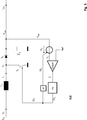
Fig. 2 Fig. 2
Fig. 3Fig. 3
Im Gegensatz zum Stand der Technik wird der Knoten dieses internen Spannungssignals (Vi) nun jedoch zusätzlich durch eine steuerbare Konstantstromquelle (IS) mit einem zeitlich in den Ladephasen konstanten elektrischen Ladestrom geladen bzw. mit einem zeitlich in den Entladephasen konstanten elektrischen Entladestrom entladen. Die Polarität des Ausgangsstroms der Konstantstromquelle (IS) hängt hierfür vom Wert des Schaltsignals (SS1), das den ersten Schalter (S1) steuert, ab. Durch diese dermaßen steuerbare Konstantstromquelle (Is) wird der Effekt des überlagerten Dreieckssignals auf dem zeitlichen Potenzialverlauf am Spannungsausgang (Vout) nun auf dem internen Spannungssignal (Vi) emuliert, sodass das interne Spannungssignal nun im Gegensatz zum Potenzialverlauf am Spannungsausgang (Vout) ein überlagertes Dreieckssignal zusätzlich aufweist. Dies ist ein wesentlicher erfindungsgemäßer Schritt. Eine Möglichkeit zur Realisierung der bipolaren gesteuerten Konstantstromquelle (Is) ist die Kombination einer nicht steuerbaren Konstantstromquelle (I1) mit einer in Abhängigkeit vom Schaltsignal (SS1) schaltbaren steuerbaren Konstantstromquelle (Is2) an Stelle der bipolaren gesteuerten Konstantstromquelle (Is), die dann nur eine der Konstantstromquelle (I1) entgegengesetzte Strompolarität bei einem doppelt so großem Strombetrag liefert. Stattdessen ist es auch denkbar, die nicht steuerbare Konstantstromquelle (I1) durch eine erste schaltbare Konstantstromquelle (IS1) zu ersetzen und diese gegentaktig zur zweiten schaltbaren steuerbaren Konstantstromquelle (Is2) anstelle der bipolaren, gesteuerten Konstantstromquelle (Is) in Abhängigkeit vom Schaltsignal (SS1) zu betreiben. Selbstverständlich sind andere Stromquellenkonfigurationen einer oder mehrerer Stromquellen denkbar, die im Ergebnis in Abhängigkeit vom Schaltsignal (SS1) einen im Ergebnis gleichen, in den Ladephasen konstanten Summenladestrom in den Knoten des internen Spannungssignals (Vi) einspeisen bzw. einen im Ergebnis gleichen, in den Entladephasen konstanten Summenentladestrom aus dem Knoten des internen Spannungssignals (Vi) entnehmen. In contrast to the prior art, however, the node of this internal voltage signal (V i ) is now additionally charged by a controllable constant current source (I S ) with a time constant in the charging phases electric charging current or discharged with a time constant in the discharge phases electric discharge. For this purpose, the polarity of the output current of the constant current source (I S ) depends on the value of the switching signal (SS 1 ) which controls the first switch (S 1 ). By means of this constant controllable constant current source (I s ), the effect of the superimposed triangular signal on the temporal potential curve at the voltage output (V out ) is now emulated on the internal voltage signal (V i ), so that the internal voltage signal now in contrast to the potential curve at the voltage output (V out ) additionally has a superimposed triangular signal. This is an essential step according to the invention. One possibility for realizing the bipolar controlled constant current source (I s ) is the combination of a non-controllable constant current source (I 1 ) with a controllable constant current source (I s2 ) which can be switched as a function of the switching signal (SS 1 ) instead of the bipolar controlled constant current source (I s ). , which then supplies only one of the constant current source (I 1 ) opposite current polarity at twice the current amount. Instead, it is also conceivable to replace the non-controllable constant-current source (I 1 ) by a first switchable constant-current source (I S1 ) and inverse-positive to the second switchable controllable constant current source (I s2 ) instead of the bipolar, controlled constant current source (I s ) as a function of Switching signal (SS 1 ) to operate. Of course, other current source configurations of one or more current sources are conceivable which, as a result, feed a cumulative charging current which is constant in the charging phases into the nodes of the internal voltage signal (V i ) as a function of the switching signal (SS 1 ) take the discharge phases constant Sumententladestrom from the node of the internal voltage signal (V i ).
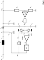
Fig. 4 Fig. 4
Der zweite Kondensator (Ci2) ist mit einem ersten Anschluss ebenfalls mit dem internen Spannungssignal (Ci) verbunden und mit dem zweiten Anschluss mit einem Bezugspotenzial. Die Einspeisung des zusätzlichen, überlagerten Dreieckssignals erfolgt nun aber nicht direkt durch die Konstantstromquellen (I1, Is) wie in
Statt einer nicht geschalteten Konstantstromquelle (I1) in Kombination mit einer steuerbaren Konstantstromquelle (Is), die ein- und ausgeschaltet wird, zur Erzeugung eines Lade- und Entladestroms in Abhängigkeit vom Schaltsignal (SS1) zum Laden und Entladen der Koppelkapazität (Ck) sind auch andere Realisierungen einer bipolaren Stromquelle denkbar. Stattdessen ist es beispielsweise auch denkbar, die nicht steuerbare Konstantstromquelle (I1) durch eine erste schaltbare Konstantstromquelle (IS1) zu ersetzen und diese gegentaktig zur zweiten schaltbaren steuerbaren Konstantstromquelle (Is2) anstelle der bipolaren, gesteuerten Konstantstromquelle (Is) in Abhängigkeit vom Schaltsignal (SS1) zu betreiben. Selbstverständlich sind andere Stromquellenkonfigurationen einer oder mehrerer Stromquellen denkbar, die im Ergebnis in Abhängigkeit vom Schaltsignal (SS1) einen im Ergebnis gleichen, in den Ladephasen konstanten Summenladestrom in den Knoten des internen Spannungssignals (Vi) einspeisen bzw. einen im Ergebnis gleichen, in den Entladephasen konstanten Summenentladestrom aus dem Knoten des internen Spannungssignals (Vi) entnehmen. Instead of a non-switched constant current source (I 1 ) in combination with a controllable constant current source (I s ), which is turned on and off, to generate a charging and discharging current in response to the switching signal (SS 1 ) for charging and discharging the coupling capacitance (C k ), other implementations of a bipolar current source are conceivable. Instead, it is also conceivable, for example, to replace the non-controllable constant current source (I 1 ) by a first switchable constant current source (I S1 ) and inverse-positive to the second switchable controllable constant current source (I s2 ) instead of the bipolar, controlled constant current source (I s ) in dependence to operate from the switching signal (SS 1 ). Of course, other current source configurations of one or more current sources are conceivable which, as a result, feed a cumulative charging current which is constant in the charging phases into the nodes of the internal voltage signal (V i ) as a function of the switching signal (SS 1 ) take the discharge phases constant Sumententladestrom from the node of the internal voltage signal (V i ).
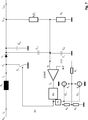
Fig. 5Fig. 5
Fig. 6Fig. 6
Im Gegensatz zum Stand der Technik wird der Knoten dieses internen Spannungssignals (Vi) nun jedoch zusätzlich durch eine steuerbare Konstantstromquelle (IS) geladen bzw. entladen, deren Polarität vom Wert des Schaltsignals (SS1), das den ersten Schalter (S1) steuert, abhängt. Ob der Knoten dieses internen Spannungssignals (Vi) durch die steuerbare Konstantstromquelle (IS) geladen oder entladen wird hängt also vom Wert des Schaltsignals (SS1) ab. Durch diese steuerbare Konstantstromquelle (Is) wird der Effekt des überlagerten Dreieckssignals auf dem zeitlichen Potenzialverlauf am Spannungsausgang (Vout) nun auf dem internen Spannungssignal (Vi) emuliert, sodass das interne Spannungssignal nun im Gegensatz zum Potenzialverlauf am Spannungsausgang (Vout) ein überlagertes Dreieckssignal zusätzlich aufweist. Dies ist ein wesentlicher erfindungsgemäßer Schritt. Eine Möglichkeit zur Realisierung der bipolaren gesteuerten Konstantstromquelle (Is) ist die Kombination einer nicht gesteuerten Konstantstromquelle (I1) mit einer schaltbaren steuerbaren Konstantstromquelle (Is), die dann nur eine der nicht gesteuerten Konstantstromquelle entgegengesetzte Strompolarität bei einem doppelt so großem Strombetrag liefert. In contrast to the prior art, however, the node of this internal voltage signal (V i ) is now additionally charged or discharged by a controllable constant current source (I S ) whose polarity is equal to the value of the switching signal (SS 1 ) connecting the first switch (S 1 ) controls, depends. Whether the node of this internal Voltage signal (V i ) is charged or discharged by the controllable constant current source (I S ) thus depends on the value of the switching signal (SS 1 ). The effect of the superimposed triangular wave on the temporal potential profile at the voltage output (V out) is now on the internal voltage signal (V i) by this controllable constant current source (I s) is emulated such that the internal voltage signal is now in contrast to the potential profile at the voltage output (V out) has a superimposed triangular signal in addition. This is an essential step according to the invention. One way to realize the bipolar controlled constant current source (I s ) is the combination of a non-controlled constant current source (I 1 ) with a switchable controllable constant current source (I s ), which then provides only one of the non-controlled constant current source opposite current polarity at twice the current amount ,
Fig. 7Fig. 7
Der zweite Kondensator (Ci2) des kapazitiven Spannungsteilers (Ci1, Ci2) ist mit einem ersten Anschluss ebenfalls mit dem internen Spannungssignal (Vi) verbunden und mit dem zweiten Anschluss mit einem Bezugspotenzial. Die Einspeisung des zusätzlichen, überlagerten Dreieckssignals erfolgt nun aber nicht direkt durch die Stromquellen (I1, Is) wie in
Statt einer nicht geschalteten Konstantstromquelle (I1) in Kombination mit einer steuerbaren Konstantstromquelle (Is), die ein- und ausgeschaltet wird, zur Erzeugung eines Lade- und Entladestroms in Abhängigkeit vom Schaltsignal (SS1) zum Laden und Entladen der Koppelkapazität (Ck) sind auch andere Realisierungen einer bipolaren Stromquelle denkbar. Stattdessen ist es beispielsweise auch denkbar, die nicht steuerbare Konstantstromquelle (I1) durch eine erste schaltbare Konstantstromquelle (IS1) zu ersetzen und diese gegentaktig zur zweiten schaltbaren steuerbaren Konstantstromquelle (Is2) anstelle der bipolaren, gesteuerten Konstantstromquelle (Is) in Abhängigkeit vom Schaltsignal (SS1) zu betreiben. Selbstverständlich sind andere Stromquellenkonfigurationen einer oder mehrerer Stromquellen denkbar, die im Ergebnis in Abhängigkeit vom Schaltsignal (SS1) einen im Ergebnis gleichen, in den Ladephasen konstanten Summenladestrom in den Knoten des internen Spannungssignals (Vi) einspeisen bzw. einen im Ergebnis gleichen, in den Entladephasen konstanten Summenentladestrom aus dem Knoten des internen Spannungssignals (Vi) entnehmen. Instead of a non-switched constant current source (I 1 ) in combination with a controllable constant current source (I s ), which is turned on and off, to generate a charging and discharging current in response to the switching signal (SS 1 ) for charging and discharging the coupling capacitance (C k ), other implementations of a bipolar current source are conceivable. Instead, it is also conceivable, for example, to replace the non-controllable constant current source (I 1 ) by a first switchable constant current source (I S1 ) and inverse-positive to the second switchable controllable constant current source (I s2 ) instead of the bipolar, controlled constant current source (I s ) in dependence to operate from the switching signal (SS 1 ). Of course, other current source configurations of one or more current sources are conceivable which, as a result, feed a cumulative charging current which is constant in the charging phases into the nodes of the internal voltage signal (V i ) as a function of the switching signal (SS 1 ) take the discharge phases constant Sumententladestrom from the node of the internal voltage signal (V i ).
Fig. 8Fig. 8
BezugszeichenlisteLIST OF REFERENCE NUMBERS
-
- ADCADC
- Analog-Digital-Wandler Analog to digital converter
- BufBuf
- Pufferschaltung buffer circuit
- C1 C 1
- Speicherkapazität. Hierbei kann es sich auch um mehrere Speicherkapazitäten handeln, die mit einem Anschluss mit dem Spannungsausgang (Vout) direkt oder indirekt verbunden sind und mit dem anderen Spannungsausgang mit einem Bezugspotenzial verbunden sind. Storage capacity. This can also be a plurality of storage capacities, which are connected directly or indirectly to one terminal to the voltage output (V out ) and are connected to a reference potential with the other voltage output.
- Ci C i
- Kondensator capacitor
- Ci1 C i1
- erster Kondensator. Der erste Kondensator bildet mit dem zweiten Kondensator (Ci2) einen kapazitiven Spannungsteiler parallel zum ohmschen Spannungsteiler (R1, R2) aus dem ersten Spannungsteilerwiderstand (R1) und dem zweiten Spannungsteilerwiderstand (R2). Durch diesen kapazitiven Spannungsteiler kann das Potenzial des internen Spannungssignals (Vi) schnell Spannungssprüngen der Ausgangsspannung am Spannungsausgang (Vout) folgen. first capacitor. The first capacitor forms with the second capacitor (C i2 ) a capacitive voltage divider parallel to the ohmic voltage divider (R 1 , R 2 ) from the first voltage divider resistor (R 1 ) and the second voltage divider resistor (R 2 ). By means of this capacitive voltage divider, the potential of the internal voltage signal (V i ) can quickly follow voltage jumps in the output voltage at the voltage output (V out ).
- Ci2 C i2
- zweiter Kondensator second capacitor
- Ck C k
- Koppelkapazität coupling capacitance
- Cs C s
- Komparatorausgangssignal comparator
- COMPCOMP
- Komparator comparator
- Δt.delta.t
- Verzögerungseinheit. Die Verzögerungseinheit verzögert das Schaltsignal (SS1) zum verzögerten Schaltsignal (SSv), um das aufgrund der Größe des ersten oder zweiten Schalters (S1, S2) verzögerte Schaltverhalten des ersten Schalters (S1) und/oder des zweiten Schalters (S2) für die Regelung zu berücksichtigen. Hierdurch wird die Erzeugung des Ripples auf dem internen Spannungssignal (Vi) zeitmäßig optimiert. Vorzugsweise wird die Verzögerungseinheit als Hintereinanderschaltung eines RC-Tiefpasses und eines Komparators oder Schmidt-Triggers realisiert. Delay unit. The delay unit delays the switching signal (SS 1 ) to the delayed switching signal (SS v ) to the delayed due to the size of the first or second switch (S1, S2) switching behavior of the first switch (S1) and / or the second switch (S 2 ) to be considered for the scheme. As a result, the generation of the ripples on the internal voltage signal (V i ) is optimized in terms of time. Preferably, the delay unit is implemented as a series connection of an RC low-pass filter and a comparator or Schmidt trigger.
- I1 I 1
- nicht steuerbare Konstantstromquelle. Diese liefert einen zeitlich konstanten elektrischen Strom. Sie wird vorzugsweise mit einer schaltbaren bipolaren Stromquelle kombiniert. non-controllable constant current source. This supplies a temporally constant electric current. It is preferably combined with a switchable bipolar current source.
- Iin I in
- Eingangsstrom input current
- IL I L
- Spulenstrom durch die Drosselspule (L1) Coil current through the choke coil (L 1 )
- IBuf I buf
- Ausgangsstrom der Pufferschaltung (Buf) Output current of the buffer circuit (Buf)
- Iout I out
- Ausgangsstrom output current
- IR I R
- Spannungsteilerstrom durch den ersten Spannungsteilerwiderstand (R1) und den zweiten Spannungsteilerwiderstand (R2) des Spannungsteilers (R1, R2) Voltage divider current through the first voltage divider resistor (R 1 ) and the second voltage divider resistor (R 2 ) of the voltage divider (R 1 , R 2 )
- Is I s
- steuerbare Konstantstromquelle. Die Steuerbarkeit bezieht sich dabei auf das Umschalten der Polarität des zeitlich betragsmäßig konstanten Ausgangsstromes der Konstantstromquelle. Die Stromquelle verhält sich also in den Zeiten zwischen den Umschaltungen wie eine Konstantstromquelle. controllable constant current source. The controllability refers to the switching of the polarity of the temporally magnitude constant output current of the constant current source. The current source thus behaves in the times between the switching as a constant current source.
- Is1 I s1
- erste steuerbare Konstantstromquelle. Die Steuerbarkeit bezieht sich dabei auf das Ein- bzw. Ausschalten eines in der Einschaltphase zeitlich konstanten elektrischen Ausgangsstroms der Konstantstromquelle. Die Stromquelle verhält sich also in den Zeiten zwischen den Schaltungen wie eine Konstantstromquelle. first controllable constant current source. The controllability refers to the switching on or off of a constant in the switch-on phase electrical output current of the constant current source. The current source thus behaves like a constant current source in the times between the circuits.
- Is2 I s2
- zweite steuerbare Konstantstromquelle. Die Steuerbarkeit bezieht sich dabei auf das Ein- bzw. Ausschalten eines in der Einschaltphase zeitlich konstanten elektrischen Ausgangsstroms der Konstantstromquelle. Die Stromquelle verhält sich also in den Zeiten zwischen den Schaltungen wie eine Konstantstromquelle. second controllable constant current source. The controllability refers to the switching on or off of a constant in the switch-on phase electrical output current of the constant current source. The current source thus behaves like a constant current source in the times between the circuits.
- Is3 I s3
- dritte steuerbare Konstantstromquelle. Die Steuerbarkeit bezieht sich dabei auf das Umschalten der Polarität des zeitlich betragsmäßig konstanten Ausgangsstromes der Konstantstromquelle. Die Stromquelle verhält sich also in den Zeiten zwischen den Umschaltungen wie eine Konstantstromquelle. third controllable constant current source. The controllability refers to the switching of the polarity of the temporally magnitude constant output current of the constant current source. The current source thus behaves in the times between the switching as a constant current source.
- L1 L 1
- Drosselspule inductor
- NBNB
- nicht beansprucht unclaimed
- PVPV
- Pulsverlängerungseinheit Pulse lengthening unit
- R1 R 1
- erster Spannungsteilerwiderstand first voltage divider resistor
- R2 R 2
- zweiter Spannungsteilerwiderstand second voltage divider resistor
- R3 R 3
- erster Arbeitspunktwiderstand first bias resistor
- R4 R 4
- zweiter Arbeitspunktwiderstand second working point resistance
- Ra R a
- Ausgangswiderstand der Pufferschaltung (Buf) Output resistance of the buffer circuit (Buf)
- Rs R s
- Vorwiderstand dropping resistor
- RefRef
- Referenzspannung reference voltage
- RESR R ESR
- Widerstand für die Stabilität des Regelkreises im Stand der Technik, der seriell zur Speicherkapazität (C1) geschaltet ist. Resistor for the stability of the control loop in the prior art, which is connected in series to the storage capacity (C 1 ).
- S1 S 1
- erster Schalter zwischen dem Spannungseingang (Vin) und dem Zwischenknoten (Z1) first switch between the voltage input (V in ) and the intermediate node (Z 1 )
- S2 S 2
- zweiter Schalter zwischen dem Zwischenknoten (Z1) und dem Spannungsausgang (Vout) second switch between the intermediate node (Z 1 ) and the voltage output (V out )
- SS1 SS 1
- Schaltsignal mit einer Schaltperiode TP Switching signal with a switching period T P
- SSv SS v
- verzögertes Schaltsignal delayed switching signal
- TA T A
- Aus-Zeit Off time
- TE T E
- Ein-Zeit One-time
- TP T P
- Schaltperiode; Dabei gilt TP = TA + TE. Switching period; Where T P = T A + T E.
- Vi V i
- internes Spannungssignal internal voltage signal
- Vin V in
- Spannungseingang voltage input
- Voff V off
- Spannungsoffset voltage offset
- Vout V out
- Spannungsausgang voltage output
- Z1 Z 1
- Zwischenknoten between nodes
Claims (5)
Applications Claiming Priority (2)
| Application Number | Priority Date | Filing Date | Title |
|---|---|---|---|
| DE102016104015.0 | 2016-03-06 | ||
| DE102016104015 | 2016-03-06 |
Publications (1)
| Publication Number | Publication Date |
|---|---|
| DE102016118932B3 true DE102016118932B3 (en) | 2017-02-09 |
Family
ID=57853917
Family Applications (1)
| Application Number | Title | Priority Date | Filing Date |
|---|---|---|---|
| DE102016118932.4A Active DE102016118932B3 (en) | 2016-03-06 | 2016-10-06 | DC buck converter |
Country Status (1)
| Country | Link |
|---|---|
| DE (1) | DE102016118932B3 (en) |
Citations (2)
| Publication number | Priority date | Publication date | Assignee | Title |
|---|---|---|---|---|
| US20130099761A1 (en) * | 2011-10-20 | 2013-04-25 | Yan Dong | Switching-Mode Power Supply with Ripple Mode Control and Associated Methods |
| US8698469B1 (en) * | 2011-09-12 | 2014-04-15 | Maxim Integreated Products, Inc. | System and method for predicting output voltage ripple and controlling a switched-mode power supply |
-
2016
- 2016-10-06 DE DE102016118932.4A patent/DE102016118932B3/en active Active
Patent Citations (2)
| Publication number | Priority date | Publication date | Assignee | Title |
|---|---|---|---|---|
| US8698469B1 (en) * | 2011-09-12 | 2014-04-15 | Maxim Integreated Products, Inc. | System and method for predicting output voltage ripple and controlling a switched-mode power supply |
| US20130099761A1 (en) * | 2011-10-20 | 2013-04-25 | Yan Dong | Switching-Mode Power Supply with Ripple Mode Control and Associated Methods |
Non-Patent Citations (1)
| Title |
|---|
| C.C. CHUANG; H.P. CHOU; M.L. CHIUA Buck Converter Using Accurate Synthetic Ripple Hysteresis Control SchemeIn: IEEE PEDS 2011, Singapore, 5-8 December 2011; p. 682 - 686 * |
Similar Documents
| Publication | Publication Date | Title |
|---|---|---|
| DE102015108822B4 (en) | System and method for current sampling in a switched-mode power supply | |
| DE102016207918B4 (en) | Multi-phase switching converter and method of operating a multi-phase switching converter | |
| DE102010009039B4 (en) | Methods and control circuits for controlling DC-DC converter circuits to produce a regulated output voltage with reduced average inductor current | |
| DE19814681B4 (en) | Current Mode Switching Regulators | |
| DE60224896T2 (en) | Circuits and methods for synchronizing non-constant frequency switching regulators by a phase locked loop | |
| DE102017205650A1 (en) | Feedback voltage DC level suppression for DC-DC switching converters with configurable output | |
| DE102015221414B4 (en) | Circuit and method for limiting the maximum duty cycle in upconverters | |
| DE102015226526B4 (en) | High-efficiency DC-to-DC converter with adaptive output stage | |
| DE112005000026T5 (en) | DC-DC converter and converter device | |
| DE102012107148A1 (en) | Digital control for DC / DC voltage transformers | |
| DE3713540A1 (en) | COMBINED SECONDARY SWITCH | |
| DE102017212349B4 (en) | Step-down converter (buck-boost) converter with hysteresis | |
| DE102016214446B4 (en) | Hybrid downshift | |
| DE10225406A1 (en) | Switch triggering method comparing threshold signal with ramp signal and triggering switch depending on result | |
| DE102009041217A1 (en) | Voltage transformer and voltage conversion method | |
| DE112019004487T5 (en) | ADAPTIVE EDGE COMPENSATION FOR CURRENT MODE CONTROL | |
| DE102005002570A1 (en) | Control circuit for buck converter, has signal converter designed so that absolute difference value between one control signal and amplitude value of sinusoidal signal relates to difference of another signal and amplitude value | |
| DE69921093T2 (en) | In a frequency converter used as a voltage regulator and battery charger DC converter and method for this frequency conversion | |
| DE102018216156A1 (en) | DOWN UP SWITCHING REGULATOR | |
| DE102016110670B4 (en) | Charge injection for immediate transient support | |
| DE102014103433B4 (en) | DIGITAL-ANALOG CONVERTER | |
| DE102017223883A1 (en) | Switching converter control with ruggedness against ESL ripple | |
| DE102016220199A1 (en) | DC-DC converter and method for operating a DC-DC converter | |
| DE102010036421A1 (en) | Overcurrent protection for DC-DC converters | |
| DE102016118932B3 (en) | DC buck converter |
Legal Events
| Date | Code | Title | Description |
|---|---|---|---|
| R012 | Request for examination validly filed | ||
| R018 | Grant decision by examination section/examining division | ||
| R020 | Patent grant now final | ||
| R081 | Change of applicant/patentee |
Owner name: ELMOS SEMICONDUCTOR SE, DE Free format text: FORMER OWNER: ELMOS SEMICONDUCTOR AKTIENGESELLSCHAFT, 44227 DORTMUND, DE |