DE102013112552B4 - Circuit arrangement and method for securing a circuit arrangement against repeated light attacks - Google Patents
Circuit arrangement and method for securing a circuit arrangement against repeated light attacks Download PDFInfo
- Publication number
- DE102013112552B4 DE102013112552B4 DE102013112552.2A DE102013112552A DE102013112552B4 DE 102013112552 B4 DE102013112552 B4 DE 102013112552B4 DE 102013112552 A DE102013112552 A DE 102013112552A DE 102013112552 B4 DE102013112552 B4 DE 102013112552B4
- Authority
- DE
- Germany
- Prior art keywords
- line
- circuit arrangement
- circuit
- arrangement according
- light
- Prior art date
- Legal status (The legal status is an assumption and is not a legal conclusion. Google has not performed a legal analysis and makes no representation as to the accuracy of the status listed.)
- Active
Links
Images
Classifications
-
- G—PHYSICS
- G06—COMPUTING OR CALCULATING; COUNTING
- G06F—ELECTRIC DIGITAL DATA PROCESSING
- G06F21/00—Security arrangements for protecting computers, components thereof, programs or data against unauthorised activity
- G06F21/70—Protecting specific internal or peripheral components, in which the protection of a component leads to protection of the entire computer
- G06F21/71—Protecting specific internal or peripheral components, in which the protection of a component leads to protection of the entire computer to assure secure computing or processing of information
- G06F21/76—Protecting specific internal or peripheral components, in which the protection of a component leads to protection of the entire computer to assure secure computing or processing of information in application-specific integrated circuits [ASIC] or field-programmable devices, e.g. field-programmable gate arrays [FPGA] or programmable logic devices [PLD]
-
- H—ELECTRICITY
- H10—SEMICONDUCTOR DEVICES; ELECTRIC SOLID-STATE DEVICES NOT OTHERWISE PROVIDED FOR
- H10W—GENERIC PACKAGES, INTERCONNECTIONS, CONNECTORS OR OTHER CONSTRUCTIONAL DETAILS OF DEVICES COVERED BY CLASS H10
- H10W42/00—Arrangements for protection of devices
- H10W42/40—Arrangements for protection of devices protecting against tampering, e.g. unauthorised inspection or reverse engineering
- H10W42/405—Arrangements for protection of devices protecting against tampering, e.g. unauthorised inspection or reverse engineering using active circuits
-
- G—PHYSICS
- G06—COMPUTING OR CALCULATING; COUNTING
- G06F—ELECTRIC DIGITAL DATA PROCESSING
- G06F21/00—Security arrangements for protecting computers, components thereof, programs or data against unauthorised activity
- G06F21/50—Monitoring users, programs or devices to maintain the integrity of platforms, e.g. of processors, firmware or operating systems
- G06F21/55—Detecting local intrusion or implementing counter-measures
- G06F21/556—Detecting local intrusion or implementing counter-measures involving covert channels, i.e. data leakage between processes
-
- G—PHYSICS
- G06—COMPUTING OR CALCULATING; COUNTING
- G06F—ELECTRIC DIGITAL DATA PROCESSING
- G06F21/00—Security arrangements for protecting computers, components thereof, programs or data against unauthorised activity
- G06F21/70—Protecting specific internal or peripheral components, in which the protection of a component leads to protection of the entire computer
- G06F21/71—Protecting specific internal or peripheral components, in which the protection of a component leads to protection of the entire computer to assure secure computing or processing of information
- G06F21/75—Protecting specific internal or peripheral components, in which the protection of a component leads to protection of the entire computer to assure secure computing or processing of information by inhibiting the analysis of circuitry or operation
- G06F21/755—Protecting specific internal or peripheral components, in which the protection of a component leads to protection of the entire computer to assure secure computing or processing of information by inhibiting the analysis of circuitry or operation with measures against power attack
-
- H—ELECTRICITY
- H10—SEMICONDUCTOR DEVICES; ELECTRIC SOLID-STATE DEVICES NOT OTHERWISE PROVIDED FOR
- H10W—GENERIC PACKAGES, INTERCONNECTIONS, CONNECTORS OR OTHER CONSTRUCTIONAL DETAILS OF DEVICES COVERED BY CLASS H10
- H10W42/00—Arrangements for protection of devices
- H10W42/20—Arrangements for protection of devices protecting against electromagnetic or particle radiation, e.g. light, X-rays, gamma-rays or electrons
Landscapes
- Engineering & Computer Science (AREA)
- Computer Hardware Design (AREA)
- Theoretical Computer Science (AREA)
- Physics & Mathematics (AREA)
- Computer Security & Cryptography (AREA)
- Software Systems (AREA)
- General Engineering & Computer Science (AREA)
- General Physics & Mathematics (AREA)
- Mathematical Physics (AREA)
- Microelectronics & Electronic Packaging (AREA)
- Semiconductor Integrated Circuits (AREA)
- Health & Medical Sciences (AREA)
- Electromagnetism (AREA)
- Toxicology (AREA)
Abstract
Schaltungsanordnung (100) aufweisend eine Detektionsschaltung (101), die eingerichtet ist, Lichtangriffe auf die Schaltungsanordnung (100) zu detektieren; eine Verarbeitungsschaltung (102), die eingerichtet ist, für jeden durch die Detektionsschaltung (101) detektierten Lichtangriff einen Stromfluss durch eine Leitung (103) zu veranlassen, wobei bei Überschreiten einer gewissen Anzahl durch Lichtangriffe veranlasster Stromflüsse die Leitung (103) zerstört wird oder eine Leitfähigkeit der Leitung (103) um einen gewissen Betrag verringert wird; und eine Steuerschaltung (104), die eingerichtet ist, abhängig vom Leitzustand der Leitung (103) die Funktion einer Komponente (105) der Schaltungsanordnung (100) zu ermöglichen, wobei der Leitzustand im Funktionszustand der Leitung (103) die Leitfähigkeit der Leitung ist; und wobei die Steuerschaltung (104) eingerichtet ist, die Funktion der Komponente (105) der Schaltungsanordnung (100) zu verhindern, wenn die Leitfähigkeit der Leitung (103) unter einem vorgegebenen Wert ist.Circuit arrangement (100) comprising a detection circuit (101) which is set up to detect light attacks on the circuit arrangement (100); a processing circuit (102) which is set up to cause a current flow through a line (103) for each light attack detected by the detection circuit (101), the line (103) being destroyed or being exceeded when a certain number of current flows induced by light attacks are exceeded Conductivity of the line (103) is reduced by a certain amount; and a control circuit (104) arranged to enable the function of a component (105) of the circuit arrangement (100), depending on the conduction state of the line (103), the conduction state in the functional state of the line (103) being the conductivity of the line; and wherein the control circuit (104) is arranged to prevent the function of the component (105) of the circuit arrangement (100) when the conductivity of the line (103) is below a predetermined value.
Description
Ausführungsbeispiele betreffen allgemein Schaltungsanordnungen und Verfahren zum Sichern einer Schaltungsanordnung gegen wiederholte Lichtangriffe.Embodiments relate generally to circuitry and methods for securing a circuit against repetitive light attacks.
Integrierte Schaltungen, die für sicherheitskritische Anwendungen verwendet werden, beispielsweise auf Chipkarten, sollen typischerweise gegen Angriffe geschützt werden. Ein Typ solcher Angriffe sind Lichtangriffe, typischerweise Laserattacken, bei denen eine Funktionsstörung eines Bauelements bewirkt werden soll. Es ist insbesondere wünschenswert, die zeitliche und räumliche Wiederholbarkeit solcher Fehlerangriffe einzuschränken.
Die Figuren geben nicht die tatsächlichen Größenverhältnisse wieder sondern sollen dazu dienen, die Prinzipien der verschiedenen Ausführungsbeispiele zu illustrieren. Im Folgenden werden verschiedene Ausführungsbeispiele mit Bezug auf die folgenden Figuren beschrieben.The figures do not reflect the actual proportions but are intended to illustrate the principles of the various embodiments. In the following, various embodiments will be described with reference to the following figures.
Die folgende detaillierte Beschreibung bezieht sich auf die beiliegenden Figuren, die Details und Ausführungsbeispiele zeigen. Diese Ausführungsbeispiele sind so detailliert beschrieben, dass der Fachmann die Erfindung ausführen kann. Andere Ausführungsformen sind auch möglich und die Ausführungsbeispiele können in struktureller, logischer und elektrischer Hinsicht geändert werden, ohne vom Gegenstand der Erfindung abzuweichen. Die verschiedenen Ausführungsbeispiele schließen sich nicht notwendig gegenseitig aus sondern es können verschiedene Ausführungsformen miteinander kombiniert werden, so dass neue Ausführungsformen entstehen.The following detailed description refers to the accompanying figures which show details and embodiments. These embodiments are described in such detail that those skilled in the art can practice the invention. Other embodiments are also possible and the embodiments may be changed in structural, logical and electrical terms without departing from the subject matter of the invention. The various embodiments are not necessarily mutually exclusive, but various embodiments may be combined to form new embodiments.
Registrieren von Lichtangriffen durch Felder mit nichtflüchtigen Speicherzellen mit eigener Peripherie ermöglicht nur begrenzten Schutz gegen wiederholte Lichtangriffe.Registering light attacks by fields with non-volatile memory cells with their own peripherals provides only limited protection against repeated light attacks.
Typischerweise werden nur wenige der Angriffe mittels einer begrenzten Anzahl lokal implementierter Sensorelemente erkannt und eine flächendeckende Erkennung der Angriffe ist nicht möglich.Typically, only a few of the attacks are detected by means of a limited number of locally implemented sensor elements and blanket detection of the attacks is not possible.
Erfolgen Attacken außerdem in schneller Abfolge, so wird dies typischerweise nicht erkannt und (aufgrund der erforderlichen Speicher-Programmierzeit) nur ein Teil der Attacken registriert.In addition, if attacks occur in rapid succession, this is typically not detected and only a fraction of the attacks are registered (due to the required memory programming time).
Erzeugt eine Attacke auf Grund ihrer großen Intensität einen Latchup in dem angegriffenen Chip, so ist die Chipfunktionalität nicht mehr gegeben, die den Ablauf der erforderlichen Speicherzellen-Programmierung zuverlässig steuern kann.If an attack generates a latchup in the attacked chip due to its high intensity, the chip functionality that can reliably control the execution of the required memory cell programming no longer exists.
Außerdem ist diese Herangehensweise mittels spezieller Speicherzellenfelder typischerweise sehr flächenintensiv, da ein gesondertes Speicherzellenfeld und weitere Komponente (z. B. Ladungspumpen etc.) vorgesehen werden müssen.In addition, this approach using special memory cell arrays is typically very area-intensive, as a separate memory cell array and other components (eg, charge pumps, etc.) must be provided.
Im Folgenden wird eine Ausführungsform beschrieben, bei der die Zahl der Licht-Fehlerangriffe im Unterschied zu der oben beschriebenen Herangehensweise mittels einer Metallleitung registriert wird.In the following, an embodiment will be described in which the number of light failures is registered by means of a metal line unlike the above-described approach.
Die Schaltungsanordnung weist eine Detektionsschaltung
Die Schaltungsanordnung weist außerdem eine Steuerschaltung
In anderen Worten: Es werden gemäß einer Ausführungsform Fehlerangriffe (in Form lokaler Lichtangriffe) auf eine Schaltungsanordnung, beispielsweise einen Chip, mittels einer Leitung registriert, indem, beispielsweise für jeden detektierten Lichtangriff ein Stromfluss (ausreichender Stärke) durch die Leitung erzeugt wird. Die Leitung ist beispielsweise derart ausgestaltet, dass sie bei jedem auf diese Weise verursachten Stromfluss derart altert, dass Sie nach einer vorgegebenen Zahl (z. B. in einem gewissen Zahlbereich, da die Alterung typischerweise nicht exakt vorhergesagt werden kann) von detektierten Lichtangriffen und entsprechenden Stromflüssen durch die Leitung ihre Leitfähigkeit verliert, beispielsweise durchbrennt oder durchschmilzt (es handelt sich beispielsweise um eine, gemessen an dem veranlassten Stromfluss, dünne Leitung, d. h. eine Leitung, die nicht geeignet ist, einen Strom der Größe, wie er erzeugt wird, dauerhaft zu verkraften). Nach Durchbrennen der Leitung ermöglicht die Steuerschaltung beispielsweise die Funktion bestimmter Komponenten der Schaltungsanordnung nicht mehr. Beispielsweise können eine oder mehrere Komponenten des Chips, beispielsweise eine zentrale Verarbeitungseinheit, nicht mehr gestartet werden.In other words, according to an embodiment, fault attacks (in the form of local light attacks) are registered on a circuit arrangement, for example a chip, by means of a line, for example by generating a current flow (sufficient strength) through the line for each detected light attack. For example, the line is designed to age with each current flow so caused to fall off a detected number (eg, in a certain number range, as aging typically can not be accurately predicted) of detected light attacks and the like Current flows through the line loses its conductivity, for example, burns or melts (it is, for example, a, measured on the induced current flow, thin line, ie a line that is not suitable, a stream of the size as it is generated permanently cope). After blowing through the line, the control circuit, for example, no longer allows the function of certain components of the circuit arrangement. For example, one or more components of the chip, for example a central processing unit, can no longer be started.
In anderen Worten: Es erfolgt durch die veranlassten Stromflüsse durch die Leitung eine Integralbildung der detektierten Lichtangriffe, die, bei Überschreiten einer gewissen Zahl (die die Leitung zerstört oder allgemein ihre Leitfähigkeit um einen gewissen Betrag verringert), zu einer beispielsweise dauerhaften Blockade von ein oder mehreren Komponenten oder des gesamten Chips führt.In other words, by the induced current flows through the line an integral formation of the detected light attacks, which, when a certain number is exceeded (which destroys the line or generally their conductivity by a certain amount), for example, a permanent blockade of on or multiple components or the entire chip leads.
Für diese Herangehensweise ist kein Programmiervorgang erforderlich und sie kann mit geringer Komplexität und geringem Flächenaufwand realisiert werden (beispielsweise ist kein zusätzliches Speicherzellenfeld und weitere Komponenten zum Betrieb der zusätzlichen Speicherzellen erforderlich).No programming is required for this approach, and it can be implemented with low complexity and low area overhead (eg, no additional memory cell array and other components are required to operate the additional memory cells).
Da erwartet werden kann, dass die Zahl von Angriffen, nach der sich der Leitzustand der Leitung ändert (die Leitung beispielsweise durchbrennt) vom einzelnen Chip abhängt, kann bei mehreren Chips eine große Streuung der Zahl von Angriffen, nach der der Chip nicht mehr funktionsfähig ist, erwartet werden. Dies erschwert einem Angreifer das Verständnis der Vorgänge im Chip.Since it can be expected that the number of attacks after which the conduction state of the line changes (the line burns, for example) depends on the single chip, with multiple chips, there can be a large dispersion in the number of attacks after which the chip is no longer functional , to be expected. This makes it more difficult for an attacker to understand the processes in the chip.
Die einzelnen Attacken werden beispielsweise mittels eines Wannensensors erkannt. Das Durchbrennen (oder allgemein die Änderung des Leitzustands) der Leitung versetzt den Chip beispielsweise in einen permanenten Resetzustand, in dem kein Zugriff auf den Chip mehr möglich ist.The individual attacks are detected, for example, by means of a pan sensor. For example, blowing (or generally changing the conduction state) of the line puts the chip in a permanent reset state where access to the chip is no longer possible.
Gemäß einer Ausführungsform ist beispielsweise parallel zu der Leitung ein Schalter vorgesehen, so dass die Leitung überbrückt werden kann. Damit kann das Risiko minimiert werden, dass die Leitung ungewollt ihren Leitzustand ändert und der Chip ungewollt nicht mehr funktionsfähig ist. In anderen Worten: Es kann die Schaltungsanordnung dahingehend konfigurierbar sein, dass unabhängig vom Leitzustand der Leitung die Funktion der Komponente der Schaltungsanordnung ermöglicht wird.According to one embodiment, for example, a switch is provided parallel to the line, so that the line can be bridged. Thus, the risk can be minimized that the line unintentionally changes its conduction state and the chip is unintentionally no longer functional. In other words, the circuit arrangement can be configured in such a way that the function of the component of the circuit arrangement is made possible independently of the conduction state of the line.
Der Leitzustand ist beispielsweise die Leitfähigkeit der Leitung wenn sich die Leitung im Funktionszustand befindet, d. h. wenn die Leitung nicht aufgetrennt ist. Der Leitzustand kann auch einer fehlenden Leitfähigkeit der Leitung entsprechen, wenn sich die Leitung nicht im Funktionszustand befindet, z. B. wenn die Leitung aufgetrennt ist.The conduction state is, for example, the conductivity of the line when the line is in the functional state, i. E. H. if the line is not disconnected. The conduction state can also correspond to a lack of conductivity of the line when the line is not in the functional state, eg. B. when the line is disconnected.
Beispielsweise kann die Steuerschaltung die Funktion der Komponente der Schaltungsanordnung verhindern, wenn die Leitfähigkeit der Leitung unter einem vorgegebenen Wert ist.For example, the control circuit may prevent the function of the component of the circuit arrangement when the conductivity of the line is below a predetermined value.
Gemäß einer Ausführungsform kann die Steuerschaltung die Schaltungsanordnung in einen Reset-Zustand versetzen, wenn die Leitfähigkeit der Leitung unter einem vorgegebenen Wert ist.According to an embodiment, the control circuit may set the circuit arrangement in a reset state if the conductivity of the line is below a predetermined value.
Beispielsweise kann die Steuerschaltung die Funktion der Komponente der Schaltungsanordnung verhindern, wenn die Leitung aufgetrennt ist.For example, the control circuit may prevent the function of the component of the circuit arrangement when the line is disconnected.
Beispielsweise kann die Steuerschaltung die Schaltungsanordnung in einen Reset(Rücksetz)-Zustand versetzen, wenn die Leitung aufgetrennt ist.For example, the control circuitry may place the circuitry in a reset (reset) state when the line is disconnected.
Die Steuerschaltung kann beispielsweise abhängig vom Leitzustand der Leitung die Komponente aktivieren.For example, the control circuit may activate the component depending on the conduction state of the line.
In einer Ausführungsform weist die Schaltungsanordnung eine CMOS-Schaltung auf und die Detektionsschaltung ist eingerichtet, einen Lichtangriff auf die CMOS-Schaltung zu detektieren.In an embodiment, the circuit arrangement comprises a CMOS circuit and the detection circuit is configured to detect a light attack on the CMOS circuit.
Die Detektionsschaltung weist beispielsweise einen Wannensensor auf.The detection circuit has, for example, a tray sensor.
Gemäß einer Ausführungsform ist die Schaltungsanordnung ein Chip. According to one embodiment, the circuit arrangement is a chip.
Die Steuerschaltung ist beispielsweise eingerichtet, abhängig vom Leitzustand der Leitung den Chip zu starten oder in einem Rest-Zustand zu belassen.By way of example, the control circuit is set up to start or leave the chip in a residual state, depending on the conduction state of the line.
Gemäß einer Ausführungsform weist die Leitung einen Leitungspfad und einen zu dem Leitungspfad parallel geschalteten Schalter auf.According to one embodiment, the line has a conduction path and a switch connected in parallel with the conduction path.
Gemäß einer Ausführungsform ist die Detektionsschaltung derart eingerichtet, dass sie für jeden detektierten Lichtangriff auf die Schaltungsanordnung ein Signal ausgibt, das anzeigt, dass ein Lichtangriff detektiert wurde und die Verarbeitungsschaltung ist eingerichtet, bei Empfang des Signals einen Stromfluss durch eine Leitung zu veranlassen.According to one embodiment, the detection circuit is arranged to output a signal indicating that a light attack has been detected for each detected light attack on the circuitry, and the processing circuitry is adapted to cause current to flow through a line upon receipt of the signal.
Beispielsweise verbindet die Verarbeitungsschaltung in Reaktion auf den Empfang des Signals die Leitung mit ihrem einem Ende mit einem Knoten mit hohem Versorgungspotential und mit ihrem anderen Ende mit einem Knoten mit niedrigem Versorgungspotential.For example, in response to receiving the signal, the processing circuit connects the line at one end to a high supply potential node and at its other end to a low supply potential node.
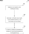
Die Schaltungsanordnung führt beispielsweise ein Verfahren durch, wie es in
Das Ablaufdiagramm
In
In
In
Es sollte beachtet werden, dass
Ausführungsbeispiele, die im Zusammenhang mit der Schaltungsanordnung
Im Folgenden werden Ausführungsbeispiele detaillierter beschrieben.In the following, embodiments will be described in more detail.
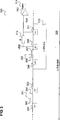
Gemäß einer Ausführungsform basiert die Detektionsschaltung auf der Detektion einer Spannungsänderung in einer Wanne. Ein Beispiel für eine entsprechende Detektionsschaltung wird im Folgenden mit Bezug auf
Die Detektionsanordnung ist in diesem Beispiel Teil eines Chips in CMOS-Technologie. Entsprechend weist der Chip eine Vielzahl von nMOS-Transistoren und eine Vielzahl von pMOS-Transistoren auf. Exemplarisch für diese Transistoren sind ein nMOS-Transistor
Der nMOS-Transistor
Analog weist der pMOS-Transistor
Der nMOS-Transistor
Der Wannenanschlussbereich
Da der Wannenanschlussbereich
Durch geeignete Wahl des Referenzpotentials kann somit ein Lichtangriff, der zum Entladen der n-Wanne
Typischerweise sind bei einem Chip in CMOS-Technologie in einer Wanne eine Vielzahl von Transistoren angeordnet. In anderen Worten, die n-Wanne
Lichtattacken mit kleinerer und mittlerer Amplitude auf den Chip können über die Absenkung des Wannenpotentials detektiert werden. Die Detektionsschaltung (d. h. die Anordnung aus Wannenanschlussbereich
Bei einer Lichtattacke mit (ausreichend) großer Amplitude, die die n-Wanne
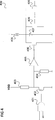
Ein Beispiel für eine Verarbeitungsschaltung und eine Steuerschaltung die beispielsweise das Alarmsignal
Die Schaltungsanordnung
Der Ausgang des UND-Gatters
In anderen Worten führt das zeitliche Integral aller Attacken zum Auftrennen der Leitung.In other words, the temporal integral of all attacks leads to the disconnection of the line.
Die Schaltung aus UND-Gatter
Der Drain-Anschluss des ersten nMOS-Transistors
Der Source-Anschluss des zweiten nMOS-Transistors
Ist hingegen die Leitung
In anderen Worten, dies führt zu einem dauerhaften POR(Power an Reset)-Zustand mit der Folge, dass der Chip nie mehr startet.In other words, this results in a permanent POR (Power on Reset) state, with the result that the chip never starts again.
Die Schaltungsanordnung weist außerdem Rücksetz-Pfade (Reset-Pfade) auf, mit denen der Chip in den POR-Zustand versetzt werden kann.The circuitry also includes reset paths that allow the chip to go into the POR state.
An Stelle eines Durchbrennens der Leitung
Claims (13)
Priority Applications (2)
| Application Number | Priority Date | Filing Date | Title |
|---|---|---|---|
| DE102013112552.2A DE102013112552B4 (en) | 2013-11-14 | 2013-11-14 | Circuit arrangement and method for securing a circuit arrangement against repeated light attacks |
| US14/541,258 US9552499B2 (en) | 2013-11-14 | 2014-11-14 | Circuit arrangement and method for safeguarding a circuit arrangement with respect to repeated light attacks |
Applications Claiming Priority (1)
| Application Number | Priority Date | Filing Date | Title |
|---|---|---|---|
| DE102013112552.2A DE102013112552B4 (en) | 2013-11-14 | 2013-11-14 | Circuit arrangement and method for securing a circuit arrangement against repeated light attacks |
Publications (2)
| Publication Number | Publication Date |
|---|---|
| DE102013112552A1 DE102013112552A1 (en) | 2015-05-21 |
| DE102013112552B4 true DE102013112552B4 (en) | 2017-05-24 |
Family
ID=53045050
Family Applications (1)
| Application Number | Title | Priority Date | Filing Date |
|---|---|---|---|
| DE102013112552.2A Active DE102013112552B4 (en) | 2013-11-14 | 2013-11-14 | Circuit arrangement and method for securing a circuit arrangement against repeated light attacks |
Country Status (2)
| Country | Link |
|---|---|
| US (1) | US9552499B2 (en) |
| DE (1) | DE102013112552B4 (en) |
Families Citing this family (5)
| Publication number | Priority date | Publication date | Assignee | Title |
|---|---|---|---|---|
| DE102015014403A1 (en) | 2015-11-06 | 2017-05-11 | Giesecke & Devrient Gmbh | Method and device for determining a zero point |
| FR3063597A1 (en) * | 2017-03-06 | 2018-09-07 | Stmicroelectronics (Rousset) Sas | ELECTRONIC CHIP ARCHITECTURE |
| US11316210B2 (en) | 2018-11-21 | 2022-04-26 | Samsung Sdi Co., Ltd. | Control unit for a battery module or system |
| KR102780357B1 (en) | 2020-01-07 | 2025-03-12 | 삼성전자주식회사 | Defense circuit of semiconductor device and semiconductor device including the same |
| US11121097B1 (en) * | 2020-05-22 | 2021-09-14 | Globalfoundries U.S. Inc. | Active x-ray attack prevention device |
Citations (8)
| Publication number | Priority date | Publication date | Assignee | Title |
|---|---|---|---|---|
| WO2000058807A1 (en) * | 1999-03-26 | 2000-10-05 | Infineon Technologies Ag | Manipulation-proof integrated circuit |
| WO2002017398A1 (en) * | 2000-08-21 | 2002-02-28 | Infineon Technologies Ag | Device for protecting an integrated circuit formed in a substrate |
| DE10345240A1 (en) * | 2003-09-29 | 2005-05-04 | Infineon Technologies Ag | Integrated circuit with radiation sensor arrangement |
| US20050236683A1 (en) * | 2002-06-04 | 2005-10-27 | Yigal Shapiro | Prevention of tampering in electronic devices |
| US7038307B2 (en) * | 2001-11-14 | 2006-05-02 | Infineon Technologies Ag | Semiconductor chip with FIB protection |
| US20060192681A1 (en) * | 2003-06-17 | 2006-08-31 | Infineon Technologies Ag | Circuit arrangement |
| DE102007058003A1 (en) * | 2007-12-03 | 2009-06-25 | Infineon Technologies Ag | Semiconductor component for recognition of light affect in smart card, has semiconductor substrate, semiconductor structure formed in semiconductor substrate and sensor element |
| DE102010045328A1 (en) * | 2010-09-14 | 2012-03-15 | Giesecke & Devrient Gmbh | Portable disk |
Family Cites Families (9)
| Publication number | Priority date | Publication date | Assignee | Title |
|---|---|---|---|---|
| DE10206186B4 (en) * | 2002-02-14 | 2010-01-28 | Infineon Technologies Ag | Memory matrix and method for securing a memory matrix |
| DE10254325A1 (en) * | 2002-11-21 | 2004-06-03 | Philips Intellectual Property & Standards Gmbh | Electronic memory component |
| KR100837275B1 (en) * | 2006-12-06 | 2008-06-11 | 삼성전자주식회사 | Smart card to detect light |
| KR101477630B1 (en) * | 2007-10-09 | 2014-12-30 | 삼성전자주식회사 | Memory device for detecting light attack and method thereof |
| FR2953960B1 (en) * | 2009-12-14 | 2012-01-13 | Oberthur Technologies | ELECTRONIC COMPONENT FOR DETECTING ATTACKS BY ENERGY DELIVERY |
| DE102011018450B4 (en) | 2011-04-21 | 2017-08-31 | Infineon Technologies Ag | Semiconductor device with through-connected parasitic thyristor in a light attack and semiconductor device with alarm circuit for a light attack |
| FR2981783B1 (en) * | 2011-10-19 | 2014-05-09 | St Microelectronics Rousset | SYSTEM FOR DETECTING A LASER ATTACK OF AN INTEGRATED CIRCUIT CHIP |
| FR2986633B1 (en) * | 2012-02-08 | 2014-09-05 | St Microelectronics Rousset | DEVICE FOR DETECTION OF LASER ATTACK IN AN INTEGRATED CIRCUIT CHIP |
| JP5939675B2 (en) * | 2012-04-20 | 2016-06-22 | ルネサスエレクトロニクス株式会社 | Semiconductor device and control system |
-
2013
- 2013-11-14 DE DE102013112552.2A patent/DE102013112552B4/en active Active
-
2014
- 2014-11-14 US US14/541,258 patent/US9552499B2/en active Active
Patent Citations (8)
| Publication number | Priority date | Publication date | Assignee | Title |
|---|---|---|---|---|
| WO2000058807A1 (en) * | 1999-03-26 | 2000-10-05 | Infineon Technologies Ag | Manipulation-proof integrated circuit |
| WO2002017398A1 (en) * | 2000-08-21 | 2002-02-28 | Infineon Technologies Ag | Device for protecting an integrated circuit formed in a substrate |
| US7038307B2 (en) * | 2001-11-14 | 2006-05-02 | Infineon Technologies Ag | Semiconductor chip with FIB protection |
| US20050236683A1 (en) * | 2002-06-04 | 2005-10-27 | Yigal Shapiro | Prevention of tampering in electronic devices |
| US20060192681A1 (en) * | 2003-06-17 | 2006-08-31 | Infineon Technologies Ag | Circuit arrangement |
| DE10345240A1 (en) * | 2003-09-29 | 2005-05-04 | Infineon Technologies Ag | Integrated circuit with radiation sensor arrangement |
| DE102007058003A1 (en) * | 2007-12-03 | 2009-06-25 | Infineon Technologies Ag | Semiconductor component for recognition of light affect in smart card, has semiconductor substrate, semiconductor structure formed in semiconductor substrate and sensor element |
| DE102010045328A1 (en) * | 2010-09-14 | 2012-03-15 | Giesecke & Devrient Gmbh | Portable disk |
Also Published As
| Publication number | Publication date |
|---|---|
| DE102013112552A1 (en) | 2015-05-21 |
| US9552499B2 (en) | 2017-01-24 |
| US20150135340A1 (en) | 2015-05-14 |
Similar Documents
| Publication | Publication Date | Title |
|---|---|---|
| DE102011018450B4 (en) | Semiconductor device with through-connected parasitic thyristor in a light attack and semiconductor device with alarm circuit for a light attack | |
| DE102016114740B3 (en) | Electronic fuse for an electrical load in a vehicle electrical system of a motor vehicle | |
| DE102013112552B4 (en) | Circuit arrangement and method for securing a circuit arrangement against repeated light attacks | |
| EP1714321B1 (en) | Circuit arrangement and method for protecting an integrated semiconductor circuit | |
| WO2009027348A2 (en) | Circuit arrangement for protection from electrostatic discharges and method for operating the same | |
| DE102011004774B4 (en) | Integrated circuit with a radiation-sensitive thyristor structure, chip card with radiation-sensitive thyristor structure and method for protecting against an attack on a security circuit | |
| DE102008006301B4 (en) | Circuit for detecting voltage changes and method for detecting a voltage change | |
| DE112013003667B4 (en) | sensor device | |
| DE112021003633T5 (en) | VOLTAGE GLITCH DETECTION AND PROTECTION CIRCUIT FOR SECURE STORAGE DEVICES | |
| DE102020104630B4 (en) | CROSS-DOMAIN VOLTAGE FAULT DETECTION CIRCUIT TO IMPROVE CHIP SECURITY | |
| DE102008006963B4 (en) | ESD power clamping device with stable switch-on function | |
| DE10214898A1 (en) | memory circuit | |
| DE102009055264B4 (en) | Digital fault detection circuit and method | |
| DE102014102623A1 (en) | Memory arrangement and method for detecting an attack on a memory array | |
| DE3630679C2 (en) | ||
| DE102017120944B4 (en) | Chip with circuitry for detecting an attack on the chip | |
| DE102013203076B4 (en) | Device with detection of the latch-up effect and method for forming this device | |
| DE102014107455B4 (en) | INTEGRATED CIRCUIT WITH LOGIC CIRCUIT FOR CHECKING POTENTIAL DIFFERENCES IN A CONNECTION AREA AND METHOD FOR DETECTING AN ATTACK ON AN INTEGRATED CIRCUIT | |
| DE112021003078T5 (en) | DETECTION OF FAULT INJECTION EVENTS AT A CHIP AND RELATED SYSTEMS, METHODS AND DEVICES | |
| DE102019116468B3 (en) | Integrated circuit with detection circuit and associated chip card | |
| DE102019105249B4 (en) | INTEGRATED CIRCUIT | |
| DE102020107479A1 (en) | Apparatus and method for preventing undamaged airbag ignition circuits from failing in the event of an accident | |
| DE102009039247B4 (en) | Semiconductor body with a connection cell | |
| DE112014006383T5 (en) | Detection of dependent failures | |
| EP1128248A1 (en) | Semiconductor chip with a light sensitive element |
Legal Events
| Date | Code | Title | Description |
|---|---|---|---|
| R012 | Request for examination validly filed | ||
| R016 | Response to examination communication | ||
| R016 | Response to examination communication | ||
| R018 | Grant decision by examination section/examining division | ||
| R020 | Patent grant now final | ||
| R082 | Change of representative | ||
| R079 | Amendment of ipc main class |
Free format text: PREVIOUS MAIN CLASS: H01L0023580000 Ipc: H10W0029000000 |