HINTERGRUND DER ERFINDUNGBACKGROUND OF THE INVENTION
Gebietarea
Ausführungsformen der Erfindung betreffen elektronische Systeme und insbesondere Fehlerschutzsysteme für Verstärker.Embodiments of the invention relate to electronic systems, and more particularly to error protection systems for amplifiers.
Beschreibung verwandter TechnologieDescription of related technology
Bestimmte Verstärker können einer Fehlerbedingung ausgesetzt sein, bei welcher der Spannungspegel eines Pols des Verstärkers außerhalb eines mit normalen Betriebsbedingungen verknüpften Spannungsbereichs fällt. Zum Beispiel können Verstärker unter Verwendung eines ratiometrischen Signalübertragungsprotokolls kommunizieren, bei dem der Verstärker ein im Verhältnis zu einem gemessenen Parameter, wie Druck, Temperatur, Luftstrom, Massenstrom, Geschwindigkeit, Beschleunigung, Fluidpegel oder dergleichen, proportionales Ausgangssignal erzeugt. Das ratiometrische Signalübertragungsprotokoll kann gültige Signalbereiche aufweisen, die durch eine Stromhochversorgungsspannung und eine Stromniedrigversorgungsspannung definiert werden. Zum Beispiel kann ein Signal als einen gültigen Signalbereich innerhalb von ungefähr 10% bis ungefähr 90% einer Spannungsdifferenz zwischen der Stromhoch- und Stromniedrigversorgungsspannung aufweisend definiert werden, wobei Signale, die außerhalb der gültigen Signalbereiche fallen, Fehlerbedingungen anzeigen.Certain amplifiers may be subject to a fault condition in which the voltage level of a pole of the amplifier falls outside a range of voltages associated with normal operating conditions. For example, amplifiers may communicate using a ratiometric signal transmission protocol in which the amplifier generates a proportional output relative to a measured parameter such as pressure, temperature, airflow, mass flow, velocity, acceleration, fluid level, or the like. The ratiometric signal transmission protocol may include valid signal ranges defined by a high current power supply and a low current power supply voltage. For example, a signal may be defined as having a valid signal range within about 10% to about 90% of a voltage difference between the current high and low current supply voltages, with signals falling outside the valid signal ranges indicating error conditions.
Eine Fehlerbedingung kann aus verschiedenen Gründen auf einer Signalübertragungsschnittstelle auftreten. Zum Beispiel können Fehlerbedingungen mit potentialfreien Stromhoch- und/oder potentialfreien Stromniedrigversorgungsspannungen verknüpft sein. Zusätzlich können Fehlerbedingungen nach einem Fehlanschluss von Schnittstellen, wie dem Fehlanschluss eines Belastungswiderstands oder dem Fehlanschluss der Stromhoch- und Stromniedrigversorgungsspannungspole des Verstärkers, auftreten, der zu Überspannungs- und Unterspannungsbedingungen auf der Signalübertragungsschnittstelle führen kann. Ferner kann eine Fehlerbedingung aus einem vorübergehenden elektrischen Ereignis oder einem elektrischen Signal mit relativ kurzer Dauer, das eine schnell wechselnde Spannung und hohe Leistung aufweist, entstehen. Vorübergehende elektrische Ereignisse können zum Beispiel elektromagnetische Störungen (electromagnetic interference, EMI) und elektrostatische Entladungsereignisse (electrostatic discharge, ESD) beinhalten, wie die durch Normen verschiedener Organisationen, wie dem Joint Electronic Device Engineering Council (JEDEC), der International Electronical Commission (IEC), des Automotive Enigneering Council (AEC) und der Internationalen Organisation für Normung (International Organisation for Standardization, ISO), definierten.An error condition can occur on a signal transmission interface for various reasons. For example, fault conditions may be associated with floating high and / or floating low supply voltages. In addition, fault conditions may occur after a misconnection of interfaces, such as the mis-connection of a load resistor or the misconnection of the current high and low power supply voltage poles of the amplifier, which can lead to overvoltage and undervoltage conditions on the signal transmission interface. Further, an error condition may arise from a transient electrical event or a relatively short duration electrical signal having a rapidly changing voltage and high power. Transient electrical events may include, for example, electromagnetic interference (EMI) and electrostatic discharge (ESD) events, such as those described by standards from various organizations, such as the Joint Electronic Device Engineering Council (JEDEC), the International Electronical Commission (IEC). , the Automotive Enigneering Council (AEC) and the International Organization for Standardization (ISO).
US 2011/0051303 A1 zeigt eine bidirektionale Schutzschaltung vor Überspannung. Ein Regler und eine Log-out-Schaltung sind miteinander verbunden, können ein Eingangssignal aufnehmen und eine Ladungssteuerung speisen. Eine Steuerung kann eingangsseitig ein Steuersignal aufnehmen und ist ausgangsseitig mit der Ladesteuerungsschaltung verbunden. Eine Schaltung mit mehreren Transistoren ist mit einer Vorsteuerungsschaltung verbunden. Dabei sind die Gates der Transistoren mit der Ladesteuerungsschaltung verbunden, die Drains sind miteinander verbunden, und die Source eines Transistors ist mit einem Eingang verbunden, während die Source eines anderen Transistors mit der Schutzschaltung verbunden ist. US 2011/0051303 A1 shows a bidirectional protection circuit against overvoltage. A regulator and a log-out circuit are connected together, can receive an input signal and feed a charge controller. A controller can receive a control signal on the input side and is connected on the output side to the charge control circuit. A multi-transistor circuit is connected to a pilot circuit. In this case, the gates of the transistors are connected to the charge control circuit, the drains are connected together, and the source of one transistor is connected to an input, while the source of another transistor is connected to the protection circuit.
US 2009/0116158 A1 zeigt eine Überspannungsschutzschaltung. Die Schaltung ist zwischen einem Versorgungseingang eines Geräts und einem Bauteil des Geräts angeordnet. Ein Vergleicher liefert ein Eingangssignal für eine Überspannungssteuerung, die wiederum den Schalter steuert. Wird eine Überspannungssituation festgestellt, wird der Schalter zum Schutz des Bauteils in dem Gerät geöffnet. US 2009/0116158 A1 shows an overvoltage protection circuit. The circuit is arranged between a supply input of a device and a component of the device. A comparator provides an input to an overvoltage controller, which in turn controls the switch. If an overvoltage situation is detected, the switch is opened to protect the component in the device.
Es ist eine Aufgabe der vorliegenden Erfindung, eine Vorrichtung mit einer verbesserten Fehlerschutzschaltung aufzuzeigen, die sowohl auf eine Überspannungssituation als auch auf eine Unterspannungssituation reagiert.It is an object of the present invention to provide a device with an improved fault protection circuit which responds to both an overvoltage situation and an undervoltage situation.
KURZBESCHREIBUNGSUMMARY
In einer Ausführungsform beinhaltet eine Vorrichtung einen Verstärker mit einem Ausgang, der konfiguriert ist, um ein Ausgangssignal zu erzeugen, einem Signalpol, der konfiguriert ist, um das Ausgangssignal vom Ausgang des Verstärkers zu empfangen, eine Fehlerschutzschaltung und eine Fehlerschutzsteuerschaltung. Die Fehlerschutzschaltung ist elektrisch zwischen dem Ausgang des Verstärkers und dem Signalpol verbunden und die Fehlerschutzschaltung beinhaltet einen ersten Transistor und einen zweiten Transistor. Der erste Transistor beinhaltet einen Drain, der elektrisch mit dem Ausgang des Verstärkers verbunden ist, eine Quelle und ein Gate. Der zweite Transistor beinhaltet einen Drain, der elektrisch mit dem Signalpol verbunden ist, eine Quelle, die elektrisch mit der Quelle des ersten Transistors verbunden ist, und ein Gate. Die Fehlerschutzsteuerschaltung ist konfiguriert, um die Fehlerschutzschaltung wenigstens teilweise durch Steuern der Spannungspegel der Gates des ersten und zweiten Transistors zu steuern. Die Fehlerschutzsteuerschaltung beinhaltet eine Überspannungserkennungs- und -steuerschaltung, die konfiguriert ist, um eine Überspannungsbedingung (overvoltage condition) des Signalpols zu erkennen und den ersten Transistor abzuschalten, wenn die Überspannungsbedingung erkannt wird, und den ersten Transistor andernfalls einzuschalten. Die Fehlerschutzschaltung beinhaltet ferner eine Unterspannungserkennungs- und -steuerschaltung, die konfiguriert ist, um eine Unterspannungsbedingung (undervoltage condition) des Signalpols zu erkennen und den zweiten Transistor abzuschalten, wenn die Unterspannungsbedingung erkannt wird, und den zweiten Transistor andernfalls einzuschalten. Die Fehlerschutzsteuerschaltung wird wenigstens teilweise durch den Signalpol mit Strom versorgt und eine Vorbeeinflussung (bias) der Fehlerschutzsteuerschaltung wird durch eine Stromstärke an einem Knoten der Quellen des ersten und zweiten Transistors bereitgestellt.In one embodiment, an apparatus includes an amplifier having an output configured to generate an output signal, a signal pole configured to receive the output signal from the output of the amplifier, an error protection circuit, and an error protection control circuit. The error protection circuit is electrically connected between the output of the amplifier and the signal pole, and the error protection circuit includes a first transistor and a second transistor. The first transistor includes a drain electrically connected to the output of the amplifier, a source and a gate. The second transistor includes a drain electrically connected to the signal pole, a source electrically connected to the source of the first transistor, and a gate. The error protection control circuit is configured to control the error protection circuit at least partially by controlling the voltage levels of the gates of the first and second transistors. The error protection control circuit includes an overvoltage detection and control circuit configured to provide a To detect overvoltage condition of the signal pole and turn off the first transistor when the overvoltage condition is detected, and turn on the first transistor otherwise. The fault protection circuit further includes a low voltage detection and control circuit configured to detect an undervoltage condition of the signal pole and to turn off the second transistor when the undervoltage condition is detected and otherwise to turn on the second transistor. The fault protection control circuit is at least partially powered by the signal pole and bias of the fault protection control circuit is provided by a current at a node of the sources of the first and second transistors.
In einer anderen Ausführungsform beinhaltet eine Vorrichtung einen Verstärker mit einem Ausgang, der konfiguriert ist, um ein Ausgangssignal zu erzeugen, einem Signalpol, der konfiguriert ist, um das Ausgangssignal vom Ausgang des Verstärkers zu empfangen, eine Fehlerschutzschaltung und eine Fehlerschutzsteuerschaltung. Die Fehlerschutzschaltung ist elektrisch zwischen dem Ausgang des Verstärkers und dem Signalpol verbunden. Die Fehlerschutzschaltung beinhaltet einen ersten Transistor und einen zweiten Transistor. Der erste Transistor beinhaltet einen Drain, der elektrisch mit dem Ausgang des Verstärkers verbunden ist, eine Quelle und ein Gate. Der zweite Transistor beinhaltet einen Drain, der elektrisch mit dem Signalpol verbunden ist, eine Quelle, die elektrisch mit der Quelle des ersten Transistors verbunden ist, und ein Gate. Die Fehlerschutzsteuerschaltung ist konfiguriert, um die Fehlerschutzschaltung wenigstens teilweise durch Steuern der Spannungspegel der Gates des ersten und zweiten Transistors zu steuern. Die Fehlerschutzsteuerschaltung ist ferner konfiguriert, um eine Überspannungsbedingung des Signalpols zu erkennen und einen vom ersten Transistor oder dem zweiten Transistor abzuschalten, wenn die Überspannungsbedingung erkannt wird. Die Fehlerschutzsteuerschaltung ist ferner konfiguriert, um eine Unterspannungsbedingung des Signalpols zu erkennen und den anderen vom ersten Transistor oder dem zweiten Transistor abzuschalten, wenn die Unterspannungsbedingung erkannt wird.In another embodiment, an apparatus includes an amplifier having an output configured to generate an output signal, a signal pole configured to receive the output signal from the output of the amplifier, an error protection circuit, and an error protection control circuit. The error protection circuit is electrically connected between the output of the amplifier and the signal pole. The error protection circuit includes a first transistor and a second transistor. The first transistor includes a drain electrically connected to the output of the amplifier, a source and a gate. The second transistor includes a drain electrically connected to the signal pole, a source electrically connected to the source of the first transistor, and a gate. The error protection control circuit is configured to control the error protection circuit at least partially by controlling the voltage levels of the gates of the first and second transistors. The error protection control circuit is further configured to detect an overvoltage condition of the signal pole and to turn off one of the first transistor or the second transistor when the overvoltage condition is detected. The error protection control circuit is further configured to detect an undervoltage condition of the signal pole and to turn off the other of the first transistor or the second transistor when the undervoltage condition is detected.
KURZBESCHREIBUNG DER ZEICHNUNGENBRIEF DESCRIPTION OF THE DRAWINGS
ES ZEIGEN:SHOW IT:
1 ein schematisches Blockdiagramm einer Ausführungsform eines elektronischen Verstärkungssystems. 1 a schematic block diagram of an embodiment of an electronic amplification system.
2 ein Schaltbild einer Ausführungsform einer in einen Verstärker integrierten Schaltung (IC). 2 a circuit diagram of an embodiment of an amplifier integrated circuit (IC).
3A ein Schaltbild einer in einen Verstärker integrierten Schaltung IC, die eine Ausführungsform einer Überspannungserkennungs- und -steuerschaltung beinhaltet. 3A a circuit diagram of an amplifier integrated circuit IC, which includes an embodiment of an overvoltage detection and control circuit.
3B ein Schaltbild einer in einen Verstärker integrierten Schaltung IC, die eine Ausführungsform einer Unterspannungserkennungs- und -steuerschaltung beinhaltet. 3B a circuit diagram of an amplifier integrated circuit IC, which includes an embodiment of a low voltage detection and control circuit.
4A ein Schaltbild einer in einen Verstärker integrierten Schaltung IC, die eine andere Ausführungsform einer Überspannungserkennungs- und -steuerschaltung beinhaltet. 4A a circuit diagram of an amplifier integrated circuit IC, which includes another embodiment of an overvoltage detection and control circuit.
4B ein Schaltbild einer in einen Verstärker integrierten Schaltung IC, die eine andere Ausführungsform einer Unterspannungserkennungs- und -steuerschaltung beinhaltet. 4B a circuit diagram of an amplifier integrated circuit IC, which includes another embodiment of a low voltage detection and control circuit.
5 einen beispielhaften Graph eines Leckstroms im Verhältnis zu einer Polspannung. 5 an exemplary graph of a leakage current in relation to a Polspannung.
6A und 6B Graphen von zwei Beispielen transienter Simulationen. 6A and 6B Graph of two examples of transient simulations.
7 ein Schaltbild einer anderen Ausführungsform einer IC. 7 a circuit diagram of another embodiment of an IC.
AUSFÜHRLICHE BESCHREIBUNG DER AUSFÜHRUNGSFORMENDETAILED DESCRIPTION OF THE EMBODIMENTS
Die folgende ausführliche Beschreibung bestimmter Ausführungsformen stellt verschiedene Beschreibungen spezifischer Ausführungsformen der Erfindung bereit. Die Erfindung kann jedoch in einer Vielzahl verschiedener Arten und Weisen ausgeführt werden, wie durch die Ansprüche definiert und abgedeckt ist. In dieser Beschreibung wird auf die Zeichnungen verwiesen, in denen gleiche Referenzziffern identische oder funktional ähnliche Elemente kennzeichnen.The following detailed description of particular embodiments provides various descriptions of specific embodiments of the invention. However, the invention may be embodied in a variety of different manners as defined and covered by the claims. In this description, reference is made to the drawings, in which like reference numerals denote identical or functionally similar elements.
In bestimmten Ausführungsformen ist ein Verstärker mit einer Fehlerschutzschaltung zum Schutz des Verstärkers vor Überspannungs- oder Unterspannungsbedingungen bereitgestellt. Die Fehlerschutzschaltung kann einen ersten Metalloxid-Halbleiter-(MOS)-Transistor und einen zweiten MOS-Transistor beinhalten, die zwischen dem Ausgang des Verstärkers und einem Signalpol elektrisch in Reihe geschaltet sind. Zum Beispiel können die Quellen des ersten und zweiten MOS-Transistors miteinander verbunden sein und der Drain des ersten MOS-Transistors kann mit dem Ausgang des Verstärkers verbunden sein und der Drain des zweiten MOS-Transistors kann mit dem Signalpol verbunden sein. Eine Fehlerschutzsteuerschaltung kann bereitgestellt sein, um Überspannungs- und Unterspannungsbedingungen des Signalpols zu erkennen und um basierend auf den erkannten Bedingungen einen Zustand der Fehlerschutzschaltung zu steuern. Zum Beispiel kann die Fehlerschutzsteuerschaltung unter normalen Betriebsbedingungen den ersten und zweiten MOS-Transistor einschalten, um es dem Verstärker zu ermöglichen, den Spannungspegel des Signalpols zu steuern. Die Fehlerschutzsteuerschaltung kann jedoch den ersten MOS-Transistor abschalten und den zweiten MOS-Transistor einschalten, wenn eine Überspannungsbedingung erkannt wird, und den ersten MOS-Transistor einschalten und den zweiten MOS-Transistor abschalten, wenn eine Unterspannungsbedingung erkannt wird.In certain embodiments, an amplifier is provided with an error protection circuit for protecting the amplifier from overvoltage or undervoltage conditions. The fault protection circuit may include a first metal oxide semiconductor (MOS) transistor and a second MOS transistor electrically connected in series between the output of the amplifier and a signal pole. For example, the sources of the first and second MOS transistors may be connected together and the drain of the first MOS transistor may be connected to the output of the amplifier and the drain of the second MOS transistor may be connected to the signal pole. An error protection control circuit may be provided to detect overvoltage and undervoltage conditions of the signal pole and to to control a state of the error protection circuit based on the detected conditions. For example, under normal operating conditions, the error protection control circuit may turn on the first and second MOS transistors to allow the amplifier to control the voltage level of the signal pole. However, the error protection control circuit may turn off the first MOS transistor and turn on the second MOS transistor when an overvoltage condition is detected, and turn on the first MOS transistor and turn off the second MOS transistor when an undervoltage condition is detected.
In bestimmten Ausführungsformen sind der erste und zweite MOS-Transistor Verstärkungsmodus-P-Kanal-Transistoren (enhancement-mode p-type transistors), wie lateral diffuse P-Kanal-Metalloxid-Halbleiter-(PLDMOS)-Transistoren. Die Verwendung von P-Kanal-MOS-Transistoren kann dabei helfen, zu verhindern, dass mit dem ersten und zweiten Transistor verknüpfte parasitäre Diodenstrukturen während Überspannungs- und Unterspannungsbedingungen des Signalpols mit einer Vorwärtsspannung beaufschlagt werden. In bestimmten Ausführungsformen kann eine Ladungspumpe enthalten sein, um dabei zu helfen, die Gates des ersten und zweiten P-Kanal-MOS-Transistors auf Spannungspegel unter einer Stromniedrig- oder Versorgungsspannung anzutreiben. Die Einbindung einer Ladungspumpe kann es ermöglichen, dass der Ausgang des Verstärkers größere Ausgangsschwankungen, wie eine Ausgangsschwankung von Schiene zu Schiene, aufweist. Außerdem kann der Verstärker auf andere Arten konfiguriert sein, um eine größere Ausgangsschwankung aufzuweisen, wie durch Konfigurierungen, in denen der erste und zweite MOS-Transistor N-Kanal-MOS-Transistoren oder Verarmungsmodus-MOS-Transistoren sind. In bestimmten Konfigurierungen wird die Fehlerschutzsteuerschaltung wenigstens teilweise durch den Signalpol mit Strom versorgt, wodurch sogar dann Fehlerschutz bereitgestellt werden kann, wenn die Stromversorgungspole des Verstärkers falsch angeschlossen, potentialfrei oder eine Kombination davon sind.In certain embodiments, the first and second MOS transistors are enhancement-mode P-type transistors, such as laterally diffused P-channel metal oxide semiconductor (PLDMOS) transistors. The use of P-channel MOS transistors may help to prevent forward biasing of parasitic diode structures associated with the first and second transistors during overvoltage and undervoltage conditions of the signal pole. In certain embodiments, a charge pump may be included to help drive the gates of the first and second P-channel MOS transistors to voltage levels below a current low or supply voltage. The inclusion of a charge pump may allow the output of the amplifier to have larger output variations, such as output variation from rail to rail. In addition, the amplifier may be configured in other ways to have greater output fluctuation, such as through configurations in which the first and second MOS transistors are N-channel MOS transistors or depletion mode MOS transistors. In certain configurations, the fault protection control circuit is at least partially powered by the signal pole, which may provide fault protection even when the power supply poles of the amplifier are incorrectly connected, floating, or a combination thereof.
Überblick eines Beispiels eines elektronischen Systems, das eine integrierte Schaltung mit Fehlerschutz beinhaltetOverview of an example of an electronic system incorporating an integrated circuit with error protection
1 ist ein schematisches Blockdiagramm einer Ausführungsform eines elektronischen Verstärkungssystems 10. Das elektronische Verstärkungssystem 10 beinhaltet eine integrierte Schaltung (integrated circuit, IC) 1, einen Signalverarbeitungsblock 2 und eine Schnittstelle 3. Die IC 1 beinhaltet einen Verstärker oder Antrieb 4, einen Stromniedrigversorgungsspannungspol oder V1-Pol 5, einen Signalpol 6, einen Stromhochversorgungsspannungspol oder V2-Pol 7, eine Fehlerschutzschaltung 8 und eine Fehlerschutzsteuerschaltung 9. 1 FIG. 12 is a schematic block diagram of one embodiment of an electronic amplification system. FIG 10 , The electronic amplification system 10 includes an integrated circuit (IC) 1 , a signal processing block 2 and an interface 3 , The IC 1 includes an amplifier or drive 4 , a current low supply voltage pole or V 1 pole 5 , a signal pole 6 , a Stromhochversorgungsspannungspol or V 2 -Pol 7 , an error protection circuit 8th and an error protection control circuit 9 ,
Die IC 1 kann verwendet werden, um anhand der Schnittstelle 3 mit dem Signalverarbeitungsblock 2 zu kommunizieren. Zum Beispiel kann der Verstärker 4 verwendet werden, um ein Signal von der IC 1 über die Schnittstelle 3 an den Signalverarbeitungsblock 2 zu übertragen, indem ein Spannungspegel des Signalpols 6 gesteuert wird. In der dargestellten Konfigurierung wird die Schnittstelle 3 außerdem verwendet, um den Verstärker 4 mit Strom zu versorgen, indem über die Schnittstelle 3 Stromhoch- und Stromniedrigversorgungsspannungen an die IC 1 bereitgestellt werden. Es sind jedoch andere Ausführungen möglich, einschließlich zum Beispiel Konfigurierungen, die eine andere Anordnung an Polen und/oder mehr oder weniger Pole beinhalten.The IC 1 Can be used by the interface 3 with the signal processing block 2 to communicate. For example, the amplifier 4 used to get a signal from the IC 1 over the interface 3 to the signal processing block 2 by transmitting a voltage level of the signal pole 6 is controlled. In the illustrated configuration, the interface becomes 3 also used to the amplifier 4 to supply electricity by using the interface 3 Current high and low current supply voltages to the IC 1 to be provided. However, other embodiments are possible, including, for example, configurations involving a different arrangement of poles and / or more or fewer poles.
In bestimmten Ausführungsformen ist die Schnittstelle 3 eine ratiometrische Signalübertragungsschnittstelle und der Verstärker 4 ist konfiguriert, um den Spannungspegel des Signalpols 6 innerhalb eines gültigen, durch die Spannungspegel der Stromhoch- und Stromniedrigspannungsversorgungspole V2, V1 definierten Signalbereichs zu steuern. Wenn eine ratiometrische Signalübertragungsschnittstelle verwendet wird, können Signale, die außerhalb des gültigen Signalbereichs fallen, Fehlerbedingungen anzeigen.In certain embodiments, the interface is 3 a ratiometric signal transmission interface and the amplifier 4 is configured to adjust the voltage level of the signal pole 6 within a valid signal range defined by the voltage levels of the current high and low current supply poles V 2 , V 1 . When a ratiometric signal transmission interface is used, signals falling outside the valid signal range may indicate error conditions.
Die IC 1 beinhaltet die Fehlerschutzschaltung 8, die verwendet werden kann, um den Verstärker 4 während einer Fehlerbedingung des Signalpols 6 zu schützen. Zum Beispiel kann die Fehlerschutzsteuerschaltung 9 die Fehlerschutzschaltung 8 in einem hochohmigen Zustand betreiben, wenn sich der Signalpol 6 in einer Überspannungsbedingung oder einer Unterspannungsbedingung befindet. Die Fehlerschutzsteuerschaltung 9 kann jedoch die Fehlerschutzschaltung 8 unter normalen Betriebsbedingungen in einem niederohmigen Zustand betreiben, um es dem Verstärker 4 zu ermöglichen, den Spannungspegel des Signalpols 6 während des normalen Betriebs zu steuern.The IC 1 includes the error protection circuit 8th that can be used to the amplifier 4 during a fault condition of the signal pole 6 to protect. For example, the error protection control circuit 9 the error protection circuit 8th operate in a high-impedance state when the signal pole 6 is in an overvoltage condition or an undervoltage condition. The error protection control circuit 9 However, the fault protection circuit can 8th operate under normal operating conditions in a low-impedance state to the amplifier 4 to allow the voltage level of the signal pole 6 during normal operation.
In einer Ausführungsform kann die IC 1 eine Automobilsensor-IC sein, die konfiguriert ist, um Druck und/oder Temperatur zu erkennen, der Signalverarbeitungsblock 2 kann eine Motorsteuereinheit (engine control unit, ECU) des Automobils sein und die Schnittstelle 3 kann ein elektrischer Kabelbaum sein, der mit Kabeln verknüpft ist, die verwendet werden, um die Sensor-IC mit der ECU zu verbinden. Wenngleich eine Konfigurierung eines elektronischen Systems beschrieben wurde, sind die hierin enthaltenen Lehren auf eine große Vielzahl elektronischer Systeme anwendbar, einschließlich zum Beispiel lokal verknüpfter Netzwerk-(LIN)- und Steuerungsbereichsnetzwerk-(CAN)-Protokollsysteme, Übertragungsleitungssysteme, industrieller Steuerungssysteme, Stromverwaltungssysteme, mikroelektromechanischer Systeme (MEMS), Sensorsysteme und/oder Umwandlersysteme.In an embodiment, the IC 1 be an automotive sensor IC configured to detect pressure and / or temperature, the signal processing block 2 may be an automobile engine control unit (ECU) and the interface 3 may be an electrical harness connected to cables used to connect the sensor IC to the ECU. While a configuration of an electronic system has been described, the teachings herein are applicable to a wide variety of electronic systems including, for example, locally linked network (LIN) and control area network (CAN) networks. Protocol systems, transmission line systems, industrial control systems, power management systems, microelectromechanical systems (MEMS), sensor systems and / or converter systems.
Wenngleich die Fehlerschutzschaltung 8 und die Fehlerschutzsteuerschaltung 9 im Zusammenhang mit dem elektronischen Verstärkungssystem 10 dargestellt sind, können die Fehlerschutzschaltung 8 und die Fehlerschutzsteuerschaltung 9 in einer breiten Palette an ICs und anderen Elektronikgeräten verwendet werden, die einen Verstärker mit einem Ausgang, der Überspannungs- und Unterspannungsbedingungen ausgesetzt ist, beinhalten.Although the error protection circuit 8th and the error protection control circuit 9 in the context of the electronic amplification system 10 can be shown, the error protection circuit 8th and the error protection control circuit 9 used in a wide range of ICs and other electronic equipment including an amplifier with an output subject to overvoltage and undervoltage conditions.
Überblick über bestimmte FehlerschutzausführungsformenOverview of certain error protection embodiments
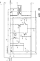
2 ist ein Schaltbild einer Ausführungsform einer in einen Verstärker integrierten IC oder IC 40. Die IC 40 beinhaltet den Stromniedrigversorgungsspannungspol 5, den Signalpol 6, den Stromhochversorgungsspannungspol 7, einen Verstärker 14, einen ersten Gleichrichter 15, einen zweiten Gleichrichter 16, eine Fehlerschutzschaltung 18 und eine Fehlerschutzsteuerschaltung 19. 2 FIG. 12 is a circuit diagram of one embodiment of an amplifier-integrated IC or IC. FIG 40 , The IC 40 includes the power low supply voltage pole 5 , the signal pole 6 , the high voltage power pole 7 , an amplifier 14 , a first rectifier 15 , a second rectifier 16 , an error protection circuit 18 and an error protection control circuit 19 ,
Die Fehlerschutzschaltung 18 beinhaltet einen ersten Fehlerschutz-PMOS-Transistor 27 und einen zweiten Fehlerschutz-PMOS-Transistor 28. Der erste Fehlerschutz-PMOS-Transistor 27 beinhaltet einen Drain, der elektrisch mit dem Ausgang des Verstärkers 14 verbunden ist. Der erste Fehlerschutz-PMOS-Transistor 27 beinhaltet ferner einen Körper und eine Quelle, die elektrisch mit einem Körper und einer Quelle des zweiten Fehlerschutz-PMOS-Transistors 28 und mit einem ersten Eingang des Fehlerschutzsteuerblocks 19 an einem Knoten N1 verbunden sind. Der erste Fehlerschutz-PMOS-Transistor 27 beinhaltet ferner ein Gate, das elektrisch mit dem ersten Ausgang des Fehlerschutzsteuerblocks 18 verbunden ist. Der zweite Fehlerschutz-PMOS-Transistor 28 beinhaltet ferner einen Drain, der elektrisch mit dem Signalpol 6 und einem zweiten Eingang des Fehlerschutzsteuerblocks 19 verbunden ist. Der zweite Fehlerschutz-PMOS-Transistor 28 beinhaltet ferner ein Gate, das elektrisch mit einem zweiten Ausgang des Fehlerschutzsteuerblocks 19 verbunden ist. Wie sie hierin verwendet werden und wie für Fachleute ersichtlich ist, können MOS-Transistoren Gates aufweisen, die aus nicht-metallischen Materialien, wie Polysilizium, hergestellt sind und in welche dielektrische Bereiche nicht nur mit Siliziumoxid sondern mit anderen Dielektrika, wie High-k-Dielektrika, implementiert sind.The error protection circuit 18 includes a first fault protection PMOS transistor 27 and a second fault protection PMOS transistor 28 , The first fault protection PMOS transistor 27 includes a drain electrically connected to the output of the amplifier 14 connected is. The first fault protection PMOS transistor 27 further includes a body and a source electrically connected to a body and a source of the second fault protection PMOS transistor 28 and a first input of the error protection control block 19 are connected at a node N 1 . The first fault protection PMOS transistor 27 further includes a gate electrically connected to the first output of the error protection control block 18 connected is. The second fault protection PMOS transistor 28 further includes a drain electrically connected to the signal pole 6 and a second input of the error protection control block 19 connected is. The second fault protection PMOS transistor 28 further includes a gate electrically connected to a second output of the error protection control block 19 connected is. As used herein, and as will be appreciated by those skilled in the art, MOS transistors may include gates made of non-metallic materials, such as polysilicon, and into which dielectric regions not only with silicon oxide but with other dielectrics, such as high-k Dielectrics are implemented.
Der Verstärker 14 beinhaltet einen Antriebs-NMOS-Transistor 21, einen Antriebs-PMOS-Transistor 22 und einen Ausgangsantriebssteuerblock 25. Der Antriebs-NMOS-Transistor 21 beinhaltet eine Quelle und einen Körper, die elektrisch mit dem Stromniedrigversorgungsspannungspol 5 verbunden sind, und ein Gate, das elektrisch mit einem ersten Ausgang des Ausgangsantriebssteuerblocks 25 verbunden ist. Der Antriebs-PMOS-Transistor 22 beinhaltet eine Quelle und einen Körper, die elektrisch mit dem Stromhochversorgungsspannungspol 7 verbunden sind, und ein Gate, das elektrisch mit einem zweiten Ausgang des Ausgangsantriebssteuerblocks 25 verbunden ist. Der Antriebs-NMOS-Transistor 21 beinhaltet ferner einen Drain, der an einem Ausgang des Verstärkers 14 elektrisch mit einem Drain des Antriebs-PMOS-Transistors 22 verbunden ist. Der Ausgang des Verstärkers 14 ist durch die Fehlerschutzschaltung 18 elektrisch mit dem Signalpol 6 verbunden. Wie in 2 dargestellt, kann der Verstärker 14 eine erste parasitäre Diode 23, die mit einer Drain-Körper-Anschlussstelle des Antriebs-NMOS-Transistors 21 verknüpft ist, und eine zweite parasitäre Diode 24, die mit einer Drain-Körper-Anschlussstelle des Antriebs-PMOS-Transistors 22 verknüpft ist, beinhalten.The amplifier 14 includes a drive NMOS transistor 21 , a drive PMOS transistor 22 and an output drive control block 25 , The drive NMOS transistor 21 includes a source and a body electrically connected to the low power supply voltage pole 5 and a gate electrically connected to a first output of the output drive control block 25 connected is. The drive PMOS transistor 22 includes a source and a body electrically connected to the power supply high voltage pole 7 and a gate electrically connected to a second output of the output drive control block 25 connected is. The drive NMOS transistor 21 further includes a drain connected to an output of the amplifier 14 electrically connected to a drain of the drive PMOS transistor 22 connected is. The output of the amplifier 14 is through the error protection circuit 18 electrically with the signal pole 6 connected. As in 2 shown, the amplifier can 14 a first parasitic diode 23 connected to a drain-body junction of the drive NMOS transistor 21 is linked, and a second parasitic diode 24 connected to a drain-body junction of the drive PMOS transistor 22 is linked include.
Der Verstärker 14 kann verwendet werden, um einen Spannungspegel des Signalpols 6 zu steuern. Wenn zum Beispiel der erste und zweite Fehlerschutz-PMOS-Transistor 27, 28 von der Fehlerschutzsteuerschaltung 19 eingeschaltet werden, kann der Verstärker 14 einen Spannungspegel des Signalpols 6 steuern, indem er unter Verwendung des Ausgangsantriebssteuerblocks 25 anhand des Antriebs-PMOS-Transistors 22 Stromstärke bezieht und/oder die Stromstärke anhand des Antriebs-NMOS-Transistors 21 senkt. Der erste und zweite Fehlerschutz-PMOS-Transistor 27, 28 sollten eine ausreichende Größe aufweisen, um einen relativ geringen AN-Zustand-RDS aufzuweisen, sodass die Spannungsaussteuerungsreserve nicht maßgeblich beeinflusst wird, wenn der Verstärker 14 Stromstärke zu oder von der Signalkontaktstelle 6 senkt oder bezieht.The amplifier 14 can be used to set a voltage level of the signal pole 6 to control. For example, if the first and second fault protection PMOS transistor 27 . 28 from the error protection control circuit 19 can be turned on, the amplifier 14 a voltage level of the signal pole 6 control by using the output drive control block 25 based on the drive PMOS transistor 22 Amperage refers and / or the current based on the drive NMOS transistor 21 lowers. The first and second fault protection PMOS transistor 27 . 28 should be of sufficient magnitude to have a relatively low ON state R DS so that the voltage headroom is not significantly affected when the amplifier 14 Amperage to or from the signal contact point 6 lower or lower.
Die erste und zweite bidirektionale Blockierungsklemme 15, 16 können verwendet werden, um eine Spannungsschwankung der Signalkontaktstelle 6 zu begrenzen. Die erste bidirektionale Blockierungsklemme 15 beinhaltet eine erste Blockierungsanschlussstelle 33 und eine zweite Blockierungsanschlussstelle 34. Die erste Blockierungsanschlussstelle 33 beinhaltet eine Anode, die elektrisch mit dem Stromniedrigversorgungsspannungspol 5 verbunden ist, und eine Kathode, die elektrisch mit einer Kathode der zweiten Blockierungsanschlussstelle 34 verbunden ist. Die zweite Blockierungsanschlussstelle 34 beinhaltet ferner eine Anode, die elektrisch mit dem Signalpol 6 verbunden ist. Die zweite bidirektionale Blockierungsklemme 16 beinhaltet eine dritte Blockierungsanschlussstelle 35 und eine vierte Blockierungsanschlussstelle 36. Die dritte Blockierungsanschlussstelle 35 beinhaltet eine Anode, die elektrisch mit dem Signalpol 6 verbunden ist, und eine Kathode, die elektrisch mit einer Kathode der vierten Blockierungsanschlussstelle 36 verbunden ist. Die vierte Blockierungsanschlussstelle 36 beinhaltet ferner eine Anode, die elektrisch mit dem Stromhochversorgungsspannungspol 7 verbunden ist.The first and second bidirectional blocking clamp 15 . 16 can be used to provide a voltage swing of the signal pad 6 to limit. The first bi-directional blocking clamp 15 includes a first blocking port 33 and a second blocking port 34 , The first blocking connection point 33 includes an anode electrically connected to the low power supply voltage pole 5 and a cathode electrically connected to a cathode of the second blocking junction 34 connected is. The second blocking connection point 34 further includes an anode electrically connected to the signal pole 6 connected is. The second bidirectional blocking clamp 16 includes a third blocking port 35 and a fourth blocking port 36 , The third blocking connection point 35 includes an anode that is electrically with the signal pole 6 and a cathode electrically connected to a cathode of the fourth blocking junction 36 connected is. The fourth blocking port 36 further includes an anode electrically connected to the power high voltage post 7 connected is.
Die Fehlerschutzsteuerschaltung 19 kann verwendet werden, um einen Zustand der Fehlerschutzschaltung 18 zu steuern, um den Ausgang des Verstärkers 14 vor Überspannungs- und Unterspannungsbedingungen auf der Signalkontaktstelle 6 zu schützen. Zum Beispiel kann das Abschalten des ersten und/oder zweiten Fehlerschutz-PMOS-Transistors 27, 28 während einer Überspannungs- oder Unterspannungsbedingung auf dem Signalpol 6 helfen, einen hohen Widerstand zwischen dem Ausgang des Verstärkers 14 und dem Signalpol 6 bereitzustellen. Da Überspannungs- und/oder Unterspannungsbedingungen auf dem Ausgang des Verstärkers 14 zu mit der Beaufschlagung der ersten und/oder zweiten parasitären Diode 23, 24 des Verstärkers 14 mit einer Vorwärtsspannung verknüpften Schäden führen können, kann die Fehlerschutzsteuerschaltung 19 verwendet werden, um den Verstärker 14 vor mit den Fehlerbedingungen auf dem Signalpol 6 verknüpften Schäden zu schützen. Während des normalen Betriebs des Verstärkers 14 kann die Fehlerschutzsteuerschaltung 19 konfiguriert sein, um den ersten und zweiten Fehlerschutz-PMOS-Transistor 18, 19 einzuschalten, sodass der Verstärker 14 einen Spannungspegel des Signalpols 6 steuern kann.The error protection control circuit 19 can be used to set a state of the error protection circuit 18 to control the output of the amplifier 14 against overvoltage and undervoltage conditions on the signal contact point 6 to protect. For example, turning off the first and / or second fault protection PMOS transistor 27 . 28 during an overvoltage or undervoltage condition on the signal pole 6 help, a high resistance between the output of the amplifier 14 and the signal pole 6 provide. Since overvoltage and / or undervoltage conditions on the output of the amplifier 14 to with the application of the first and / or second parasitic diode 23 . 24 of the amplifier 14 can lead to damage associated with a forward voltage, the error protection control circuit 19 used to the amplifier 14 before with the error conditions on the signal pole 6 protect associated damage. During normal operation of the amplifier 14 can the error protection control circuit 19 be configured to the first and second fault protection PMOS transistor 18 . 19 turn on, so the amplifier 14 a voltage level of the signal pole 6 can control.
Während einer Überspannungsbedingung auf dem Signalpol 6 kann die Fehlerschutzsteuerschaltung 19 konfiguriert sein, um den zweiten Fehlerschutz-PMOS-Transistor 28 einzuschalten oder eingeschaltet zu lassen und den ersten Fehlerschutz-PMOS-Transistor 27 abzuschalten. Das derartige Steuern des ersten und zweiten Fehlerschutz-PMOS-Transistors 27, 28 während einer Überspannungsbedingung kann verhindern, dass die Überspannungsbedingung den Verstärker 14 beschädigt, indem die Spannung über und Stromstärke durch den Antriebs-NMOS-Transistor 21 und den Antriebs-PMOS-Transistor 22 eingeschränkt wird. Zusätzlich ermöglicht es das Einschalten des zweiten Fehlerschutz-PMOS-Transistors 28 während der Überspannungsbedingung, dass der Spannungspegel der Körper des ersten und zweiten Fehlerschutz-PMOS-Transistors 27, 28 relativ nah an einem Spannungspegel des Signalpols 6 liegt, was dabei hilft, zu verhindern, dass parasitäre Drain-Körper-Dioden des ersten und zweiten Fehlerschutz-PMOS-Transistors 27, 28 während der Überspannungsbedingung mit einer Vorwärtsspannung beaufschlagt werden. Zum Beispiel kann die Konfigurierung der Fehlerschutzschaltung 18 auf diese Weise eine verbesserte Leistung im Verhältnis zu einem System bereitstellen, in dem der zweite Fehlerschutz-PMOS-Transistor 28 während einer Überspannungsbedingung abgeschaltet ist, was dazu führen kann, dass die parasitäre Drain-Körper-Diode des zweiten Fehlerschutz-PMOS-Transistors 28 währen der Überspannungsbedingung aktiviert wird.During an overvoltage condition on the signal pole 6 can the error protection control circuit 19 be configured to the second fault protection PMOS transistor 28 turn on or leave on and the first fault protection PMOS transistor 27 off. Such controlling the first and second fault protection PMOS transistor 27 . 28 during an overvoltage condition, the overvoltage condition can prevent the amplifier 14 Damaged by the voltage across and amperage through the drive NMOS transistor 21 and the drive PMOS transistor 22 is restricted. In addition, it enables the second fault protection PMOS transistor to be turned on 28 during the overvoltage condition, that the voltage level of the bodies of the first and second fault protection PMOS transistor 27 . 28 relatively close to a voltage level of the signal pole 6 which helps to prevent parasitic drain-body diodes of the first and second PMOS fault transistors 27 . 28 during the overvoltage condition, a forward voltage is applied. For example, the configuration of the error protection circuit 18 in this way provide improved performance relative to a system in which the second PMOS error protection transistor 28 is turned off during an overvoltage condition, which may cause the parasitic drain body diode of the second PMOS error protection transistor 28 during the overvoltage condition is activated.
Während einer Unterspannungsbedingung auf dem Signalpol 6 kann die Fehlerschutzsteuerschaltung 19 den ersten Fehlerschutz-PMOS-Transistor 27 einschalten oder eingeschaltet lassen und den zweiten Fehlerschutz-PMOS-Transistor 28 abschalten, was helfen kann, den Verstärker 14 vor übermäßigen Spannungs- und/oder übermäßigen Stromstärkenbedingungen zu schützen, und helfen kann, mit dem ersten und zweiten Fehlerschutz-PMOS-Transistor 27, 28 verknüpfte parasitäre Dioden am Aktivieren zu hindern. Zum Beispiel kann der Verstärker 14 durch Abschalten des zweiten Fehlerschutz-PMOS-Transistors 28 und durch Einschalten des ersten Fehlerschutz-PMOS-Transistors 27 während einer Unterspannungsbedingung auf dem Signalpol 6 ein elektrisches Potential der Körper des ersten und zweiten Fehlerschutz-PMOS-Transistors 27, 28 während der Unterspannungsbedingung steuern. Da der Spannungspegel des Signalpols 6 während einer Unterspannungsbedingung verhältnismäßig gering sein kann, kann die derartige Konfigurierung des ersten und zweiten Fehlerschutz-PMOS-Transistors 27, 28 verhindern, dass parasitäre Drain-Körper-Dioden des ersten und zweiten Fehlerschutz-PMOS-Transistors 27, 28 während der Unterspannungsbedingung aktiviert werden. Zum Beispiel kann die Konfigurierung des Fehlerschutzsteuerblocks 19, sodass sie den zweiten Fehlerschutz-PMOS-Transistor 28 während einer Unterspannungsbedingung abschaltet und den ersten Fehlerschutz-PMOS-Transistor 27 einschaltet, im Verhältnis zu einem System, in dem sowohl der erste als auch der zweite Fehlerschutz-PMOS-Transistor 27, 28 während der Unterspannungsbedingung abgeschaltet werden, was dazu führen kann, dass die parasitäre Drain-Körper-Diode des ersten Fehlerschutz-PMOS-Transistors 27 während der Unterspannungsbedingung aktiviert wird, eine verbesserte Leistung bereitstellen.During an undervoltage condition on the signal pole 6 can the error protection control circuit 19 the first fault protection PMOS transistor 27 turn on or leave on and the second fault protection PMOS transistor 28 turn off what can help the amplifier 14 to protect against excessive voltage and / or excessive current conditions, and can help with the first and second fault protection PMOS transistor 27 . 28 to prevent linked parasitic diodes from activating. For example, the amplifier 14 by turning off the second fault protection PMOS transistor 28 and by turning on the first fault protection PMOS transistor 27 during an undervoltage condition on the signal pole 6 an electrical potential of the bodies of the first and second fault protection PMOS transistor 27 . 28 during the undervoltage condition. As the voltage level of the signal pole 6 may be relatively low during an undervoltage condition, such configuration of the first and second PMOS error transistors 27 . 28 prevent parasitic drain body diodes of the first and second fault protection PMOS transistor 27 . 28 be activated during the undervoltage condition. For example, the configuration of the error protection control block 19 so that they have the second fault protection PMOS transistor 28 during an undervoltage condition turns off and the first fault protection PMOS transistor 27 turns on, in relation to a system in which both the first and the second fault protection PMOS transistor 27 . 28 be turned off during the undervoltage condition, which may cause the parasitic drain body diode of the first fault protection PMOS transistor 27 while the undervoltage condition is activated, provide improved performance.
In einer Ausführungsform beinhaltet die Fehlerschutzsteuerschaltung 19 eine Überspannungserkennungs- und -steuerschaltung 31 und eine Unterspannungserkennungs- und -steuerschaltung 32. Während des normalen Betriebs ist die Überspannungserkennungs- und -steuerschaltung 31 konfiguriert, um den ersten Fehlerschutz-PMOS-Transistor 27 einzuschalten und die Unterspannungserkennungs- und -steuerschaltung 32 ist konfiguriert, um den zweiten Fehlerschutz-PMOS-Transistor 28 einzuschalten. Zusätzlich ist die Überspannungserkennungs- und -steuerschaltung 31 konfiguriert, um eine Überspannungsbedingung zu erkennen, die mit dem Umstand verknüpft ist, dass ein Spannungspegel des Signalpols 6 einen Spannungspegel des Stromhochversorgungsspannungspols 7 um einen ersten Grenzwert übersteigt, und den ersten Fehlerschutz-PMOS-Transistor 27 abzuschalten, wenn die Überspannungsbedingung erkannt wird. Des Weiteren ist die Unterspannungserkennungs- und -steuerschaltung 32 konfiguriert, um eine Unterspannungsbedingung zu erkennen, die mit dem Umstand verknüpft ist, dass der Spannungspegel des Signalpols 6 um eine zweite Grenzwertspannung unter einen Spannungspegel des Stromniedrigversorgungsspannungspols 7 fällt, und den zweiten Fehlerschutz-PMOS-Transistor 28 abzuschalten, wenn die Unterspannungsbedingung erkannt wird. In einer Ausführungsform wird die erste Grenzwertspannung so ausgewählt, dass sie in den Bereich von ungefähr 1 V bis ungefähr 2 V fällt, und die zweite Grenzwertspannung wird so ausgewählt, dass sie in den Bereich von ungefähr 1 V bis ungefähr 2 V fällt.In one embodiment, the error protection control circuit includes 19 an overvoltage detection and control circuit 31 and a low voltage detection and control circuit 32 , During normal operation, the over-voltage detection and control circuit is 31 configured to the first fault protection PMOS transistor 27 and the undervoltage detection and control circuit 32 is configured to the second fault protection PMOS transistor 28 turn. In addition, the overvoltage detection and control circuit is 31 configured to detect an overvoltage condition associated with the circumstance that a voltage level of the signal pole 6 a voltage level of Stromhochversorgungsspannungspols 7 exceeds a first threshold, and the first fault protection PMOS transistor 27 switch off when the overvoltage condition is detected. Furthermore, the undervoltage detection and control circuit is 32 configured to detect an undervoltage condition associated with the fact that the voltage level of the signal pole 6 by a second threshold voltage below a voltage level of the low power supply voltage pole 7 falls, and the second fault protection PMOS transistor 28 switch off when the undervoltage condition is detected. In one embodiment, the first threshold voltage is selected to fall in the range of about 1 V to about 2 V, and the second threshold voltage is selected to fall within the range of about 1 V to about 2 V.
Die in 2 dargestellte Fehlerschutzschaltung 18 beinhaltet PMOS-Transistoren statt NMOS-Transistoren. Wenngleich alternativ NMOS-Transistoren verwendet werden können, wie später in Zusammenhang mit 7 beschrieben, kann die Verwendung von PMOS-Transistoren im Vergleich zu bestimmten Systemen, die NMOS-Transistoren verwenden, eine verbesserte Leistung bereitstellen, da NMOS-Transistoren parasitäre Drain-Substrat-Dioden beinhalten können, die aktiviert oder mit einer Vorwärtsspannung beaufschlagt werden können, wenn der Spannungspegel des Signalpols 6 unter den Spannungspegel des Stromniedrigversorgungsspannungspols V1 fällt. Wenngleich der erste und zweite PMOS-Transistor 27, 28 parasitäre Drain-Körper-Dioden beinhalten können, wie oben beschrieben wurde, kann die Fehlerschutzsteuerschaltung 19 den Spannungspegel der Gates des ersten und zweiten PMOS-Transistors 27, 28 während Überspannungs- und Unterspannungsbedingungen auf dem Signalpol 6 steuern, um zu verhindern, dass parasitäre Drain-Körper-Dioden mit einer Vorwärtsspannung beaufschlagt werden.In the 2 illustrated error protection circuit 18 includes PMOS transistors instead of NMOS transistors. Although, alternatively, NMOS transistors may be used as discussed later in connection with FIG 7 As described, the use of PMOS transistors may provide improved performance as compared to certain systems using NMOS transistors, as NMOS transistors may include parasitic drain-substrate diodes that may be activated or forward biased when the voltage level of the signal pole 6 falls below the voltage level of the low power supply voltage pole V 1 . Although the first and second PMOS transistor 27 . 28 parasitic drain body diodes, as described above, the error protection control circuit 19 the voltage level of the gates of the first and second PMOS transistors 27 . 28 during overvoltage and undervoltage conditions on the signal pole 6 to prevent parasitic drain body diodes from being supplied with a forward voltage.
In einer Ausführungsform sind der erste und zweite Fehlerschutz-PMOS-Transistor 27, 28 lateral diffuse P-Kanal-Metalloxid-Halbleiter-(LDMOS)-Geräte. Die Konfigurierung des ersten und zweiten PMOS-Transistors als LDMOS-Gerät kann dabei helfen, eine Maximalspannung zu erhöhen, welcher der erste und zweite PMOS-Transistor während einer Fehlerbedingung widerstehen können.In one embodiment, the first and second error protection PMOS transistors 27 . 28 laterally diffused P-channel metal oxide semiconductor (LDMOS) devices. The configuration of the first and second PMOS transistors as LDMOS devices may help increase a maximum voltage that the first and second PMOS transistors can withstand during a fault condition.
3A ist ein Schaltbild einer in einen Verstärker integrierten Schaltung IC oder IC 60, die eine Ausführungsform einer Überspannungserkennungs- und -steuerschaltung beinhaltet. Die IC 60 beinhaltet den Verstärker 4, den Stromniedrigversorgungsspannungspol 5, den Signalpol 6, den Stromhochversorgungsspannungspol 7 und die Fehlerschutzschaltung 18, die wie oben mit Verweis auf 1 und 2 beschrieben ausgeführt sein können. Ferner beinhaltet die IC 60 eine Fehlerschutzsteuerschaltung, die eine Überspannungserkennungs- und -steuerschaltung 41 und eine Unterspannungserkennungs- und -steuerschaltung 32 beinhaltet. 3A is a circuit diagram of an integrated circuit in an amplifier IC or IC 60 , which includes an embodiment of an overvoltage detection and control circuit. The IC 60 includes the amplifier 4 , the low power supply voltage pole 5 , the signal pole 6 , the high voltage power pole 7 and the error protection circuit 18 as referenced above 1 and 2 can be described described. Furthermore, the IC includes 60 an error protection control circuit including an overvoltage detection and control circuit 41 and a low voltage detection and control circuit 32 includes.
Die Überspannungserkennungs- und -steuerschaltung 41 beinhaltet eine Hochspannungsstromquelle 42, erste bis sechste Widerstände 43–48, einen ersten und zweiten NMOS-Transistor 51, 52 und erste bis vierte PMOS-Transistoren 53–56. Wie sie hierin verwendet wird, kann sich „Hochspannung” zum Beispiel auf Transistoren oder andere Schaltungen beziehen, die konfiguriert sind, um Spannungen im Bereich von ungefähr 20 V bis ungefähr 100 V, zum Beispiel 40 V, zu widerstehen, während sich „Niedrigspannung” auf Transistoren oder andere Schaltungen beziehen kann, die konfiguriert sind, um Spannungen im Bereich von ungefähr 1 V bis ungefähr 6 V, zum Beispiel 5 V, zu widerstehen. Die Hochspannungsstromquelle 42 beinhaltet eine erste Klemme, die elektrisch mit einer dritten Spannungsversorgung V3 verbunden ist, und eine zweite Klemme, die elektrisch mit einem Gate des ersten Fehlerschutz-PMOS-Transistors 27, mit einem ersten Ende des sechsten Widerstands 48 und mit einem Drain des ersten PMOS-Transistors 53 verbunden ist. Der sechste Widerstand 48 beinhaltet ferner ein zweites Ende, das elektrisch mit dem Knoten N1 der Fehlerschutzschaltung 18 verbunden ist. Der erste PMOS-Transistor 53 beinhaltet ferner eine Quelle, die elektrisch mit dem Knoten N1 verbunden ist, und ein Gate, das elektrisch mit einem Drain des dritten PMOS-Transistors 55, mit einem Gate und einem Drain des zweiten PMOS-Transistors 54 und mit einem Drain des zweiten NMOS-Transistors 52 verbunden ist. Der zweite PMOS-Transistor 54 beinhaltet ferner eine Quelle, die elektrisch mit dem Knoten N1 verbunden ist. Der dritte PMOS-Transistor 55 beinhaltet ferner eine Quelle, die elektrisch mit dem Knoten N1 verbunden ist, und ein Gate, das elektrisch mit einem Gate und mit einem Drain des vierten PMOS-Transistors 56 und mit einem Drain des ersten NMOS-Transistors 51 verbunden ist. Der vierte PMOS-Transistor 56 beinhaltet ferner eine Quelle, die elektrisch mit dem Knoten N1 verbunden ist.The overvoltage detection and control circuit 41 includes a high voltage power source 42 , first to sixth resistances 43 - 48 , a first and second NMOS transistor 51 . 52 and first to fourth PMOS transistors 53 - 56 , As used herein, "high voltage" may refer, for example, to transistors or other circuits configured to withstand voltages in the range of about 20V to about 100V, for example, 40V, while "low voltage" may refer to transistors or other circuits configured to withstand voltages in the range of about 1V to about 6V, for example, 5V. The high voltage power source 42 includes a first terminal electrically connected to a third voltage supply V 3 and a second terminal electrically connected to a gate of the first fault protection PMOS transistor 27 , with a first end of the sixth resistance 48 and a drain of the first PMOS transistor 53 connected is. The sixth resistance 48 further includes a second end electrically connected to the node N 1 of the fault protection circuit 18 connected is. The first PMOS transistor 53 Also includes a source electrically connected to node N 1 and a gate electrically connected to a drain of the third PMOS transistor 55 with a gate and a drain of the second PMOS transistor 54 and a drain of the second NMOS transistor 52 connected is. The second PMOS transistor 54 further includes a source electrically connected to node N 1 . The third PMOS transistor 55 Also includes a source electrically connected to node N 1 and a gate electrically connected to a gate and to a drain of the fourth PMOS transistor 56 and a drain of the first NMOS transistor 51 connected is. The fourth PMOS transistor 56 further includes a source electrically connected to node N 1 .
Der erste NMOS-Transistor 51 beinhaltet ferner ein Gate, das elektrisch mit einem ersten Ende des ersten Widerstands 43 und mit einem ersten Ende des zweiten Widerstands 44 verbunden ist. Der erste NMOS-Transistor 51 beinhaltet ferner eine Quelle, die elektrisch mit einer Quelle des zweiten NMOS-Transistors 52 und mit einem ersten Ende des fünften Widerstands 47 verbunden ist. Der zweite Widerstand 44 beinhaltet ferner ein zweites Ende, das elektrisch mit einer Referenzspannung VREF verbunden ist, die vom Stromhochversorgungsspannungspol 7 abgeleitet werden kann. Der zweite Widerstand 43 beinhaltet ferner ein zweites Ende, das elektrisch mit dem Stromniedrigversorgungsspannungspol 5 verbunden ist. Der fünfte Widerstand 47 beinhaltet ferner ein zweites Ende, das elektrisch mit der dritten Versorgungsspannung V3 verbunden ist. Der zweite NMOS-Transistor 52 beinhaltet ferner ein Gate, das elektrisch mit einem ersten Ende des dritten Widerstands 45 und mit einem ersten Ende des vierten Widerstands 46 verbunden ist. Der dritte Widerstand 45 beinhaltet ferner ein zweites Ende, das elektrisch mit dem Stromniedrigversorgungsspannungspol 5 verbunden ist. Der vierte Widerstand 46 beinhaltet ferner ein zweites Ende, das elektrisch mit dem Knoten N1 verbunden ist.The first NMOS transistor 51 further includes a gate electrically connected to a first end of the first resistor 43 and with a first end of the second resistor 44 connected is. The first NMOS transistor 51 further includes a source electrically connected to a source of the second NMOS transistor 52 and with a first end of the fifth resistor 47 connected is. The second resistance 44 further includes a second end electrically connected to a reference voltage V REF from the high voltage power pole 7 can be derived. The second resistance 43 also includes a second one End electrically connected to the low power supply voltage pole 5 connected is. The fifth resistance 47 further includes a second end electrically connected to the third supply voltage V 3 . The second NMOS transistor 52 further includes a gate electrically connected to a first end of the third resistor 45 and with a first end of the fourth resistor 46 connected is. The third resistance 45 further includes a second end electrically connected to the low power supply voltage pole 5 connected is. The fourth resistance 46 further includes a second end electrically connected to the node N 1 .
Die Überspannungserkennungs- und -steuerschaltung 41 kann den ersten Fehlerschutz-PMOS-Transistor 27 aktivieren oder einschalten, wenn keine Überspannungsbedingung auf dem Signalpol 6 erkannt wird. Wenn jedoch eine Überspannungsbedingung erkannt wird, kann die Überspannungserkennungs- und -steuerschaltung 41 den ersten Fehlerschutz-PMOS-Transistor 27 abschalten, um zu verhindern, dass eine große Menge an Stromstärke aus dem Signalpol 6 in den Ausgang des Verstärkers 4 fließt.The overvoltage detection and control circuit 41 can be the first fault protection PMOS transistor 27 enable or switch on if there is no overvoltage condition on the signal pole 6 is recognized. However, if an overvoltage condition is detected, the overvoltage detection and control circuit may 41 the first fault protection PMOS transistor 27 turn off to prevent a large amount of current from the signal pole 6 in the output of the amplifier 4 flows.
Der erste und zweite NMOS-Transistor 51, 52 können verwendet werden, um eine erste unter Verwendung eines ersten Spannungsteilers, der den ersten und zweiten Widerstand 43, 44 beinhaltet, erzeugte Spannung mit einer zweiten unter Verwendung eines zweiten Spannungsteilers, der den dritten und vierten Widerstand 45, 46 beinhaltet, erzeugten Spannung zu vergleichen. Zum Beispiel können der erste und zweite Widerstand 43, 44 verwendet werden, um basierend auf einem Spannungspegel der Referenzspannung VREF die erste Spannung zu erzeugen und der dritte und vierte Widerstand 45, 46 können verwendet werden, um basierend auf einem Spannungspegel des Signalpols 6 die zweite Spannung zu erzeugen. Durch das Auswählen eines Spannungspegels der Referenzspannung VREF und der Widerstände des ersten bis vierten Widerstands 43–46, kann die Überspannungserkennungs- und -steuerschaltung 41 konfiguriert sein, um eine Überspannungsbedingung mit einer gewünschten Größenordnung zu erkennen, wie eine Spannung, die eine Nennbetriebsspannung des Signalpols 6 um ungefähr 1 V bis ungefähr 2 V überschreitet. Der fünfte Widerstand 47 kann einen Vorbeeinflussungsstrom (bias currrent) an den ersten und zweiten NMOS-Transistor 51, 52 bereitstellen und ein Widerstand des fünften Widerstands 47 kann ausgewählt werden, um eine gewünschte Vergleichsreaktionszeit des ersten und zweiten NMOS-Transistors 51, 52 zu erzielen.The first and second NMOS transistors 51 . 52 may be used to generate a first voltage divider using the first and second resistors 43 . 44 includes, generated voltage with a second using a second voltage divider, the third and fourth resistor 45 . 46 involves comparing generated voltage. For example, the first and second resistances 43 . 44 be used to generate the first voltage based on a voltage level of the reference voltage V REF and the third and fourth resistor 45 . 46 can be used based on a voltage level of the signal pole 6 to generate the second voltage. By selecting a voltage level of the reference voltage V REF and the resistances of the first to fourth resistors 43 - 46 , the overvoltage detection and control circuit can 41 configured to detect an overvoltage condition of a desired magnitude, such as a voltage representing a nominal operating voltage of the signal pole 6 exceeds about 1 V to about 2 V. The fifth resistance 47 may apply a bias currrent to the first and second NMOS transistors 51 . 52 provide and a resistance of the fifth resistor 47 can be selected to provide a desired comparison reaction time of the first and second NMOS transistors 51 . 52 to achieve.
In einer Ausführungsform sind die Widerstände des dritten und vierten Widerstands 45, 46 relativ hoch gewählt, wie als kombinierter Reihenwiderstand von mehr als 1 Mega-Ω. Die Konfigurierung der Widerstände des dritten und vierten Widerstands 45, 46 als relativ hoch kann dabei helfen, eine Leckstromstärkenvorgabe des Signalpols 6 zu erzielen, wie eine Leckstromstärkenvorgabe von weniger als ungefähr 10 μA, wenn der Signalpol 6 bei ungefähr 5 V liegt.In one embodiment, the resistances of the third and fourth resistors are 45 . 46 relatively high, as a combined series resistance of more than 1 Mega-Ω. The configuration of the resistors of the third and fourth resistor 45 . 46 Being relatively high can help in providing a leakage current setpoint of the signal pole 6 such as a leakage current setpoint of less than about 10 μA when the signal pole 6 is about 5V.
Wenn eine Überspannungsbedingung auf dem Signalpol 6 erkannt wird, kann eine Stromstärke durch den zweiten NMOS-Transistor 52 eine Stromstärke durch den ersten NMOS-Transistor 51 übersteigen und der zweite NMOS-Transistor 52 kann den ersten und zweiten PMOS-Transistor 53, 54 verwenden, um die Gate-Spannung des ersten Fehlerschutz-PMOS-Transistors 27 so hochzuziehen, dass der erste Fehlerschutz-PMOS-Transistor 27 abgeschaltet wird. Wenn jedoch keine Überspannungsbedingung erkannt wird, kann die Stromstärke durch den ersten NMOS-Transistor 51 die Stromstärke durch den zweiten NMOS-Transistor 52 übersteigen und der erste NMOS-Transistor 51 kann den dritten und vierten PMOS-Transistor 55, 56 verwenden, um den ersten und zweiten PMOS-Transistor 53, 54 abzuschalten, was dazu führen kann, dass die Hochspannungsstromquelle 42 die Gate-Spannung des ersten Fehlerschutz-PMOS-Transistors 27 herunterzieht. Wenn zum Beispiel der erste und zweite PMOS-Transistor 53, 54 abgeschaltet werden, kann eine Stromstärke der Hochspannungsstromquelle 42 durch den sechsten Widerstand 48 fließen und die Gate-Quelle-Spannung des ersten Fehlerschutz-PMOS-Transistors 27 kann ungefähr dem Spannungsabfall über den sechsten Widerstand 48 entsprechen.When an overvoltage condition on the signal pole 6 is detected, a current through the second NMOS transistor 52 a current through the first NMOS transistor 51 exceed and the second NMOS transistor 52 may be the first and second PMOS transistor 53 . 54 use the gate voltage of the first fault protection PMOS transistor 27 pull it up so that the first fault protection PMOS transistor 27 is switched off. However, if no overvoltage condition is detected, the current through the first NMOS transistor 51 the current through the second NMOS transistor 52 exceed and the first NMOS transistor 51 can be the third and fourth PMOS transistor 55 . 56 use the first and second PMOS transistor 53 . 54 turn off, which can lead to the high voltage power source 42 the gate voltage of the first fault protection PMOS transistor 27 pulls down. For example, if the first and second PMOS transistors 53 . 54 can be turned off, a current of the high voltage power source 42 through the sixth resistance 48 and the gate-source voltage of the first fault protection PMOS transistor 27 can be about the voltage drop across the sixth resistor 48 correspond.
Das Einbeziehen des dritten und vierten PMOS-Transistors 55, 56 kann dabei helfen, die beständige Leckstromstärke zu minimieren, indem sichergestellt wird, dass der erste und zweite PMOS-Transistor 53, 54 während des normalen Betriebs abgeschaltet sind. In einer Ausführungsform ist der erste PMOS-Transistor 53 verhältnismäßig groß bemessen, um eine relativ schnelle Anstiegsrate für das Gate des ersten Fehlerschutz-PMOS-Transistors 27 während einer Überspannungsbedingung bereitzustellen.The inclusion of the third and fourth PMOS transistors 55 . 56 can help minimize the steady leakage current by ensuring that the first and second PMOS transistors 53 . 54 are switched off during normal operation. In an embodiment, the first PMOS transistor is 53 relatively large, at a relatively fast slew rate for the gate of the first fault protection PMOS transistor 27 during an overvoltage condition.
Während einer Überspannungsbedingung auf dem Signalpol 6 kann der zweite Fehlerschutz-PMOS-Transistor 28 durch den Unterspannungserkennungs- und -steuerblock 32 eingeschaltet werden. Das Einschalten des zweiten Fehlererkennungs-PMOS-Transistors 28 während einer Überspannungsbedingung auf dem Signalpol 6 kann verhindern, dass eine mit dem zweiten Fehlerschutz-PMOS-Transistor 28 verknüpfte parasitäre Drain-Körper-Diode während einer Überspannungsbedingung aktiviert wird.During an overvoltage condition on the signal pole 6 may be the second fault protection PMOS transistor 28 through the undervoltage detection and control block 32 be turned on. Turning on the second fault detection PMOS transistor 28 during an overvoltage condition on the signal pole 6 can prevent one with the second fault protection PMOS transistor 28 connected parasitic drain body diode is activated during an overvoltage condition.
In der in 3A gezeigten Konfigurierung wird die Überspannungserkennungs- und -steuerschaltung 41 unter Verwendung des Signalpols 6 vorgespannt oder mit Strom versorgt, wodurch die Überspannungserkennungs- und -steuerschaltung 41 sogar dann funktionieren kann, wenn der Stromhochversorgungsspannungspol 7 potentialfrei ist. Zusätzlich kann die Konfigurierung der Überspannungserkennungs- und -steuerschaltung 41 auf diese Weise dabei helfen, die Überspannungserkennungs- und -steuerschaltung 41 basierend auf einem Ausmaß der Überspannungsbedingung dynamisch vorzubeeinflussen (biasing). Wenn zum Beispiel der Spannungspegel des Signalpols 6 normale Betriebsbedingungen um ein relativ geringes Maß überschreitet, kann eine Stromstärke vom Signalpol 6, die über den zweiten Fehlerschutz-PMOS-Transistor 28 an die Überspannungserkennungs- und -steuerschaltung 41 bereitgestellt wird, relativ klein sein. Wenn der Spannungspegel des Signalpols 6 jedoch normale Betriebsbedingungen um ein relativ hohes Maß überschreitet, wie wenn ein gemäß ISO-7637-3 definiertes transientes Ereignis auf dem Signalpol 6 empfangen wird, kann die Überspannungserkennungs- und -steuerschaltung 41 mit einer relativ hohen Stromstärke vorgespannt sein und den ersten Fehlerschutz-PMOS-Transistor 27 relativ schnell abschalten. Da eine mit dem ersten Fehlerschutz-PMOS-Transistor 27 verknüpfte Gate-Kapazität relativ groß sein kann, kann das dynamische Anpassen der an die Überspannungserkennungs- und -steuerschaltung 41 bereitgestellten Stromstärke beim Senken des Stromverbrauchs helfen. In the in 3A The configuration shown becomes the overvoltage detection and control circuit 41 using the signal pole 6 biased or energized, whereby the overvoltage detection and control circuit 41 even when the power supply voltage pole can work 7 is potential-free. In addition, the configuration of the overvoltage detection and control circuit 41 help in this way, the overvoltage detection and control circuit 41 biasing based on an amount of overvoltage condition. If, for example, the voltage level of the signal pole 6 Normal operating conditions exceeds by a relatively small amount, a current from the Signalpol 6 connected via the second fault protection PMOS transistor 28 to the overvoltage detection and control circuit 41 is provided, be relatively small. When the voltage level of the signal pole 6 however, exceeds normal operating conditions by a relatively high level, such as when a transient event as defined in ISO-7637-3 occurs on the signal pole 6 is received, the overvoltage detection and control circuit 41 be biased with a relatively high current and the first fault protection PMOS transistor 27 switch off relatively quickly. As one with the first fault protection PMOS transistor 27 associated gate capacitance may be relatively large, the dynamic matching to the over-voltage detection and control circuit 41 provided power help reduce power consumption.
Die dritte Spannungsversorgung V3 kann als Stromniedrigversorgungsspannung für Komponenten der Überspannungs- und Unterspannungserkennungs- und -steuerschaltungen 41, 32 verwendet werden, die verwendet werden, um die Gate-Spannungen des ersten und zweiten Fehlerschutz-PMOS-Transistors 27, 28 zu steuern. Zum Beispiel wurde die dritte Spannungsversorgung V3 als eine Stromniedrigversorgungsspannung für die Hochspannungsstromquelle 42 verwendet, die verwendet wird, um eine Gate-Spannung des ersten Fehlerschutz-PMOS-Transistors 27 zu steuern, wenn auf dem Signalpol 6 keine Überspannungsbedingung erkannt wird. Der Spannungspegel der dritten Spannungsversorgung V3 kann so ausgewählt werden, dass er kleiner ist als der des Stromniedrigversorgungsspannungspols 5. Das derartige Konfigurieren der dritten Spannungsversorgung V3 kann die Ausgangsspannungsschwankung des Signalpols 6 erhöhen, indem die Gate-Spannungen des ersten und zweiten Fehlerschutz-PMOS-Transistors 27, 28 auf Spannungspegel gesteuert werden, die unter denen des Stromniedrigversorgungsspannungspols 5 liegen. Wenngleich 3A eine Konfigurierung mit der dritten Spannungsversorgung V3 zeigt, kann die dritte Spannungsversorgung V3 in bestimmten Ausführungen weggelassen werden, wie in Konfigurierungen, die eine verringerte Ausgangsspannungsschwankung auf dem Signalpol 6 aufweisen und/oder Konfigurierungen, in denen der erste und zweite Fehlerschutz-PMOS-Transistor 27, 28 Verarmungsmodus-MOS-Transistoren oder andere Feldeffekt-Transistoren (FETs) sind.The third power supply V 3 can be used as a power supply low voltage for components of the overvoltage and under voltage detection and control circuits 41 . 32 used, which are used to the gate voltages of the first and second fault protection PMOS transistor 27 . 28 to control. For example, the third power supply V 3 has become a low power supply voltage for the high voltage power source 42 which is used to provide a gate voltage of the first fault protection PMOS transistor 27 to steer when on the signal pole 6 no overvoltage condition is detected. The voltage level of the third power supply V 3 may be selected to be smaller than that of the power low power supply voltage pole 5 , The thus configuring the third power supply V 3 may change the output voltage fluctuation of the signal pole 6 increase, by the gate voltages of the first and second fault protection PMOS transistor 27 . 28 be controlled to voltage levels lower than those of the Stromnieg supply voltage pole 5 lie. Although 3A 3 shows a configuration with the third power supply V 3 , the third power supply V 3 may be omitted in certain embodiments, as in configurations that have a reduced output voltage swing on the signal pole 6 and / or configurations in which the first and second fault protection PMOS transistor 27 . 28 Depletion mode MOS transistors or other field effect transistors (FETs) are.
In der dargestellten Konfigurierung wird die dritte Spannungsversorgung V3 außerdem als eine Stromniedrigversorgungsspannung für den fünften Widerstand 47 verwendet. Der fünfte Widerstand 47 kann verwendet werden, um einen Vorbeeinflussungsstrom bereitzustellen, die sich sogar dann im Verhältnis zu einer Spannung des Signalpols 6 verändert, wenn die Stromversorgungspole falsch angeschlossen und/oder potentialfrei sind, wodurch die Fehlerbedingungserkennung verbessert wird. Wenn die Stromversorgungspole zum Beispiel falsch angeschlossen, potentialfrei oder eine Kombination davon sind, kann zum Beispiel ein Spannungspegel des Signalpols 6 über den Stromhochversorgungsspannungspol 7 steigen, und zu einer Überspannungsbedingung führen, die durch die Überspannungserkennungs- und -steuerschaltung 41 erkannt werden kann.In the illustrated configuration, the third voltage supply V 3 also becomes a current supply low voltage for the fifth resistor 47 used. The fifth resistance 47 can be used to provide a bias current even in relation to a voltage of the signal pole 6 changes if the power supply poles are incorrectly connected and / or floating, improving the fault condition detection. For example, if the power supply poles are incorrectly connected, floating, or a combination thereof, a voltage level of the signal pole may be 6 over the Stromhochversorgungsspannungspol 7 rise, and lead to an overvoltage condition caused by the overvoltage detection and control circuit 41 can be recognized.
3B ist ein Schaltbild einer in einen Verstärker integrierten Schaltung IC oder IC 80, die eine Ausführungsform einer Unterspannungserkennungs- und -steuerschaltung beinhaltet. Die IC 80 beinhaltet den Verstärker 4, den Stromniedrigversorgungsspannungspol 5, den Signalpol 6, den Stromhochversorgungsspannungspol 7 und die Fehlerschutzschaltung 18, die wie oben beschrieben ausgeführt sein können. Ferner beinhaltet die IC 80 eine Fehlerschutzsteuerschaltung, die eine Überspannungserkennungs- und -steuerschaltung 31 und eine Unterspannungserkennungs- und -steuerschaltung 62 beinhaltet. 3B is a circuit diagram of an integrated circuit in an amplifier IC or IC 80 , which includes an embodiment of a low voltage detection and control circuit. The IC 80 includes the amplifier 4 , the low power supply voltage pole 5 , the signal pole 6 , the high voltage power pole 7 and the error protection circuit 18 which may be implemented as described above. Furthermore, the IC includes 80 an error protection control circuit including an overvoltage detection and control circuit 31 and a low voltage detection and control circuit 62 includes.
Die Unterspannungserkennungs- und -steuerschaltung 62 beinhaltet eine Hochspannungsstromquelle 63, erste bis dritte Widerstände 64–66, einen ersten und zweiten NMOS-Transistor 71, 72 und erste bis vierte PMOS-Transistoren 73–76. Die Hochspannungsstromquelle 63 beinhaltet eine erste Klemme, die elektrisch mit einer dritten Spannungsversorgung V3 verbunden ist, und eine zweite Klemme, die elektrisch mit einem Gate des zweiten Fehlerschutz-PMOS-Transistors 28, mit einem ersten Ende des dritten Widerstands 66 und mit einem Drain des zweiten PMOS-Transistors 74 verbunden ist. Der dritte Widerstand 66 beinhaltet ferner ein zweites Ende, das elektrisch mit dem Knoten N1 der Fehlerschutzschaltung 18 verbunden ist. Der zweite PMOS-Transistor 74 beinhaltet ferner eine Quelle, die elektrisch mit dem Knoten N1 verbunden ist, und ein Gate, das elektrisch mit einem Drain des vierten PMOS-Transistors 76, mit einem Gate und einem Drain des dritten PMOS-Transistors 73 und mit einem Drain des ersten NMOS-Transistors 71 verbunden ist. Der erste PMOS-Transistor 73 beinhaltet ferner eine Quelle, die elektrisch mit dem Knoten N1 verbunden ist. Der vierte PMOS-Transistor 76 beinhaltet ferner eine Quelle, die elektrisch mit dem Knoten N1 verbunden ist, und ein Gate, das elektrisch mit einem Gate und mit einem Drain des dritten PMOS-Transistors 75 und mit einem Drain des zweiten NMOS-Transistors 72 verbunden ist. Der dritte PMOS-Transistor 75 beinhaltet ferner eine Quelle, die elektrisch mit dem Knoten N1 verbunden ist. Der erste NMOS-Transistor 71 beinhaltet ferner ein Gate, das elektrisch mit dem Stromniedrigversorgungsspannungspol 5 verbunden ist, und eine Quelle, die elektrisch mit einem ersten Ende des ersten Widerstands 64 und mit einer Quelle des zweiten NMOS-Transistors 72 verbunden ist. Der erste Widerstand 64 beinhaltet ferner ein zweites Ende, das elektrisch mit der dritten Versorgungsspannung V3 verbunden ist. Der zweite NMOS-Transistor 72 beinhaltet ferner ein Gate, das elektrisch mit einem ersten Ende des zweiten Widerstands 65 verbunden ist. Der zweite Widerstand 65 beinhaltet ferner ein zweites Ende, das elektrisch mit dem Signalpol 6 verbunden ist.The undervoltage detection and control circuit 62 includes a high voltage power source 63 , first to third resistances 64 - 66 , a first and second NMOS transistor 71 . 72 and first to fourth PMOS transistors 73 - 76 , The high voltage power source 63 includes a first terminal electrically connected to a third voltage supply V 3 and a second terminal electrically connected to a gate of the second fault protection PMOS transistor 28 , with a first end of the third resistor 66 and a drain of the second PMOS transistor 74 connected is. The third resistance 66 further includes a second end electrically connected to the node N 1 of the fault protection circuit 18 connected is. The second PMOS transistor 74 Also includes a source electrically connected to node N 1 and a gate electrically connected to a drain of the fourth PMOS transistor 76 , with a gate and a drain of the third PMOS transistor 73 and a drain of the first NMOS transistor 71 connected is. The first PMOS transistor 73 further includes a source electrically connected to node N 1 . The fourth PMOS transistor 76 Also includes a source electrically connected to node N 1 and a gate electrically connected to a gate and to a drain of the third PMOS transistor 75 and a drain of the second NMOS transistor 72 connected is. The third PMOS transistor 75 further includes a source electrically connected to node N 1 . The first NMOS transistor 71 further includes a gate electrically connected to the low power supply voltage pole 5 is connected, and a source electrically connected to a first end of the first resistor 64 and a source of the second NMOS transistor 72 connected is. The first resistance 64 further includes a second end electrically connected to the third supply voltage V 3 . The second NMOS transistor 72 further includes a gate electrically connected to a first end of the second resistor 65 connected is. The second resistance 65 further includes a second end electrically connected to the signal pole 6 connected is.
Die Unterspannungserkennungs- und -steuerschaltung 62 kann den zweiten Fehlerschutz-PMOS-Transistor 28 aktivieren oder einschalten, wenn keine Unterspannungsbedingung auf dem Signalpol 6 erkannt wird. Wenn jedoch eine Unterspannungsbedingung erkannt wird, kann die Unterspannungserkennungs- und -steuerschaltung 62 den zweiten Fehlerschutz-PMOS-Transistor 28 abschalten, um zu verhindern, dass eine große Menge an Stromstärke aus dem Signalpol 6 in den Ausgang des Verstärkers 4 fließt.The undervoltage detection and control circuit 62 can be the second fault protection PMOS transistor 28 activate or switch on if there is no undervoltage condition on the signal pole 6 is recognized. However, if an undervoltage condition is detected, the undervoltage detection and control circuit may 62 the second fault protection PMOS transistor 28 turn off to prevent a large amount of current from the signal pole 6 in the output of the amplifier 4 flows.
Der erste und zweite NMOS-Transistor 71, 72 können verwendet werden, um eine erste mit einem Spannungspegel des Stromniedrigversorgungsspannungspol 5 verknüpfte Spannung mit einer zweiten mit einem Spannungspegel des Signalpols 6 verknüpften Spannung zu vergleichen. In bestimmten Ausführungsformen ist der Unterspannungserkennungs- und -steuerblock 62 konfiguriert, um eine mit einer Spannung, die wenigstens ungefähr 1 V bis ungefähr 2 V unter einer Nennbetriebsspannung des Signalpols 6 liegt, verknüpfte Unterspannungsbedingung zu erkennen.The first and second NMOS transistors 71 . 72 may be used to connect a first to a voltage level of the low power supply voltage pole 5 linked voltage with a second with a voltage level of the signal pole 6 to compare linked voltage. In certain embodiments, the undervoltage detection and control block is 62 configured to be at a voltage that is at least about 1 V to about 2 V below a nominal operating voltage of the signal pole 6 lies to detect associated undervoltage condition.
Wenn die Unterspannungsbedingung erkannt wird, kann eine Stromstärke durch den ersten NMOS-Transistor 71 eine Stromstärke durch den zweiten NMOS-Transistor 72 übersteigen und der erste NMOS-Transistor 71 kann den ersten und zweiten PMOS-Transistor 73, 74 verwenden, um die Gate-Spannung des zweiten Fehlerschutz-PMOS-Transistors 28 so hochzuziehen, dass der zweite Fehlerschutz-PMOS-Transistor 28 abgeschaltet wird. Wenn jedoch keine Unterspannungsbedingung erkannt wird, kann die Stromstärke durch den zweiten NMOS-Transistor 72 die Stromstärke durch den ersten NMOS-Transistor 71 übersteigen und der zweite NMOS-Transistor 72 kann den dritten und vierten PMOS-Transistor 75, 76 verwenden, um den ersten und zweiten PMOS-Transistor 73, 74 abzuschalten, was dazu führen kann, dass die Hochspannungsstromquelle 63 die Gate-Spannung des zweiten Fehlerschutz-PMOS-Transistors 28 herunterzieht. Wenn zum Beispiel der erste und zweite PMOS-Transistor 73, 74 abgeschaltet werden, kann eine Stromstärke der Hochspannungsstromquelle 63 durch den dritten Widerstand 66 fließen und die Gate-Quelle-Spannung des zweiten Fehlerschutz-PMOS-Transistors 28 kann ungefähr dem Spannungsabfall über den dritten Widerstand 66 entsprechen.When the undervoltage condition is detected, a current through the first NMOS transistor 71 a current through the second NMOS transistor 72 exceed and the first NMOS transistor 71 may be the first and second PMOS transistor 73 . 74 use the gate voltage of the second fault protection PMOS transistor 28 pull it up so that the second fault protection PMOS transistor 28 is switched off. However, if no undervoltage condition is detected, the current through the second NMOS transistor 72 the current through the first NMOS transistor 71 exceed and the second NMOS transistor 72 can be the third and fourth PMOS transistor 75 . 76 use the first and second PMOS transistor 73 . 74 turn off, which can lead to the high voltage power source 63 the gate voltage of the second fault protection PMOS transistor 28 pulls down. For example, if the first and second PMOS transistors 73 . 74 can be turned off, a current of the high voltage power source 63 through the third resistance 66 and the gate-source voltage of the second fault protection PMOS transistor 28 can be about the voltage drop across the third resistor 66 correspond.
Während einer Unterspannungsbedingung auf dem Signalpol 6 kann der erste Fehlerschutz-PMOS-Transistor 27 durch den Überspannungserkennungs- und -steuerblock 31 eingeschaltet werden. Durch das Einschalten des ersten Fehlerschutz-PMOS-Transistors 27 während einer Unterspannungsbedingung auf dem Signalpol 6 kann vermieden werden, dass eine mit dem ersten Fehlerschutz-PMOS-Transistor 27 verknüpfte parasitäre Drain-Körper-Diode während einer Unterspannungsbedingung aktiviert wird.During an undervoltage condition on the signal pole 6 may be the first fault protection PMOS transistor 27 through the overvoltage detection and control block 31 be turned on. By turning on the first fault protection PMOS transistor 27 during an undervoltage condition on the signal pole 6 can be avoided that one with the first fault protection PMOS transistor 27 linked parasitic drain-body diode is activated during an undervoltage condition.
Wie in 3B gezeigt, kann die Unterspannungserkennungs- und -steuerschaltung 62 unter Verwendung des Signalpols 6 mit Strom versorgt werden, wodurch die Unterspannungserkennungs- und -steuerschaltung 62 sogar dann funktionieren kann, wenn die Stromversorgungspole falsch angeschlossen, potentialfrei oder eine Kombination davon sind. Zusätzlich kann die derartige Konfigurierung der Unterspannungserkennungs- und -steuerschaltung 62 dabei helfen, die Unterspannungserkennungs- und -steuerschaltung 62 als Reaktion auf eine Unterspannungsbedingung dynamisch vorzubeeinflussen. Zusätzliche Einzelheiten der Unterspannungserkennungs- und -steuerschaltung 62 aus 3B können den vorher mit Verweis auf die Überspannungserkennungs- und -steuerschaltung 41 aus 3A beschriebenen ähneln.As in 3B shown, the undervoltage detection and control circuit 62 using the signal pole 6 be energized, whereby the undervoltage detection and control circuit 62 even if the power supply poles are incorrectly connected, floating or a combination thereof. In addition, such configuration of the undervoltage detection and control circuit 62 help with the undervoltage detection and control circuit 62 to dynamically influence in response to an undervoltage condition. Additional details of the undervoltage detection and control circuit 62 out 3B may be previously with reference to the overvoltage detection and control circuit 41 out 3A similar to those described.
4A ist ein Schaltbild einer IC 100, die eine andere Ausführungsform einer Überspannungserkennungs- und -steuerschaltung beinhaltet. Die IC 100 beinhaltet den Verstärker 4, den Stromniedrigversorgungsspannungspol 5, den Signalpol 6, den Stromhochversorgungsspannungspol 7, die Fehlerschutzschaltung 18, den Unterspannungserkennungs- und -steuerblock 32, einen Überspannungserkennungs- und -steuerblock 81 und eine Ladungspumpe 82. 4A is a circuit diagram of an IC 100 , which includes another embodiment of an overvoltage detection and control circuit. The IC 100 includes the amplifier 4 , the low power supply voltage pole 5 , the signal pole 6 , the high voltage power pole 7 , the error protection circuit 18 , the undervoltage detection and control block 32 , an overvoltage detection and control block 81 and a charge pump 82 ,
Die IC 100 aus 4A ähnelt der IC 60 aus 3A, außer dass die IC 100 aus 4A ferner die Ladungspumpe 82 beinhaltet und eine andere Implementierung des Überspannungserkennungs- und -steuerblocks beinhaltet. The IC 100 out 4A resembles the IC 60 out 3A except that the IC 100 out 4A furthermore the charge pump 82 includes and includes another implementation of the overvoltage detection and control block.
Die Ladungspumpe 82 kann eine Negativladungspumpe sein, die konfiguriert ist, um eine Ladungspumpenversorgungsspannung VCP zu erzeugen, die einen Spannungspegel aufweist, der niedriger ist als ein Spannungspegel des Stromniedrigversorgungspannungspols 5. In bestimmten Ausführungsformen wird die Ladungspumpe 82 unter Verwendung der Stromhoch- und Stromniedrigversorgungsspannungspole 5, 6 mit Strom versorgt. Das Einbeziehen der Ladungspumpe 82 kann dabei helfen, die Ausgangsspannungsschwankung der Signalkontaktstelle 6 zu erhöhen, indem zugelassen wird, dass die Überspannungs- und Unterspannungserkennungs- und -steuerschaltungen 81, 32 die Spannungspegel der Gates des ersten und zweiten Fehlerschutz-PMOS-Transistors 27, 28 unter den Spannungspegel des Stromniedrigversorgungsspannungspols 5 steuern.The charge pump 82 may be a negative charge pump configured to generate a charge pump supply voltage V CP having a voltage level lower than a voltage level of the low current supply voltage pole 5 , In certain embodiments, the charge pump becomes 82 using the current high and low power supply voltage poles 5 . 6 powered. Including the charge pump 82 can help with the output voltage fluctuation of the signal pad 6 by allowing the overvoltage and undervoltage detection and control circuits to be increased 81 . 32 the voltage levels of the gates of the first and second fault protection PMOS transistor 27 . 28 below the voltage level of the low power supply voltage pole 5 Taxes.
Die Überspannungserkennungs- und -steuerschaltung 81 beinhaltet erste bis sechste Widerstände 43–48, einen ersten und zweiten NMOS-Transistor 51, 52 und erste bis vierte PMOS-Transistoren 53–56, die wie oben mit Verweis auf 3A beschrieben ausgeführt sein können. Die Überspannungserkennungs- und -steuerschaltung 81 beinhaltet ferner eine Hochspannungsstromquelle 83 und eine Einschwingverhalten-Verstärkungsschaltung 90. Die Überspannungserkennungs- und -steuerschaltung 81 ist unter Verwendung des Signalpols 6 vorbeeinflusst oder mit Energie versorgt, wodurch sogar dann Fehlerschutz bereitgestellt werden kann, wenn der Stromhochversorgungsspannungspol 7 und/oder der Stromniedrigversorgungsspannungspol 5 falsch angeschlossen, potentialfrei oder eine Kombination davon ist/sind. Zusätzlich wurde die Überspannungserkennungs- und -steuerschaltung 81 so konfiguriert, dass sie eine dynamische Vorbeeinflussung verwendet. Zum Beispiel basiert eine an die Überspannungserkennungs- und -steuerschaltung 81 bereitgestellte Stromstärke auf einer Größenordnung der Überspannungsbedingung. Wie unten ausführlicher beschrieben wird, kann eine dynamische Vorbeeinflussung durch die Verwendung der Einschwingverhalten-Verstärkungsschaltung 90 verstärkt werden.The overvoltage detection and control circuit 81 includes first to sixth resistances 43 - 48 , a first and second NMOS transistor 51 . 52 and first to fourth PMOS transistors 53 - 56 as referenced above 3A can be described described. The overvoltage detection and control circuit 81 further includes a high voltage power source 83 and a transient response amplification circuit 90 , The overvoltage detection and control circuit 81 is using the signal pole 6 Prevented or energized, whereby even then protection can be provided when the Stromhochversorgungsspannungspol 7 and / or the low power supply voltage pole 5 connected incorrectly, floating or a combination thereof is / are. In addition, the overvoltage detection and control circuit has become 81 configured to use dynamic bias. For example, one is based on the overvoltage detection and control circuit 81 provided current on an order of magnitude of the overvoltage condition. As will be described in more detail below, dynamic bias may be provided by the use of the transient gain amplifier circuit 90 be strengthened.
Die Hochspannungsstromquelle 83 beinhaltet eine Stromquelle 84, einen N-Kanal-LDMOS-(NLDMOS)-Transistor 85, eine Zenerdiode 86 und einen Stromquellensteuerblock 87. Der NLDMOS-Transistor 85 beinhaltet ein Gate, das elektrisch mit einer Vorbeeinflussungsspannung (bias voltage) VBIAS verbunden ist, und einen Körper und eine Quelle, die elektrisch mit einer ersten Klemme der Stromquelle 84 verbunden sind. Die Stromquelle 84 beinhaltet ferner eine zweite Klemme, die elektrisch mit der Ladungspumpenspannung VCP verbunden ist. Der NLDMOS-Transistor 85 beinhaltet ferner einen Drain, der elektrisch mit einem Gate des ersten Fehlerschutz-PMOS-Transistors 27 und mit einer Anode der Zenerdiode 86 verbunden ist. Zusätzlich beinhaltet der NLDMOS-Transistor 85 ferner einen N-Kanal-Isolationsbereich oder eine Wanne, der/die elektrisch mit einer Kathode der Zenerdiode 86 und mit einem Ausgang des Stromquellensteuerblocks 87 verbunden ist.The high voltage power source 83 includes a power source 84 , an N-channel LDMOS (NLDMOS) transistor 85 , a Zener diode 86 and a power source control block 87 , The NLDMOS transistor 85 includes a gate electrically connected to a bias voltage V BIAS , and a body and a source electrically connected to a first terminal of the power source 84 are connected. The power source 84 further includes a second terminal electrically connected to the charge pump voltage V CP . The NLDMOS transistor 85 further includes a drain electrically connected to a gate of the first fault protection PMOS transistor 27 and with an anode of the zener diode 86 connected is. In addition, the NLDMOS transistor includes 85 and an N-channel isolation region or well electrically connected to a cathode of the Zener diode 86 and with an output of the power source control block 87 connected is.
Die N-Kanal-Wanne des NLDMOS-Transistors 85 kann eine N-Kanal-Einbettungsschicht (ntype buried layer, NBL) und eine oder mehrere Hochspannungswannen beinhalten, die konfiguriert ist/sind, um den Körper des NLDMOS-Transistors 85 von einem Substrat zu isolieren, auf dem das Gerät ausgebildet ist. In bestimmten Ausführungen wird eine tiefe P-Wanne verwendet, um den Drain des NLDMOS-Transistors 85 elektrisch von der N-Kanal-Wanne des NLDMOS-Transistors 85 zu isolieren, wodurch der Drain und die N-Kanal-Wanne mit unterschiedlichen elektrischen Potentialen arbeiten können, was dabei helfen kann, zu verhindern, dass sich eine parasitäre Diode zwischen der N-Kanal-Wanne und dem Substrat festklemmt, wenn die Drain-Spannung unter die Substratspannung fällt. Die Hochspannungsstromquelle 83 beinhaltet den Stromquellensteuerblock 87, der verwendet werden kann, um ein elektrisches Potential der N-Kanal-Wanne des NLDMOS-Transistors 85 zu steuern, um eine gewünschte Leistungseigenschaft der Hochspannungsstromquelle 83 zu erzielen.The N-channel well of the NLDMOS transistor 85 may include an N-type buried layer (NBL) and one or more high-voltage wells configured to surround the body of the NLDMOS transistor 85 from a substrate on which the device is formed. In certain embodiments, a deep P-well is used to connect the drain of the NLDMOS transistor 85 electrically from the N-channel well of the NLDMOS transistor 85 isolate, whereby the drain and the N-channel well can operate with different electrical potentials, which can help to prevent a parasitic diode from becoming stuck between the N-channel well and the substrate when the drain voltage falls below the substrate voltage. The high voltage power source 83 includes the power source control block 87 , which can be used to detect an electrical potential of the N-channel well of the NLDMOS transistor 85 to control a desired performance characteristic of the high voltage power source 83 to achieve.
Wenngleich es das elektrische Isolieren des Drains des NLDMOS-Transistors 85 von der N-Kanal-Wanne des NLDMOS-Transistors 85 ermöglichen kann, dass der Drain und die N-Kanal-Wanne mit verschiedenen elektrischen Potentialen arbeiten, kann eine Durchschlagspannung zwischen dem Drain und der N-Kanal-Wanne relativ gering sein. Wenn zum Beispiel eine tiefe P-Wanne verwendet wird, um den Drain und die N-Kanal-Wanne zu isolieren, können ein mit dem Drain verknüpfter doppelpoliger, parasitärer PNP-Transistor, die tiefe P-Wanne und die N-Kanal-Wanne durchschlagen, wenn die Spannung der N-Kanal-Wanne eine Spannung des Drains um eine verhältnismäßig geringe Spannung, wie eine Spannung von ungefähr 10 V, übersteigt. Da der Durchschlag zwischen dem Drain und der N-Kanal-Wanne den NLDMOS-Transistor 85 beschädigen kann, beinhaltet die dargestellte Konfigurierung die Zenerdiode 86 zwischen dem Drain und der N-Kanal-Wanne des NLDMOS-Transistors 85. Die Zenerdiode 86 kann so konfiguriert sein, dass sie eine Durchschlagspannung aufweist, die geringer ist als die Durchschlagspannung zwischen dem Drain und der N-Kanal-Wanne des NLDMOS-Transistors 85, wodurch verhindert wird, dass der NLDMOS-Transistor 85 beschädigt wird, wenn die transiente Signalübertragungsbedingungen dazu führen, dass die Spannung der N-Kanal-Wanne die Spannung des Drains des NLDMOS-Transistors 85 übersteigt.Although it is the electrical isolation of the drain of the NLDMOS transistor 85 from the N-channel well of the NLDMOS transistor 85 allows the drain and the N-channel well to operate at different electrical potentials, a breakdown voltage between the drain and the N-channel well may be relatively low. For example, if a deep P-well is used to isolate the drain and N-channel well, a drain coupled double-pole PNP parasitic transistor can penetrate the deep P-well and N-channel well when the voltage of the N-channel well exceeds a voltage of the drain by a relatively low voltage, such as a voltage of about 10V. Since the breakdown between the drain and the N-channel well, the NLDMOS transistor 85 damage, the configuration shown includes the zener diode 86 between the drain and the N-channel well of the NLDMOS transistor 85 , The zener diode 86 may be configured to have a breakdown voltage that is less than the breakdown voltage between the drain and the N-channel well of the NLDMOS transistor 85 . thereby preventing the NLDMOS transistor 85 is damaged when the transient signal transmission conditions cause the voltage of the N-channel well, the voltage of the drain of the NLDMOS transistor 85 exceeds.
Die Einschwingverhalten-Verstärkungsschaltung 90 beinhaltet einen ersten und zweiten Verstärkungs-NMOS-Transistor 91, 92, einen ersten und zweiten Verstärkungs-PMOS-Transistor 93, 94, einen ersten und zweiten Verstärkungswiderstand 95, 96 und eine Verstärkungszenerdiode 98. Der erste Verstärkungs-NMOS-Transistor 91 beinhaltet eine Quelle, die elektrisch mit der Ladungspumpenspannung VCP verbunden ist, und einen Drain, der elektrisch mit der Quelle des zweiten NMOS-Transistors 52 verbunden ist Der erste Verstärkungs-NMOS-Transistor 91 beinhaltet ferner ein Gate, das elektrisch mit einem Gate und mit einem Drain des zweiten Verstärkungs-NMOS-Transistors 92 und mit einem Drain des ersten Verstärkungs-PMOS-Transistors 93 verbunden ist. Der zweite Verstärkungs-NMOS-Transistor 92 beinhaltet ferner eine Quelle, die elektrisch mit der Ladungspumpenspannung VCP verbunden ist. Der erste Verstärkungs-PMOS-Transistor 93 beinhaltet ferner eine Quelle, die elektrisch mit einem ersten Ende des ersten Verstärkungswiderstands 95 verbunden ist, und ein Gate, das elektrisch mit dem ersten Stromniedrigversorgungsspannungspol 5 verbunden ist. Der erste Verstärkungswiderstand 95 beinhaltet ferner ein zweites Ende, das elektrisch mit einem ersten Ende des zweiten Verstärkungswiderstands 96 und einer Anode der Verstärkungszenerdiode 98 verbunden ist. Die Verstärkungszenerdiode 98 beinhaltet ferner eine Kathode, die elektrisch mit dem Gate des zweiten NMOS-Transistors 52 verbunden ist. Der zweite Verstärkungswiderstand 96 beinhaltet ferner ein zweites Ende, das elektrisch mit einer Quelle des zweiten Verstärkungs-PMOS-Transistors 94 verbunden ist. Der zweite Verstärkungs-PMOS-Transistor 94 beinhaltet ferner ein Gate und einen Drain, die elektrisch mit dem Stromniedrigversorgungsspannungspol 5 verbunden sind.The transient response gain circuit 90 includes a first and second amplifying NMOS transistor 91 . 92 , a first and second amplifying PMOS transistor 93 . 94 , a first and second amplifying resistor 95 . 96 and a gain diode 98 , The first amplification NMOS transistor 91 includes a source electrically connected to the charge pump voltage V CP and a drain electrically connected to the source of the second NMOS transistor 52 The first amplification NMOS transistor is connected 91 further includes a gate electrically connected to a gate and to a drain of the second amplification NMOS transistor 92 and a drain of the first amplifying PMOS transistor 93 connected is. The second amplification NMOS transistor 92 further includes a source electrically connected to the charge pump voltage V CP . The first amplification PMOS transistor 93 further includes a source electrically connected to a first end of the first boost resistor 95 and a gate electrically connected to the first low power supply voltage pole 5 connected is. The first gain resistor 95 further includes a second end electrically connected to a first end of the second boost resistor 96 and an anode of the gain diode 98 connected is. The gain diode 98 further includes a cathode electrically connected to the gate of the second NMOS transistor 52 connected is. The second reinforcement resistor 96 further includes a second end electrically connected to a source of the second amplifying PMOS transistor 94 connected is. The second amplification PMOS transistor 94 further includes a gate and a drain electrically connected to the low power supply voltage pole 5 are connected.
Die Einschwingverhalten-Verstärkungsschaltung 90 kann dabei helfen, die Einschwingzeit der Überspannungserkennungs- und -steuerschaltung 81 als Reaktion auf eine Überspannungsbedingung auf dem Signalpol 6 zu erhöhen. Wenn die Gate-Spannung des zweiten NMOS-Transistors 52 zum Beispiel während einer Überspannungsbedingung zunimmt, kann die Einschwingverhalten-Verstärkungsschaltung 90 aktiviert werden und die Quellenspannung des zweiten NMOS-Transistors 52 nach unten ziehen, um das Einschwingverhalten der Überspannungserkennungs- und -steuerschaltung 81 zu beschleunigen. In einer Ausführungsform ist die Überspannungserkennungs- und -steuerschaltung 81 so konfiguriert, dass sie die Einschwingverhalten-Verstärkungsschaltung 90 verwenden, um die Gate-Spannung des ersten Fehlerschutz-PMOS-Transistors 27 mit einer Anstiegsrate hochzuziehen, die schneller ist als die Anstiegszeit des transienten Signals auf dem Signalpol 6, zum Beispiel eine Anstiegszeit von bis zu ungefähr 85 V/μS für ein vorübergehendes elektrisches Ereignis nach ISO-7637-2.The transient response gain circuit 90 can help in the settling time of the overvoltage detection and control circuit 81 in response to an overvoltage condition on the signal pole 6 to increase. When the gate voltage of the second NMOS transistor 52 For example, during an overvoltage condition, the transient boosting circuit may increase 90 be activated and the source voltage of the second NMOS transistor 52 Pull down to the transient response of the overvoltage detection and control circuit 81 to accelerate. In one embodiment, the overvoltage detection and control circuit is 81 configured to provide the transient response gain circuit 90 use the gate voltage of the first fault protection PMOS transistor 27 with a slew rate faster than the rise time of the transient signal on the signal pole 6 For example, a rise time of up to about 85 V / μS for a transient electrical event in accordance with ISO-7637-2.
4B ist ein Schaltbild einer IC 120, die eine andere Ausführungsform einer Unterspannungserkennungs- und -steuerschaltung beinhaltet. Die IC 120 beinhaltet den Verstärker 4, den Stromniedrigversorgungsspannungspol 5, den Signalpol 6, den Stromhochversorgungsspannungspol 7, die Fehlerschutzschaltung 18, den Überspannungserkennungs- und -steuerblock 31, die Ladungspumpe 82 und eine Unterspannungserkennungs- und -steuerschaltung 102. 4B is a circuit diagram of an IC 120 , which includes another embodiment of a low voltage detection and control circuit. The IC 120 includes the amplifier 4 , the low power supply voltage pole 5 , the signal pole 6 , the high voltage power pole 7 , the error protection circuit 18 , the overvoltage detection and control block 31 , the charge pump 82 and a low voltage detection and control circuit 102 ,
Die IC 120 aus 4B ähnelt der IC 80 aus 3B, außer dass die IC 120 aus 4B ferner die Ladungspumpe 82 beinhaltet und eine andere Implementierung des Unterspannungserkennungs- und -steuerblocks beinhaltet. Die Ladungspumpe 82 kann verwendet werden, um die Ladungspumpenversorgungsspannung VCP zu erzeugen, die wie oben mit Verweis auf 4A beschrieben ausgeführt sein kann.The IC 120 out 4B resembles the IC 80 out 3B except that the IC 120 out 4B furthermore the charge pump 82 includes and includes another implementation of the undervoltage detection and control block. The charge pump 82 can be used to generate the charge pump supply voltage V CP , which as above with reference to 4A can be described described.
Die Unterspannungserkennungs- und -steuerschaltung 102 beinhaltet erste bis dritte Widerstände 64–66, einen ersten und zweiten NMOS-Transistor 71, 72 und erste bis vierte PMOS-Transistoren 73–76, die wie oben mit Verweise auf 3A beschrieben ausgeführt sein können. Die Unterspannungserkennungs- und -steuerschaltung 102 beinhaltet ferner eine Hochspannungsstromquelle 103 und eine Einschwingverhalten-Verstärkungsschaltung 110.The undervoltage detection and control circuit 102 includes first to third resistances 64 - 66 , a first and second NMOS transistor 71 . 72 and first to fourth PMOS transistors 73 - 76 that as above with references to 3A can be described described. The undervoltage detection and control circuit 102 further includes a high voltage power source 103 and a transient response amplification circuit 110 ,
Die Hochspannungsstromquelle 103 beinhaltet eine Stromquelle 104, einen NLDMOS-Transistor 105, eine Zenerdiode 106 und einen Stromquellensteuerblock 107. Der NLDMOS-Transistor 105 beinhaltet ein Gate, das elektrisch mit einer Vorbeeinflussungsspannung (bias voltage) VBIAS verbunden ist, und einen Körper und eine Quelle, die elektrisch mit einer ersten Klemme der Stromquelle 104 verbunden sind. Die Stromquelle 104 beinhaltet ferner eine zweite Klemme, die elektrisch mit der Ladungspumpenspannung VCP verbunden ist. Der NLDMOS-Transistor 105 beinhaltet ferner einen Drain, der elektrisch mit einem Gate des zweiten Fehlerschutz-PMOS-Transistors 28 und mit einer Anode der Zenerdiode 106 verbunden ist. Zusätzlich beinhaltet der NLDMOS-Transistor 105 ferner eine N-Kanal-Wanne, die elektrisch mit einer Kathode der Zenerdiode 106 und mit einem Ausgang des Stromquellensteuerblocks 107 verbunden ist. Zusätzliche Einzelheiten der Hochspannungsstromquelle 103 aus 4B können den oben mit Verweis auf die Hochspannungsstromquelle 83 aus 4A beschriebenen ähneln.The high voltage power source 103 includes a power source 104 , an NLDMOS transistor 105 , a Zener diode 106 and a power source control block 107 , The NLDMOS transistor 105 includes a gate electrically connected to a bias voltage V BIAS , and a body and a source electrically connected to a first terminal of the power source 104 are connected. The power source 104 further includes a second terminal electrically connected to the charge pump voltage V CP . The NLDMOS transistor 105 further includes a drain electrically connected to a gate of the second fault protection PMOS transistor 28 and with an anode of the zener diode 106 connected is. In addition, the NLDMOS transistor includes 105 an N-channel well electrically connected to a cathode of the Zener diode 106 and with an output of the power source control block 107 connected is. Additional details of the high voltage power source 103 out 4B Can the above with reference to the high voltage power source 83 out 4A similar to those described.
Die Einschwingverhalten-Verstärkungsschaltung 110 beinhaltet einen ersten und zweiten Verstärkungs-NMOS-Transistor 111, 112, einen ersten und zweiten Verstärkungs-PMOS-Transistor 113, 114, eine Verstärkungszenerdiode 118, eine erste und zweite Verstärkungsdiode 115, 116 und eine Verstärkungsstromquelle 117. Der erste Verstärkungs-NMOS-Transistor 111 beinhaltet eine Quelle, die elektrisch mit der Ladungspumpenspannung VCP verbunden ist, und einen Drain, der elektrisch mit einer Quelle des ersten NMOS-Transistors 71 verbunden ist. Der erste Verstärkungs-NMOS-Transistor 111 beinhaltet ferner ein Gate, das elektrisch mit einem Gate und mit einem Drain des zweiten Verstärkungs-NMOS-Transistors 112 und mit einem Drain des ersten Verstärkungs-PMOS-Transistors 113 verbunden ist. Der zweite Verstärkungs-NMOS-Transistor 112 beinhaltet ferner eine Quelle, die elektrisch mit der Ladungspumpenspannung VCP verbunden ist. Der erste Verstärkungs-PMOS-Transistor 113 beinhaltet ferner ein Gate, das elektrisch mit einem Gate des zweiten Verstärkungs-PMOS-Transistors 114 und mit einem Gate des zweiten NMOS-Transistors 72 verbunden ist. Der erste Verstärkungs-PMOS-Transistor 113 beinhaltet ferner eine Quelle, die elektrisch mit einer Quelle des zweiten Verstärkungs-PMOS-Transistors 114, mit einer Kathode der Verstärkungszenerdiode 118, mit einer ersten Klemme der Verstärkungsstromquelle 117, mit einer Kathode der ersten Verstärkungsdiode 115 und mit einer Anode der zweiten Verstärkungsdiode 116 verbunden ist. Die Verstärkungszenerdiode 118 beinhaltet ferner eine Anode, die elektrisch mit einem Gate des zweiten NMOS-Transistors 72 verbunden ist. Die Verstärkungsstromquelle 117 beinhaltet ferner eine zweite Klemme, die elektrisch mit dem Stromniedrigversorgungsspannungspol 5, mit einer Anode der ersten Verstärkungsdiode 115 und mit einer Kathode der zweiten Verstärkungsdiode 116 verbunden ist. Der zweite Verstärkungs-PMOS-Transistor 114 beinhaltet ferner einen Drain, der elektrisch mit dem Körper und der Quelle des NLDMOS-Transistors 105 und mit der ersten Klemme der Stromquelle 104 verbunden ist.The transient response gain circuit 110 includes a first and second amplifying NMOS transistor 111 . 112 , a first and second amplifying PMOS transistor 113 . 114 , a gain diode 118 , a first and second amplifying diode 115 . 116 and a boost current source 117 , The first amplification NMOS transistor 111 includes a source electrically connected to the charge pump voltage V CP and a drain electrically connected to a source of the first NMOS transistor 71 connected is. The first amplification NMOS transistor 111 further includes a gate electrically connected to a gate and to a drain of the second amplification NMOS transistor 112 and a drain of the first amplifying PMOS transistor 113 connected is. The second amplification NMOS transistor 112 further includes a source electrically connected to the charge pump voltage V CP . The first amplification PMOS transistor 113 further includes a gate electrically connected to a gate of the second amplifying PMOS transistor 114 and a gate of the second NMOS transistor 72 connected is. The first amplification PMOS transistor 113 further includes a source electrically connected to a source of the second amplifying PMOS transistor 114 , with a cathode of the gain diode 118 , with a first terminal of the amplification current source 117 , with a cathode of the first amplifying diode 115 and an anode of the second amplifying diode 116 connected is. The gain diode 118 further includes an anode electrically connected to a gate of the second NMOS transistor 72 connected is. The amplification current source 117 further includes a second terminal electrically connected to the low power supply voltage pole 5 with an anode of the first amplification diode 115 and a cathode of the second amplifying diode 116 connected is. The second amplification PMOS transistor 114 further includes a drain electrically connected to the body and source of the NLDMOS transistor 105 and with the first terminal of the power source 104 connected is.
Die Einschwingverhalten-Verstärkungsschaltung 110 kann dabei helfen, die Einschwingzeit der Unterspannungserkennungs- und -steuerschaltung 102 als Reaktion auf eine Unterspannungsbedingung auf dem Signalpol 6 zu erhöhen. Wenn die Gate-Spannung des zweiten NMOS-Transistors 72 zum Beispiel als Reaktion auf eine Unterspannungsbedingung abnimmt, kann die Einschwingverhalten-Verstärkungsschaltung 110 aktiviert werden und die Quellenspannung des ersten NMOS-Transistors 71 nach unten ziehen, um das Einschwingverhalten der Unterspannungserkennungs- und -steuerschaltung 102 zu beschleunigen. In einer Ausführungsform ist die Unterspannungserkennungs- und -steuerschaltung 102 so konfiguriert, dass sie die Einschwingverhalten-Verstärkungsschaltung 90 verwendet, um die Gate-Spannung des zweiten Fehlerschutz-PMOS-Transistors 28 mit einer Anstiegsrate hochzuziehen, die schneller ist als die Anstiegszeit des transienten Signals auf dem Signalpol 6, zum Beispiel eine Anstiegszeit von bis zu ungefähr 85 V/μS für ein vorübergehendes elektrisches Ereignis gemäß ISO-7637-2.The transient response gain circuit 110 can help in the settling time of the undervoltage detection and control circuit 102 in response to an undervoltage condition on the signal pole 6 to increase. When the gate voltage of the second NMOS transistor 72 For example, in response to an under-voltage condition, the transient boosting circuit may 110 be activated and the source voltage of the first NMOS transistor 71 Pull down to the transient response of the undervoltage detection and control circuit 102 to accelerate. In one embodiment, the undervoltage detection and control circuit is 102 configured to provide the transient response gain circuit 90 used to control the gate voltage of the second PMOS PMOS transistor 28 with a slew rate faster than the rise time of the transient signal on the signal pole 6 For example, a rise time of up to about 85 V / μS for a transient electrical event in accordance with ISO-7637-2.
Die erste Verstärkungsdiode 115 kann verwendet werden, um dabei zu helfen, die Leckstromstärke der Verstärkungszenerdiode 118 zu verringern, wenn der Spannungspegel des Signalpols 6 verhältnismäßig hoch ist, indem sie die effektive Zenerspannung der Verstärkungszenerdiode zwischen dem Signalpol 6 und dem Stromniedrigversorgungsspannungspol 5 erhöht. Die Verstärkungsstromquelle 117 wurde einbezogen, um das Lecken des zweiten Verstärkungs-PMOS-Transistors 114 zu verringern, wenn der Signalpol 6 eine geringe Spannung aufweist, die nah am Spannungspegel des Stromniedrigversorgungsspannungspols 5 liegt. Wenn die Verstärkungsstromquelle 117 weggelassen wird, kann der zweite Verstärkungs-PMOS-Transistor 114 in einem Untergrenzwertbereich arbeiten, wenn der Spannungspegel des Signalpols 6 verhältnismäßig niedrig ist. Ferner kann die zweite Verstärkungsdiode 116, die konfiguriert wurde, um antiparallel zu der ersten Verstärkungsdiode 115 zu sein, verwendet werden, um zur Implementierung der Verstärkungsstromquelle 117 verwendete Transistoren vor Überbelastung zu schützen, wenn die Stromniedrig- und Stromhochversorgungsspannungspole 5, 7 falsch angeschlossen, potentialfrei oder eine Kombination davon sind. Zum Beispiel können die erste und zweite Verstärkungsdiode 115, 116 verwendet werden, um das Ausmaß der Spannung über die Verstärkungsstromquelle 117 einzuschränken, sodass sie ungefähr einem Diodenvorwärtsspannungsabfall während Unterspannungsfehlerbedingungen entspricht.The first amplification diode 115 can be used to help control the leakage current intensity of the gain diode 118 decrease when the voltage level of the signal pole 6 is relatively high, by dividing the effective zener voltage of the gain zener diode between the signal pole 6 and the low power supply voltage pole 5 elevated. The amplification current source 117 was included to leak the second amplifying PMOS transistor 114 decrease when the signal pole 6 has a low voltage which is close to the voltage level of the low power supply voltage pole 5 lies. When the boost current source 117 is omitted, the second amplifying PMOS transistor 114 operate in a lower limit range when the voltage level of the signal pole 6 is relatively low. Furthermore, the second amplification diode 116 which has been configured to be anti-parallel to the first amplifying diode 115 to be used to implement the amplification current source 117 used transistors to protect against overloading when the current low and high current supply voltage poles 5 . 7 incorrectly connected, potential-free or a combination thereof. For example, the first and second amplifying diodes 115 . 116 used to measure the amount of voltage across the boost current source 117 to approximate one diode forward voltage drop during undervoltage fault conditions.
5 ist ein beispielhafter Graph 200, der Leckstromstärke im Verhältnis zu Polspannung zeigt. Der Graph 200 beinhaltet ein Diagramm 201 von Leckstromstärke im Verhältnis zur Spannung des Signalpols 6 für eine Ausführungsform der IC 40 aus 2. Wie in 5 dargestellt, kann der Signalpol 6 so konfiguriert sein, dass er eine Leckstromstärke von weniger als 10 μA über einen Betriebsspannungsbereich des Signalpols 6 zwischen ungefähr –5 V und ungefähr 5 V aufweist. Demnach kann die Fehlerschutzschaltung in Anwendungen mit geringen Lecks verwendet werden, wie in ratiometrischen Automobilsignalübertragungsspezifikationen mit 5 V. 5 is an exemplary graph 200 showing leakage current in relation to pole voltage. The graph 200 includes a diagram 201 of leakage current in relation to the voltage of the signal pole 6 for an embodiment of the IC 40 out 2 , As in 5 represented, the signal pole 6 be configured to have a leakage current of less than 10 μA across an operating voltage range of the signal pole 6 between about -5V and about 5V. Thus, the fault protection circuit can be used in low leakage applications, such as in ratiometric automotive signal transmission specifications with 5V.
6A und 6B sind Graphen von zwei Beispielen für transiente Simulationen für eine Fehlerschutzschaltung. 6A ist ein Graph 210 einer transienten Überspannungssimulation für eine Ausführungsform des elektronischen Verstärkungssystems 10 aus 1. Der Graph 210 beinhaltet ein erstes Diagramm 211 von Spannung im Verhältnis zu Zeit für einen Abschnitt der Schnittstelle 3, der eine Überspannungsbedingung empfängt, und ein entsprechendes drittes Diagramm 213 von Stromstärke im Verhältnis zu Zeit für den Abschnitt der Schnittstelle 3. Der Graph 210 beinhaltet ferner ein zweites Diagramm 212 von Spannung im Verhältnis zu Zeit für den Signalpol 6 der IC 1 und ein viertes Diagramm 214 von Stromstärke im Verhältnis zu Zeit für den Ausgang des Verstärkers 4. Wie in 6A dargestellt, können die Fehlerschutzschaltung 8 und die Fehlerschutzsteuerschaltung 9 verwendet werden, um den Ausgang des Verstärkers 4 während einer Überspannungsbedingung auf dem Signalpol 6 vor hohen Stromstärkepegeln zu schützen. 6A and 6B are graphs of two examples of transient simulations for an error protection circuit. 6A is a graph 210 a transient overvoltage simulation for an embodiment of the electronic amplification system 10 out 1 , The graph 210 includes a first diagram 211 of voltage relative to time for a section of the interface 3 receiving an overvoltage condition and a corresponding third diagram 213 of amperage relative to time for the section of the interface 3 , The graph 210 also includes a second diagram 212 of voltage in relation to time for the signal pole 6 the IC 1 and a fourth diagram 214 of current in relation to time for the output of the amplifier 4 , As in 6A shown, the error protection circuit 8th and the error protection control circuit 9 used to control the output of the amplifier 4 during an overvoltage condition on the signal pole 6 to protect against high current levels.
6B ist ein Graph 220 einer transienten Unterspannungssimulation für eine Ausführungsform des elektronischen Verstärkungssystems 10 aus 1. Der Graph 220 beinhaltet ein erstes Diagramm 221 von Spannung im Verhältnis zu Zeit für einen Abschnitt der Schnittstelle 3, der eine Unterspannungsbedingung empfängt, und ein entsprechendes drittes Diagramm 223 von Stromstärke im Verhältnis zu Zeit für den Abschnitt der Schnittstelle 3. Der Graph 220 beinhaltet ferner ein zweites Diagramm 222 von Spannung im Verhältnis zu Zeit für den Signalpol 6 und ein viertes Diagramm 224 von Stromstärke im Verhältnis zu Zeit für den Ausgang des Verstärkers 4. Wie in 6B dargestellt, können die Fehlerschutzschaltung 8 und die Fehlerschutzsteuerschaltung 9 verwendet werden, um den Ausgang des Verstärkers 4 während einer Unterspannungsbedingung auf dem Signalpol 6 vor hohen Stromstärkepegeln zu schützen. 6B is a graph 220 a transient undervoltage simulation for an embodiment of the electronic amplification system 10 out 1 , The graph 220 includes a first diagram 221 of voltage relative to time for a section of the interface 3 receiving a low voltage condition and a corresponding third graph 223 of amperage relative to time for the section of the interface 3 , The graph 220 also includes a second diagram 222 of voltage in relation to time for the signal pole 6 and a fourth diagram 224 of current in relation to time for the output of the amplifier 4 , As in 6B shown, the error protection circuit 8th and the error protection control circuit 9 used to control the output of the amplifier 4 during an undervoltage condition on the signal pole 6 to protect against high current levels.
7 ist ein Schaltbild einer anderen Ausführungsform einer IC 250. Die IC 250 beinhaltet den Verstärker 4, den Stromniedrigversorgungsspannungspol 5, den Signalpol 6, den Stromhochversorgungsspannungspol 7, die Fehlerschutzsteuerschaltung 9 und eine Fehlerschutzschaltung 240. 7 Fig. 10 is a circuit diagram of another embodiment of an IC 250 , The IC 250 includes the amplifier 4 , the low power supply voltage pole 5 , the signal pole 6 , the high voltage power pole 7 , the error protection control circuit 9 and an error protection circuit 240 ,
Die IC 250 aus 7 ähnelt der IC 1 aus 1, außer dass die IC 250 eine andere Anordnung der Fehlerschutzschaltung beinhaltet. Zum Beispiel beinhaltet die Fehlerschutzschaltung 240 einen ersten Fehlerschutz-NMOS-Transistor 241 und einen zweiten Fehlerschutz-NMOS-Transistor 242. Der erste Fehlerschutz-NMOS-Transistor 241 beinhaltet einen Drain und einen Körper, die elektrisch mit dem Ausgang des Verstärkers 4 verbunden sind. Der erste Fehlerschutz-NMOS-Transistor 241 beinhaltet ferner ein Gate, das elektrisch mit einem ersten Ausgang der Fehlerschutzsteuerschaltung 9 verbunden ist, und eine Quelle, die elektrisch mit einer Quelle des zweiten Fehlerschutz-NMOS-Transistors 242 verbunden ist. Der zweite Fehlerschutz-NMOS-Transistor 242 beinhaltet ferner ein Gate, das elektrisch mit einem zweiten Ausgang der Fehlerschutzsteuerschaltung 9 verbunden ist, und eine Quelle und einen Körper, die elektrisch mit dem Signalpol 6 verbunden sind.The IC 250 out 7 resembles the IC 1 out 1 except that the IC 250 another arrangement of the error protection circuit includes. For example, the error protection circuit includes 240 a first fault protection NMOS transistor 241 and a second fault protection NMOS transistor 242 , The first fault protection NMOS transistor 241 includes a drain and a body that electrically connects to the output of the amplifier 4 are connected. The first fault protection NMOS transistor 241 further includes a gate electrically connected to a first output of the error protection control circuit 9 and a source electrically connected to a source of the second fault protection NMOS transistor 242 connected is. The second fault protection NMOS transistor 242 further includes a gate electrically connected to a second output of the error protection control circuit 9 is connected, and a source and a body that is electrically connected to the signal pole 6 are connected.
In bestimmten Ausführungsformen kann die Fehlerschutzschaltung NMOS-Transistoren verwenden, um den Ausgang eines Verstärkers vor Überspannungs- und Unterspannungsbedingungen auf einem Signalpol zu schützen. Zum Beispiel können die NMOS-Transistoren in Konfigurierungen verwendet werden, die ein N-Typ-Substrat verwenden, und/oder in Konfigurierungen, in denen die Körper der NMOS-Transistoren elektrisch vom Substrat isoliert sein können.In certain embodiments, the error protection circuit may use NMOS transistors to protect the output of an amplifier from overvoltage and undervoltage conditions on a signal pole. For example, the NMOS transistors may be used in configurations using an N-type substrate and / or in configurations in which the bodies of the NMOS transistors may be electrically isolated from the substrate.
In einer Ausführungsform sind der erste und zweite NMOS-Transistor 241, 242 N-Kanal-LDMOS-(NLDMOS)-Transistoren, wie auf einem N-Typ-Substrat angeordnete NLDMOS-Transistoren. Während des normalen Betriebs des Verstärkers 4 kann die Fehlerschutzsteuerschaltung 9 konfiguriert sein, um den ersten und zweiten Fehlerschutz-NMOS-Transistor 241, 242 einzuschalten, sodass der Verstärker 4 einen Spannungspegel des Signalpols 6 steuern kann. Zusätzlich kann die Fehlerschutzsteuerschaltung 9 konfiguriert sein, um den ersten Fehlerschutz-NMOS-Transistor 241 während einer Überspannungsbedingung auf dem Signalpol 6 einzuschalten und den zweiten Fehlerschutz-NMOS-Transistor 242 abzuschalten. Das derartige Steuern des ersten und zweiten Fehlerschutz-NMOS-Transistors 241, 242 während einer Überspannungsbedingung kann dabei helfen, parasitäre Quelle-Körper-Dioden des ersten und zweiten Fehlerschutz-NMOS-Transistors 241, 242 daran zu hindern, während der Überspannungsbedingung mit einer Vorwärtsspannung beaufschlagt zu werden. Zum Beispiel kann die derartige Konfigurierung der Fehlerschutzschaltung 240 im Verhältnis zu einem System, in dem der zweite Fehlerschutz-NMOS-Transistor 242 während einer Überspannungsbedingung auf dem Signalpol 6 abgeschaltet wird, was dazu führen kann, dass die parasitäre Quelle-Körper-Diode des zweiten Fehlerschutz-NMOS-Transistors 242 während der Überspannungsbedingung aktiviert wird, eine verbesserte Leistung bereitstellen. Während einer Unterspannungsbedingung auf dem Signalpol 6 kann die Fehlerschutzsteuerschaltung 9 den ersten Fehlerschutz-NMOS-Transistor 241 abschalten und den zweiten Fehlerschutz-NMOS-Transistor 242 einschalten, was helfen kann, den Verstärker 4 vor übermäßigen Spannungsbedingungen zu schützen, und helfen kann, parasitäre Dioden des ersten und zweiten Fehlerschutz-NMOS-Transistors 241, 242 davon abzuhalten, zu leiten. Die NMOS-Transistoren 241, 242 können Verstärkungsmodus- oder Verarmungsmodus-MOS-Transistoren oder andere FETs sein.In one embodiment, the first and second NMOS transistors 241 . 242 N-channel LDMOS (NLDMOS) transistors, such as NLDMOS transistors arranged on an N-type substrate. During normal operation of the amplifier 4 can the error protection control circuit 9 be configured to the first and second fault protection NMOS transistor 241 . 242 turn on, so the amplifier 4 a voltage level of the signal pole 6 can control. In addition, the error protection control circuit 9 configured to be the first fault protection NMOS transistor 241 during an overvoltage condition on the signal pole 6 turn on and the second fault protection NMOS transistor 242 off. Such control of the first and second error protection NMOS transistors 241 . 242 during an overvoltage condition, parasitic source-body diodes of the first and second fault protection NMOS transistors may help 241 . 242 to prevent it from being subjected to a forward voltage during the overvoltage condition. For example, such configuration may be the error protection circuit 240 relative to a system in which the second fault protection NMOS transistor 242 during an overvoltage condition on the signal pole 6 is turned off, which may cause the parasitic source-body diode of the second fault protection NMOS transistor 242 while the overvoltage condition is activated, provide improved performance. During an undervoltage condition on the signal pole 6 can the error protection control circuit 9 the first fault protection NMOS transistor 241 turn off and the second fault protection NMOS transistor 242 turn on what can help the amplifier 4 to protect against excessive voltage conditions, and can help parasitic diodes of the first and second fault protection NMOS transistor 241 . 242 to prevent it from leading. The NMOS transistors 241 . 242 may be gain mode or depletion mode MOS transistors or other FETs.
Anwendungenapplications
Geräte, welche die oben beschriebenen Systeme verwenden, können in verschiedene Hochleistungselektronikgeräte und Schnittstellenanwendungen implementiert werden, die in harten elektrischen Umgebungen arbeiten. Beispiele der elektronischen Geräten beinhalten Verbraucherelektronikprodukte, Teile von Verbraucherelektronikprodukten, elektronische Prüfausrüstung, sehr robuste Industrie- und Automobilanwendungen usw., wobei diese Auflistung nicht abschließend ist. Beispiele der elektronischen Geräte können auch Schaltungen von optischen Netzwerken oder anderen Kommunikationsnetzwerken beinhalten. Die Verbraucherelektronikprodukte können ein Automobil, eine Fahrzeugmotormanagementsteuerung, eine Getriebesteuerung, eine Sicherheitsgurtsteuerung, eine Antiblockiersystemsteuerung, einen Camcorder, eine Kamera, eine Digitalkamera, einen tragbaren Speicherchip, eine Waschmaschine, einen Trockner, eine Waschmaschine mit Trocknerfunktion, ein Kopiergerät, ein Faxgerät, einen Scanner, eine Multifunktionsperipheriegerät usw. beinhalten, wobei diese Auflistung nicht abschließend ist. Ferner kann das elektronische Gerät unvollendete Produkte beinhalten, einschließlich solcher für Industrie-, Medizin- und Automobilanwendungen.Devices using the systems described above can be implemented in various high performance electronic devices and interface applications that operate in harsh electrical environments. Examples of electronic devices include consumer electronics products, consumer electronics products, electronic test equipment, very robust industrial and automotive applications, etc., but this listing is not exhaustive. Examples of the electronic devices may also include circuits of optical networks or other communication networks. The consumer electronics products may include an automobile, a vehicle engine management controller, a transmission controller, a seatbelt controller, an anti-skid system controller, a camcorder, a camera, a digital camera, a portable memory chip, a washer, a dryer, a washer-dryer, a copier, a facsimile, a scanner , a multifunction peripheral, etc., but this list is not exhaustive. Further, the electronic device may include unfinished products including those for industrial, medical and automotive applications.
Die vorangehende Beschreibung und die Ansprüche beziehen sich unter Umständen auf Elemente oder Merkmale als miteinander „verbunden” oder „gekoppelt”. Wie sie hierin verwendet wird, bedeutet die Bezeichnung „verbunden”, außer dies ist ausdrücklich anderweitig angegeben, dass ein Element/Merkmal direkt oder indirekt mit einem anderen Element/Merkmal verbunden ist, und nicht zwangsläufig auf mechanische Weise. Gleichermaßen bedeutet die Bezeichnung „gekoppelt”, wie sie hierin verwendet wird, außer dies ist ausdrücklich anderweitig angegeben, dass ein Element/Merkmal direkt oder indirekt mit einem anderen Element/Merkmal gekoppelt ist, und nicht zwangsläufig auf mechanische Weise. Wenngleich die verschiedenen in den Abbildungen gezeigten Systeme beispielhafte Anordnungen von Elementen und Komponenten darstellen, können in einer tatsächlichen Ausführungsform zusätzliche zwischengelagerte Elemente, Geräte, Merkmale oder Komponenten vorhanden sein (angenommen, dass die Funktionalität der dargestellten Schaltungen nicht beeinträchtigt wird).The foregoing description and claims may refer to elements or features as being "connected" or "coupled" together. As used herein, the term "connected", unless expressly stated otherwise, means that one element / feature is directly or indirectly connected to another element / feature, and not necessarily mechanically. Likewise, the term "coupled" as used herein, unless expressly stated otherwise, means that one element / feature is directly or indirectly coupled to another element / feature, and not necessarily mechanically. Although the various systems shown in the figures depict exemplary arrangements of elements and components, in an actual embodiment additional interposed elements, devices, features, or components may be present (assuming that the functionality of the illustrated circuits is not compromised).
Wenngleich diese Erfindung anhand bestimmter Ausführungsformen beschrieben wurde, fallen andere Ausführungsformen, die für Fachleute ersichtlich sind, einschließlich Ausführungsformen, die nicht alle der hierin aufgeführten Merkmale und Vorteile bereitstellen, ebenfalls in den Umfang dieser Erfindung. Ferner können die verschiedenen oben beschriebenen Ausführungsformen kombiniert werden, um weitere Ausführungsformen bereitzustellen. Zudem können bestimmte im Zusammenhang mit einer Ausführungsform gezeigte Merkmale auch in andere Ausführungsformen integriert werden. Dementsprechend ist der Umfang der vorliegenden Erfindung nur durch Verweis auf die beigefügten Ansprüche definiert.While this invention has been described in terms of particular embodiments, other embodiments that will be apparent to those skilled in the art, including embodiments that do not provide all of the features and advantages listed herein, are also within the scope of this invention. Furthermore, the various embodiments described above may be combined to provide further embodiments. In addition, certain features shown in connection with one embodiment may also be incorporated into other embodiments. Accordingly, the scope of the present invention is defined only by reference to the appended claims.