DE102012210186A1 - Charging element for transmitting a bias voltage - Google Patents
Charging element for transmitting a bias voltage Download PDFInfo
- Publication number
- DE102012210186A1 DE102012210186A1 DE102012210186A DE102012210186A DE102012210186A1 DE 102012210186 A1 DE102012210186 A1 DE 102012210186A1 DE 102012210186 A DE102012210186 A DE 102012210186A DE 102012210186 A DE102012210186 A DE 102012210186A DE 102012210186 A1 DE102012210186 A1 DE 102012210186A1
- Authority
- DE
- Germany
- Prior art keywords
- surface coating
- polymers
- polymer
- base layer
- elastomer
- Prior art date
- Legal status (The legal status is an assumption and is not a legal conclusion. Google has not performed a legal analysis and makes no representation as to the accuracy of the status listed.)
- Withdrawn
Links
Images

Classifications
-
- G—PHYSICS
- G03—PHOTOGRAPHY; CINEMATOGRAPHY; ANALOGOUS TECHNIQUES USING WAVES OTHER THAN OPTICAL WAVES; ELECTROGRAPHY; HOLOGRAPHY
- G03G—ELECTROGRAPHY; ELECTROPHOTOGRAPHY; MAGNETOGRAPHY
- G03G15/00—Apparatus for electrographic processes using a charge pattern
- G03G15/02—Apparatus for electrographic processes using a charge pattern for laying down a uniform charge, e.g. for sensitising; Corona discharge devices
- G03G15/0208—Apparatus for electrographic processes using a charge pattern for laying down a uniform charge, e.g. for sensitising; Corona discharge devices by contact, friction or induction, e.g. liquid charging apparatus
- G03G15/0216—Apparatus for electrographic processes using a charge pattern for laying down a uniform charge, e.g. for sensitising; Corona discharge devices by contact, friction or induction, e.g. liquid charging apparatus by bringing a charging member into contact with the member to be charged, e.g. roller, brush chargers
- G03G15/0233—Structure, details of the charging member, e.g. chemical composition, surface properties
Abstract
Die Erfindung betrifft ein Aufladungselement zum Übertragen einer Vorspannung. Das Aufladungselement umfasst ein leitfähiges Substrat, eine äußere Grundschicht und eine darauf aufgebrachte äußere Oberflächenbeschichtung. Die äußere Oberflächenbeschichtung enthält eine Vielzahl von leitfähigen Füllstoffteilchen und mindestens ein Polymer und hat eine Oberflächenrauhigkeit Rz von weniger als etwa 2 μm.The invention relates to a charging member for imparting a bias voltage. The charging member comprises a conductive substrate, an outer base layer and an outer surface coating applied thereto. The outer surface coating contains a multiplicity of conductive filler particles and at least one polymer and has a surface roughness Rz of less than about 2 μm.
Description
Die vorliegende Erfindung betrifft ein Aufladungselement zum Übertragen einer Vorspannung (im Folgenden auch als ”Aufladungselement” bezeichnet), das zum Beispiel zum Aufladen eines lichtempfindlichen Elements in einer elektrofotografischen Apparatur verwendet werden kann.The present invention relates to a charging member for transmitting a bias voltage (hereinafter also referred to as a "charging member") which can be used, for example, for charging a photosensitive member in an electrophotographic apparatus.
In einer gewöhnlichen elektrofotografischen Apparatur wird ein Lichtbild eines Originals, das reproduziert beziehungsweise kopiert werden soll, in Form eines elektrostatischen latenten Bildes auf einem lichtempfindlichen Element aufgezeichnet. Das elektrostatische latente Bild wird dann unter Verwendung von elektroskopischen Teilchen, die ein thermoplastisches Harz umfassen und die gewöhnlich als ”Toner” bezeichnet werden, sichtbar gemacht. Genauer gesagt, das lichtempfindliche Element wird aufgeladen und danach mit Licht aus einem optischen System oder einem Bildeingabegerät belichtet, wobei ein elektrostatisches latentes Bild auf dem lichtempfindlichen Element erzeugt wird. Nachdem die Tonerteilchen auf der Oberfläche des lichtempfindlichen Elements aufgebracht wurden, werden sie auf ein Bildaufzeichnungsmaterial, auf dem das Bild letztendlich verbleibt, oder auf ein Zwischenübertragungselement und danach auf ein Bildaufzeichnungsmaterial übertragen. Durch anschließendes Aufschmelzen (Fixieren) des Toners auf dem Bildaufzeichnungsmaterial wird ein permanentes Bild erhalten.In a conventional electrophotographic apparatus, a photograph of an original to be reproduced is recorded on a photosensitive member in the form of an electrostatic latent image. The electrostatic latent image is then visualized using electroscopic particles comprising a thermoplastic resin, commonly referred to as "toner". More specifically, the photosensitive member is charged and thereafter exposed to light from an optical system or an image input device to form an electrostatic latent image on the photosensitive member. After the toner particles are applied on the surface of the photosensitive member, they are transferred to an image-recording material on which the image ultimately remains, or to an intermediate transfer member and then to an image-recording material. By subsequently melting (fixing) the toner on the image recording material, a permanent image is obtained.
Eine Aufladungswalze zum Übertragen einer Vorspannung (im Folgenden auch als ”Aufladungswalze” bezeichnet) wird häufig zum Aufladen eines lichtempfindlichen Elements verwendet, weil sie weniger Ozon bildet und umweltfreundlicher ist als eine Scorotron-Aufladungsvorrichtung. Beim Aufladen unter Verwendung solch einer Walze kommt die Walze jedoch in direkten Kontakt mit dem lichtempfindlichen Element und mit anderen Elementen des Druckers. Durch diesen direkten Kontakt werden die Oberfläche der Walze und die Oberflächen der anderen Elemente des Druckers beansprucht. Diese Beanspruchung führt zu einer Beschädigung der Oberfläche, wie beispielsweise zu einer Streifenbildung oder zur Bildung von oberflächlichen Löchern, oder die Oberfläche wird abgerieben, was letztendlich zu Druckfehlern führt. Diese Beschädigungen und/oder die Ansammlung von Abriebteilchen an der Oberfläche der Aufladungswalze kann/können zum Beispiel dazu führen, dass der erhaltene Ausdruck dunkle Streifen und helle/dunkle Punkte aufweist. Die Beanspruchung führt auch dazu, dass die Lebensdauer der Aufladungswalze sowie die Lebensdauer der anderen Elemente des Druckers verkürzt werden.A charge roller for transferring a bias voltage (hereinafter also referred to as a "charge roller") is often used for charging a photosensitive member because it is less ozone and more environmentally friendly than a scorotron charger. However, upon charging using such a roller, the roller comes into direct contact with the photosensitive element and with other elements of the printer. This direct contact stresses the surface of the roller and the surfaces of the other elements of the printer. This stress leads to damage to the surface, such as streaking or the formation of shallow holes, or the surface is abraded, eventually resulting in printing defects. For example, such damage and / or accumulation of debris on the surface of the charge roller may result in the resulting print having dark streaks and light / dark spots. The stress also causes the life of the charging roller and the life of the other elements of the printer to be shortened.
Es besteht deshalb ein Bedarf an Aufladungselementen zum Übertragen einer Vorspannung, die verbesserte Oberflächeneigenschaften, elektrische Eigenschaften und/oder mechanische Eigenschaften sowie eine lange Lebensdauer haben.There is therefore a need for charge elements for transferring a prestress which have improved surface properties, electrical properties and / or mechanical properties and a long service life.
Die vorliegende Erfindung betrifft:
- (1) Ein Aufladungselement zum Übertragen einer Vorspannung (bias charging member), umfassend: ein leitfähiges Substrat, das eine elektrische Vorspannung aufnimmt; eine äußere Grundschicht, die auf dem leitfähigen Substrat angeordnet ist, wobei die äußere Grundschicht eine Oberflächenrauhigkeit Rz im Bereich von etwa 0,1 μm bis etwa 4 μm hat; und eine äußere Oberflächenbeschichtung, die auf der äußeren Grundschicht angeordnet ist, wobei die äußere Oberflächenbeschichtung eine Vielzahl von leitfähigen Füllstoffteilchen in Kombination mit einem Polymer oder mehreren Polymeren umfasst und wobei die äußere Oberflächenbeschichtung eine Oberflächenrauhigkeit Rz von weniger als etwa 2 μm hat.
- (2) Ein Aufladungselement gemäß Punkt (1), wobei die äußere Oberflächenbeschichtung eine Oberflächenrauhigkeit Rz im Bereich von etwa 0,25 μm bis etwa 1,5 μm hat.
- (3) Ein Aufladungselement gemäß Punkt (1) oder (2), wobei die äußere Oberflächenbeschichtung eine Oberflächenrauhigkeit Rz im Bereich von etwa 0,5 μm bis etwa 1,0 μm hat.
- (4) Ein Aufladungselement gemäß einem der Punkte (1) bis (3), wobei das Polymer oder die mehreren Polymere der äußeren Oberflächenbeschichtung ausgewählt ist/sind aus der Gruppe, bestehend aus einem Polycaprolacton; einem Polyurethan; einem Polyharnstoff; einem Polyolefin; einem Polyester; einem Polyimid; einem Polyamid; einem Polycarbonat; einem Phenolharz; einem Aminoplastharz; Copolymeren mit Monomereinheiten, abgeleitet von konjugierten Dienmonomeren, aromatischen Vinylmonomeren und/oder ethylenisch ungesättigten Nitrilmonomeren; einem Fluorpolymer und Gemischen davon.
- (5) Ein Aufladungselement gemäß einem der Punkte (1) bis (4), wobei die leitfähigen Füllstoffteilchen ausgewählt sind aus der Gruppe, bestehend aus Rußen, pyrolytischem Kohlenstoff, Graphit, Metalloxiden, dotierten Metalloxiden, Metalllegierungen, leitfähigen Polymeren und Gemischen davon; und wobei die leitfähigen Polymere ausgewählt sind aus der Gruppe, bestehend aus Polyanilin, Polythiophen, Polypyrrol, PEDOT:PSS-Polymeren, PEDOT-PEG-Blockcopolymeren und Gemischen davon.
- (6) Ein Aufladungselement gemäß einem der Punkte (1) bis (5), wobei die leitfähigen Füllstoffteilchen in einer Menge im Bereich von etwa 1 Gewichtsprozent bis etwa 60 Gewichtsprozent enthalten sind, bezogen auf das Gesamtgewicht aller Feststoffe in der äußeren Oberflächenbeschichtung.
- (7) Ein Aufladungselement gemäß einem der Punkte (1) bis (6), wobei die äußere Oberflächenbeschichtung eine Polymermatrix aus dem Polymer oder den mehreren Polymeren umfasst, in welcher die leitfähigen Füllstoffteilchen dispergiert sind.
- (8) Ein Aufladungselement gemäß einem der Punkte (1) bis (6), wobei die äußere Oberflächenbeschichtung eine Vielzahl von Polymerteilchen umfasst, die aus dem Polymer oder den mehreren Polymeren gebildet werden, und wobei die Polymerteilchen eine mittlere Teilchengröße im Bereich von etwa 20 nm bis etwa 10 μm haben.
- (9) Ein Aufladungselement gemäß Punkt (8), wobei die äußere Oberflächenbeschichtung weiterhin eine Polymermatrix umfasst, die aus einem Teil des Polymers oder aus einem Teil der mehreren Polymere oder aus einem anderen Polymer gebildet wird, und wobei die Polymerteilchen in einer Menge im Bereich von etwa 50 Gewichtsprozent bis etwa 99 Gewichtsprozent enthalten sind, bezogen auf das Gesamtgewicht der äußeren Oberflächenbeschichtung.
- (10) Ein Aufladungselement gemäß einem der Punkte (1) bis (9), wobei die äußere Grundschicht aus einem Material hergestellt ist, ausgewählt aus der Gruppe, bestehend aus einem Isopren, einem Chloropren, einem Epichlorhydrin, einem Butylelastomer, einem Polyurethan, einem Silikonelastomer, einem Fluorelastomer, einem Styrol-Butadien-Elastomer, einem Butadienelastomer, einem Nitrilelastomer, einem Ethylen-Propylen-Elastomer, einem Epichlorhydrin-Ethylenoxid-Copolymer, einem Epichlorhydrin-Ethylenoxid-Allylglycidylether-Copolymer, einem Ethylen-Propylen-Dien(EPDM)-Elastomer, einem Acrylnitril-Butadien-Gummi (NBR), natürlichen Kautschukmaterialien und Gemischen davon.
- (11) Ein Aufladungselement gemäß einem der Punkte (1) bis (10), wobei die äußere Oberflächenbeschichtung eine Dicke im Bereich von etwa 1 μm bis etwa 100 μm hat.
- (12) Ein Aufladungselement gemäß einem der Punkte (1) bis (11), wobei die äußere Grundschicht eine Dicke im Bereich von etwa 10 mm bis etwa 20 cm hat.
- (13) Ein Aufladungselement gemäß einem der Punkte (1) bis (12), wobei die äußere Oberflächenbeschichtung einen spezifischen elektrischen Oberflächenwiderstand im Bereich von etwa 105 Ohm/Flächenquadrat (ohm/square; Ω/☐) bis etwa 1010 Ohm/Flächenquadrat hat.
- (14) Ein Aufladungselement gemäß einem der Punkte (1) bis (13), wobei die äußere Grundschicht einen spezifischen elektrischen Oberflächenwiderstand im Bereich von etwa 105 Ohm/Flächenquadrat bis etwa 1013 Ohm/Flächenquadrat hat.
- (15) Ein Aufladungselement zum Übertragen einer Vorspannung, umfassend: ein leitfähiges Substrat; eine äußere Grundschicht, die auf dem leitfähigen Substrat angeordnet ist, wobei die äußere Grundschicht eine Oberflächenrauhigkeit Rz im Bereich von etwa 0,1 μm bis etwa 4 μm hat, und wobei die äußere Grundschicht aus einem Material hergestellt ist, ausgewählt aus der Gruppe, bestehend aus einem Isopren, einem Chloropren, einem Epichlorhydrin, einem Butylelastomer, einem Polyurethan, einem Silikonelastomer, einem Fluorelastomer, einem Styrol-Butadien-Elastomer, einem Butadienelastomer, einem Nitrilelastomer, einem Ethylen-Propylen-Elastomer, einem Epichlorhydrin-Ethylenoxid-Copolymer, einem Epichlorhydrin-Ethylenoxid-Allylglycidylether-Copolymer, einem Ethylen-Propylen-Dien(EPDM)-Elastomer, einem Acrylnitril-Butadien-Gummi (NBR), natürlichen Kautschukmaterialien und Gemischen davon; und eine äußere Oberflächenbeschichtung, die auf der äußeren Grundschicht angeordnet ist, wobei die äußere Oberflächenbeschichtung ein Polymer oder mehrere Polymere und eine Vielzahl von leitfähigen Füllstoffteilchen umfasst, wobei die äußere Oberflächenbeschichtung eine Oberflächenrauhigkeit Rz von weniger als etwa 2 μm hat, und wobei das Polymer oder die mehreren Polymere ausgewählt ist/sind aus der Gruppe, bestehend aus einem Polycaprolacton; einem Polyurethan; einem Polyharnstoff; einem Polyolefin; einem Polyester; einem Polyimid; einem Polyamid; einem Polycarbonat; einem Phenolharz; einem Aminoplastharz; Copolymeren mit Monomereinheiten, abgeleitet von konjugierten Dienmonomeren, aromatischen Vinylmonomeren und/oder ethylenisch ungesättigten Nitrilmonomeren; einem Fluorpolymer und Gemischen davon.
- (16) Ein Aufladungselement gemäß Punkt (15), wobei die äußere Grundschicht eine Oberflächenrauhigkeit Rz im Bereich von etwa 0,2 μm bis etwa 3 μm hat.
- (17) Ein Aufladungselement gemäß Punkt (15) oder (16), wobei die äußere Grundschicht eine Oberflächenrauhigkeit Rz im Bereich von etwa 0,3 μm bis etwa 2 μm hat.
- (18) Ein Aufladungselement gemäß einem der Punkte (15) bis (17), wobei ein Teil des Polymers oder ein Teil der mehreren Polymere eine Vielzahl von Polymerteilchen mit einer mittleren Teilchengröße im Bereich von etwa 20 nm bis etwa 10 μm bildet.
- (19) Ein Aufladungselement zum Übertragen einer Vorspannung, umfassend: ein leitfähiges Substrat; eine äußere Grundschicht, die auf dem leitfähigen Substrat angeordnet ist; und eine äußere Oberflächenbeschichtung, die auf der äußeren Grundschicht angeordnet ist, wobei die äußere Oberflächenbeschichtung eine Vielzahl von leitfähigen Füllstoffteilchen und ein Polymer oder mehrere Polymere umfasst, wobei die äußere Grundschicht einen spezifischen elektrischen Oberflächenwiderstand im Bereich von etwa 105 Ohm/Flächenquadrat bis etwa 1013 Ohm/Flächenquadrat und eine Oberflächenrauhigkeit Rz im Bereich von etwa 0,1 μm bis etwa 4 μm hat, und wobei die äußere Grundschicht aus einem Material hergestellt ist, ausgewählt aus der Gruppe, bestehend aus einem Isopren, einem Chloropren, einem Epichlorhydrin, einem Butylelastomer, einem Polyurethan, einem Silikonelastomer, einem Fluorelastomer, einem Styrol-Butadien-Elastomer, einem Butadienelastomer, einem Nitrilelastomer, einem Ethylen-Propylen-Elastomer, einem Epichlorhydrin-Ethylenoxid-Copolymer, einem Epichlorhydrin-Ethylenoxid-Allylglycidylether-Copolymer, einem Ethylen-Propylen-Dien(EPDM)-Elastomer, einem Acrylnitril-Butadien-Gummi (NBR), natürlichen Kautschukmaterialien und Gemischen davon; und wobei das Polymer oder die mehreren Polymere der äußeren Oberflächenbeschichtung ausgewählt ist/sind aus der Gruppe, bestehend aus einem Melaminharz; einem Phenolharz; Copolymeren mit Monomereinheiten, abgeleitet von konjugierten Dienmonomeren, aromatischen Vinylmonomeren und/oder ethylenisch ungesättigten Nitrilmonomeren; und Gemischen davon, und wobei die äußere Oberflächenbeschichtung einen spezifischen elektrischen Oberflächenwiderstand im Bereich von etwa 105 Ohm/Flächenquadrat bis etwa 1010 Ohm/Flächenquadrat und eine Oberflächenrauhigkeit Rz im Bereich von etwa 0,1 μm bis etwa 1,99 μm hat.
- (20) Ein Aufladungselement gemäß Punkt (
19 ), wobei die äußere Oberflächenbeschichtung weiterhin eine Polymermatrix umfasst, die aus einem ersten Teil des Polymers oder aus einem ersten Teil der mehreren Polymere oder aus einem anderen Polymer gebildet wird, wobei ein zweiter Teil des Polymers oder ein zweiter Teil der mehreren Polymere eine Vielzahl von Polymerteilchen bildet, die in einer Menge im Bereich von etwa 50 Gewichtsprozent bis etwa 99 Gewichtsprozent enthalten sind, bezogen auf das Gesamtgewicht der äußeren Oberflächenbeschichtung.
- (1) A charging member for transferring a bias charging member, comprising: a conductive substrate receiving an electrical bias; an outer base layer disposed on the conductive substrate, the outer base layer having a surface roughness R z in the range of about 0.1 μm to about 4 μm; and an outer surface coating disposed on the outer base layer, wherein the outer surface coating comprises a plurality of conductive filler particles in combination with one or more polymers and wherein the outer surface coating has a surface roughness R z of less than about 2 μm.
- (2) A charging member according to item (1), wherein the outer surface coating has a surface roughness R z in the range of about 0.25 μm to about 1.5 μm.
- (3) A charging member according to (1) or (2), wherein the outer surface coating has a surface roughness R z in the range of about 0.5 μm to about 1.0 μm.
- (4) A charging member according to any one of (1) to (3), wherein the polymer or the plurality of outer surface coating polymers is / are selected from the group consisting of a polycaprolactone; a polyurethane; a polyurea; a polyolefin; a polyester; a polyimide; a polyamide; a polycarbonate; a phenolic resin; an aminoplast resin; Copolymers having monomer units derived from conjugated diene monomers, vinyl aromatic monomers and / or ethylenically unsaturated nitrile monomers; a fluoropolymer and mixtures thereof.
- (5) A charging member according to any one of (1) to (4), wherein the conductive filler particles are selected from the group consisting of carbon blacks, pyrolytic carbon, graphite, metal oxides, doped metal oxides, metal alloys, conductive polymers, and mixtures thereof; and wherein the conductive polymers are selected from the group consisting of polyaniline, polythiophene, polypyrrole, PEDOT: PSS polymers, PEDOT-PEG block copolymers, and mixtures thereof.
- (6) A charging member according to any one of (1) to (5), wherein the conductive filler particles are contained in an amount ranging from about 1% by weight to about 60% by weight based on the total weight of all the solids in the outer surface coating.
- (7) A charging member according to any one of (1) to (6), wherein the outer surface coating comprises a polymer matrix of the polymer or the plurality of polymers in which the conductive filler particles are dispersed.
- (8) A charging member according to any one of (1) to (6), wherein the outer surface coating comprises a plurality of polymer particles formed from the polymer or the plurality of polymers, and wherein the polymer particles have an average particle size in the range of about 20 nm to about 10 microns have.
- (9) A charging member according to item (8), wherein the outer surface coating further comprises a polymer matrix formed from one part of the polymer or from a part of the plurality of polymers or from another polymer, and wherein the polymer particles are in an amount in the range from about 50% to about 99% by weight, based on the total weight of the outer surface coating.
- (10) A charging member according to any one of (1) to (9), wherein the outer base layer is made of a material selected from the group consisting of an isoprene, a chloroprene, an epichlorohydrin, a butyl elastomer, a polyurethane, a Silicone elastomer, a fluoroelastomer, a styrene-butadiene elastomer, a butadiene elastomer, a nitrile elastomer, an ethylene-propylene elastomer, an epichlorohydrin-ethylene oxide copolymer, an epichlorohydrin-ethylene oxide-allylglycidyl ether copolymer, an ethylene-propylene-diene (EPDM) Elastomer, an acrylonitrile-butadiene rubber (NBR), natural rubber materials and mixtures thereof.
- (11) A charging member according to any one of (1) to (10), wherein the outer surface coating has a thickness in the range of about 1 μm to about 100 μm.
- (12) A charging member according to any one of (1) to (11), wherein the outer base layer has a thickness in the range of about 10 mm to about 20 cm.
- (13) A charging member according to any one of (1) to (12), wherein the outer surface coating has a surface electrical resistivity ranging from about 10 5 ohms / square (ohms / square; Ω / □) to about 10 10 ohms / square Has.
- (14) A charging member according to any one of (1) to (13), wherein the outer base layer has a surface electric resistivity in the range of about 10 5 ohms / square to about 10 13 ohms / square.
- (15) A charging member for transmitting a bias voltage, comprising: a conductive substrate; an outer base layer disposed on the conductive substrate, the outer base layer having a surface roughness R z in the range of about 0.1 μm to about 4 μm, and wherein the outer base layer is made of a material selected from the group consisting of consisting of an isoprene, a chloroprene, an epichlorohydrin, a butyl elastomer, a polyurethane, a silicone elastomer, a fluoroelastomer, a styrene-butadiene elastomer, a butadiene elastomer, a nitrile elastomer, an ethylene-propylene elastomer, an epichlorohydrin-ethylene oxide copolymer, an epichlorohydrin-ethylene oxide-allyl glycidyl ether copolymer, an ethylene-propylene-diene (EPDM) elastomer, an acrylonitrile-butadiene rubber (NBR), natural rubber materials, and mixtures thereof; and an outer surface coating disposed on the outer base layer, wherein the outer surface coating comprises one or more polymers and a plurality of conductive filler particles, the outer surface coating having a surface roughness R z of less than about 2 microns, and wherein the polymer or the plurality of polymers is / are selected from the group consisting of a polycaprolactone; a polyurethane; a polyurea; a polyolefin; a polyester; a polyimide; a polyamide; a polycarbonate; a phenolic resin; an aminoplast resin; Copolymers having monomer units derived from conjugated diene monomers, vinyl aromatic monomers and / or ethylenically unsaturated nitrile monomers; a fluoropolymer and mixtures thereof.
- (16) A charging member according to item (15), wherein the outer base layer has a surface roughness R z in the range of about 0.2 μm to about 3 μm.
- (17) A charging member according to (15) or (16), wherein the outer base layer has a surface roughness R z in the range of about 0.3 μm to about 2 μm.
- (18) A charging member according to any one of (15) to (17), wherein a part of the polymer or a part of the plurality of polymers forms a plurality of polymer particles having an average particle size in the range of about 20 nm to about 10 μm.
- (19) A charging member for transmitting a bias voltage, comprising: a conductive substrate; an outer base layer disposed on the conductive substrate; and an outer surface coating disposed on the outer base layer, the outer surface coating comprising a plurality of conductive filler particles and one or more polymers, wherein the outer base layer has a surface electrical resistivity in the range of about 10 5 ohms / square to about 10 13 ohms / square and a surface roughness R z in the range of about 0.1 microns to about 4 microns, and wherein the outer base layer is made of a material selected from the group consisting of an isoprene, a chloroprene, an epichlorohydrin, a butyl elastomer, a polyurethane, a silicone elastomer, a fluoroelastomer, a styrene-butadiene elastomer, a butadiene elastomer, a nitrile elastomer, an ethylene-propylene elastomer, an epichlorohydrin-ethylene oxide copolymer, an epichlorohydrin-ethylene oxide-allylglycidyl ether copolymer, an ethylene -propylene-diene (EPDM) -E lastomer, an acrylonitrile butadiene rubber (NBR), natural rubber materials and mixtures thereof; and wherein said polymer or said plurality of outer surface coating polymers is selected from the group consisting of a melamine resin; a phenolic resin; Copolymers having monomer units derived from conjugated diene monomers, vinyl aromatic monomers and / or ethylenically unsaturated nitrile monomers; and mixtures thereof, and wherein the outer surface coating has a surface electrical resistivity in the range of about 10 5 ohms / square to about 10 10 ohms / square and a surface roughness R z in the range of about 0.1 microns to about 1.99 microns.
- (20) A charging element according to point (
19 wherein the outer surface coating further comprises a polymer matrix formed from a first portion of the polymer or from a first portion of the plurality of polymers or from another polymer, wherein a second portion of the polymer or a second portion of the plurality of polymers comprises a plurality of Forms polymer particles contained in an amount in the range of about 50 weight percent to about 99 weight percent, based on the total weight of the outer surface coating.
Die
Die
Die
Die
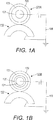
Jede der Aufladungswalzen
Die Aufladungselemente
Die Aufladungswalze
Entsprechend einer Ausführungsform der Erfindung können zusätzliche Schichten, wie zum Beispiel Zwischenschichten und/oder Haft- beziehungsweise Klebstoffschichten, zwischen den in der
Der leitfähige Kern
Die äußere Grundschicht
Das erfindungsgemäße Aufladungselement kann Zwischenschichten und/oder Haft- beziehungsweise Klebstoffschichten umfassen, mit denen die Eigenschaften und die Leistungsfähigkeit des Aufladungselements modifiziert werden können. Beispiele für die Zwischenschichten umfassen Elastomerschichten, wie zum Beispiel eine leitfähige Gummi-Zwischenschicht, die beispielsweise aus Silikon, EPDM, Urethan, Epichlorhydrin oder dergleichen hergestellt wurde. Beispiele für die Haft- beziehungsweise Klebstoffschichten umfassen Schichten, die aus einem Epoxyharz oder aus einem Polysiloxan hergestellt wurden. Die Haft- beziehungsweise Klebstoffe können handelsüblich erhältliche Materialien sein, wie beispielsweise THIXON 403/404, Union Carbide A-1100, Dow H41, Dow TACTIX 740, Dow TACTIX 741 oder Dow TACTIX 742.The charging element according to the invention may comprise intermediate layers and / or adhesive layers with which the properties and the performance of the charging element can be modified. Examples of the intermediate layers include elastomer layers such as a conductive rubber intermediate layer made of, for example, silicone, EPDM, urethane, epichlorohydrin or the like. Examples of the adhesive layers include layers made of an epoxy resin or a polysiloxane. The adhesives may be commercially available materials such as THIXON 403/404, Union Carbide A-1100, Dow H41, Dow TACTIX 740, Dow TACTIX 741 or Dow TACTIX 742.
Das erfindungsgemäße Aufladungselement kann nicht nur eine Walze sein, sondern auch ein Band, ein Blatt oder ein Drelt, das zum Aufladen eines lichtempfindlichen Elements verwendet werden kann und das die Materialien umfasst, die zuvor in Zusammenhang mit den Aufladungswalzen
Das erfindungsgemäße Aufladungselement 120A/B umfasst eine äußere Oberflächenbeschichtung
Die Füllstoffteilchen
Die elektrisch leitfähigen oder halbleitenden Füllstoffteilchen
Die äußeren Oberflächenbeschichtung
Entsprechend einer bevorzugten Ausführungsform der Erfindung ist das Polymer ein thermoplastisches Polycaprolacton mit einem gewichtsgemittelten Molekulargewicht im Bereich von etwa 10000 bis etwa 80000, etwa 20000 bis etwa 50000 oder etwa 25000 bis etwa 45000. Beispiele für handelsüblich erhältliche thermoplastische Polycaprolactone umfassen Capa® 6250 und Capa® 6100 (Perstorp AB, Perstorp, Schweden, und/oder Perstorp USA, Toledo, Ohio).According to a preferred embodiment of the invention the polymer is a thermoplastic polycaprolactone having a weight average molecular weight ranging from about 10,000 to about 80,000, about 20,000 to about 50,000 or about 25,000 to about 45000. Examples of commercially available thermoplastic polycaprolactones include Capa ® 6250 and Capa ® 6100 (Perstorp AB, Perstorp, Sweden, and / or Perstorp USA, Toledo, Ohio).
Entsprechend einer anderen bevorzugten Ausführungsform der Erfindung ist das Polymer ein Copolymer mit Monomereinheiten, abgeleitet von konjugierten Dienmonomeren, aromatischen Vinylmonomeren und/oder ethylenisch ungesättigten Nitrilmonomeren. Beispiele für solche Copolymere umfassen Styrol-Butadien(SB)-Copolymere, Acrylnitril-Butadien(NBR)-Copolymere, Acrylnitril-Butadien-Styrol(ABS)-Terpolymere und dergleichen, sowie Gemische davon. Entsprechend einer besonders bevorzugten Ausführungsform der Erfindung ist das Polymer, das in der äußeren Oberflächenbeschichtung
Das thermoplastische oder thermisch aushärtbare Polymer, das in der äußeren Oberflächenbeschichtung
Das Polymer, das in der äußeren Oberflächenbeschichtung
Beispiele für die Phenolquellen umfassen Phenol; Alkyl-substituierte Phenole, wie beispielsweise Kresole oder Xylenole; Halogen-substituierte Phenole, wie beispielsweise Chlorphenol; Phenole mit mehreren Hydroxygruppen, wie beispielsweise Resorzin oder Brenzcatechin; polycyclische Phenole, wie beispielsweise Naphthol oder Eisphenol A; Aryl-substituierte Phenole; Cycloalkyl-substituierte Phenole; Aryloxy-substituierte Phenole; und dergleichen, sowie Gemische davon. Beispiele für spezifische Phenolquellen umfassen Phenol, 2,6-Xylenol, o-Kresol, p-Kresol, 3,5-Xylenol, 3,4-Xylenol, 2,3,4-Trimethylphenol, 3-Ethylphenol, 3,5-Diethylphenol, p-Butylphenol, 3,5-Dibutylphenol, p-Amylphenol, p-Cyclohexylphenol, p-Octylphenol, 3,5-Dicyclohexylphenol, p-Phenylphenol, p-Crotylphenol, 3,5-Dimethoxyphenol, 3,4,5-Trimethoxyphenol, p-Ethoxyphenol, p-Butoxyphenol, 3-Methyl-4-methoxyphenol, p-Phenoxyphenol, Phenole mit mehreren Ringen wie beispielsweise Bisphenol A, und Gemische davon.Examples of the phenol sources include phenol; Alkyl-substituted phenols, such as cresols or xylenols; Halogen-substituted phenols such as chlorophenol; Multi-hydroxy phenols such as resorcin or catechol; polycyclic phenols, such as naphthol or bisphenol A; Aryl-substituted phenols; Cycloalkyl-substituted phenols; Aryloxy-substituted phenols; and the like, as well as mixtures thereof. Examples of specific sources of phenol include phenol, 2,6-xylenol, o-cresol, p-cresol, 3,5-xylenol, 3,4-xylenol, 2,3,4-trimethylphenol, 3-ethylphenol, 3,5-diethylphenol , p-butylphenol, 3,5-dibutylphenol, p-amylphenol, p-cyclohexylphenol, p-octylphenol, 3,5-dicyclohexylphenol, p-phenylphenol, p-crotylphenol, 3,5-dimethoxyphenol, 3,4,5-trimethoxyphenol , p-ethoxyphenol, p-butoxyphenol, 3-methyl-4-methoxyphenol, p-phenoxyphenol, multi-ring phenols such as bisphenol A, and mixtures thereof.
Beispiele für die Aldehyde, die für die Herstellung der Phenolharze verwendet werden können, umfassen Formaldehyd, Paraformaldehyd, Acetaldehyd, Butyraldehyd, Paraldehyd, Glyoxal, Furfuraldehyd, Propionaldehyd, Benzaldehyd und Gemische davon. Ein bevorzugter Aldehyd ist Formaldehyd. Examples of the aldehydes that can be used for the preparation of the phenolic resins include formaldehyde, paraformaldehyde, acetaldehyde, butyraldehyde, paraldehyde, glyoxal, furfuraldehyde, propionaldehyde, benzaldehyde, and mixtures thereof. A preferred aldehyde is formaldehyde.
Beispiele für die Phenolharze umfassen Phenolharze vom Dicyclopentadien-Typ, Phenol-Novolak-Harze, Kresol-Novolak-Harze, Phenol-Aralkyl-Harze und Gemische davon. Beispiele für andere Phenolharze umfassen alkohollösliche Phenolharze vom Resol-Typ, wie zum Beispiel PHENOLOTE® J-325 (DIC Corp., Tokyo, Japan); Formaldehydpolymere mit Phenol, p-tert-Butylphenol und Kresol, wie zum Beispiel VARCUMTM 29159 und 29101 (OxyChem Co.) und DURITE® 97 (Borden Chemical); oder Formaldehydpolymere mit Ammoniak, Kresol und Phenol, wie zum Beispiel VARCUM® 29112 (OxyChem Co.); oder Formaldehydpolymere mit 4,4'-(1-Methylethyliden)bisphenol, wie zum Beispiel VARCUM® 29108 und 29116 (OxyChem Co.); oder Formaldehydpolymere mit Kresol und Phenol, wie zum Beispiel VARCUMTM 29457 (OxyChem Co.), DURITE® SD-423A, SD-422A (Borden Chemical); oder Formaldehydpolymere mit Phenol und p-tert-Butylphenol, wie zum Beispiel DURITE® ESD 556C (Border Chemical).Examples of the phenol resins include dicyclopentadiene type phenol resins, phenol novolac resins, cresol novolak resins, phenol aralkyl resins, and mixtures thereof. Examples of other phenolic resins include alcohol-soluble phenolic resins, resol-type, such as ® PHENOLOTE J-325 (DIC Corp., Tokyo, Japan); Formaldehyde polymers with phenol, p-tert-butylphenol and cresol, such as VARCUM 29159 and 29101 TM (OxyChem Co.), and DURITE 97 ® (Borden Chemical); or formaldehyde polymers with ammonia, cresol and phenol, such as VARCUM ® 29112 (OxyChem Co.); or formaldehyde polymers with 4,4 '- (1-methylethylidene) bisphenol, such as VARCUM ® 29108 and 29116 (OxyChem Co.); or formaldehyde polymers with cresol and phenol, such as VARCUM TM 29457 (OxyChem Co.), DURITE SD-423A ®, SD-422A (Borden Chemical); or formaldehyde polymers with phenol and p-tert-butylphenol, such as DURITE ESD ® 556C (Border Chemical).
Die Phenolharze können als solche oder in modifizierter Form verwendet werden. Die Phenolharze können beispielsweise mit geeigneten Weichmachern modifiziert werden, und Beispiele dafür umfassen Polyvinylbutyral, Nylonharze, thermische aushärtbare Acrylharze, Polyvinylformal, Alkydverbindungen, Epoxyharze, Phenoxyharze (Bisphenol A, Epichlorhydrinpolymere oder dergleichen), Polyamide, Polyacrylate, Öle und dergleichen, sowie Gemische davon. Verschiedenste bekannte Modifizierungsmittel sind unter den Handelsnamen DESMOPHEN®, DESMODUR®, BUTVAR®, ELVAMIDE®, DORESCO®, SILCLEAN® oder PARALOID® erhältlich.The phenolic resins can be used as such or in modified form. For example, the phenolic resins may be modified with suitable plasticizers, and examples thereof include polyvinyl butyral, nylon resins, thermosetting acrylic resins, polyvinyl formal, alkyd compounds, epoxy resins, phenoxy resins (bisphenol A, epichlorohydrin polymers or the like), polyamides, polyacrylates, oils and the like, as well as mixtures thereof. Various known modifiers are available under the trade name DESMOPHEN ®, DESMODUR ®, BUTVAR ®, ELVAMIDE ®, DORESCO ®, SILCLEAN ® or Paraloid ®.
Das Polymer, das in der äußeren Oberflächenbeschichtung
Wenn Melamin verwendet wird, dann wird das erhaltene Aminoplastharz als ”'Melaminharz” bezeichnet. Verschiedenste Melaminharze sind unter den Handelsnamen CYMEL®, BEETLE®, DYNOMIN®, BECKAMINE®, UFR®, BAKELITE®, ISOMIN®, MELAICAR®, MELBRITE®, MELMEX®, MELOPAS®, RESART® oder ULTRAPAS® erhältlich.When melamine is used, the resulting aminoplast resin is referred to as "melamine resin". Various melamine resins are commercially available under the trade names of CYMEL ®, BEETLE ®, Dynomin ®, BECKAMINE ®, UFR ®, BAKELITE ®, IsoMin ®, MELAICAR ®, MELBRITE ®, MELMEX ®, MELOPAS ®, Resart ® or Ultrapas ®.
Das Melaminharz kann eine Verbindung sein, die durch die folgende Formel dargestellt wird: 
Das Melaminharz kann eine Verbindung sein, die wasserlöslich, dispergierbar oder nicht dispergierbar ist. Das Melaminharz kann hochgradig alkyliert/alkoxyliert, partiell alkyliert/alkoxyliert oder sowohl alkyliert als auch alkoxyliert sein. Das Melaminharz kann beispielsweise methyliert, n-butyliert oder isobutyliert sein. Das Melaminharz kann wenig Methylolgruppen und viele Iminogruppen enthalten. Das Melaminharz kann eine oligomere Verbindung sein, die als wesentliche funktionelle Gruppen Methoxymethyl- und Iminogruppen enthält. Beispiele für die Melaminharze umfassen methylierte Melaminharze mit einem hohen Gehalt an Iminogruppen (partiell methylolierte und hochgradig alkylierte Verbindungen), wie beispielsweise CYMEL® 323, 325, 327, 328, 385; hochgradig methylierte Melaminharze, wie beispielsweise CYMEL® 350, 9370; partiell methylierte Melaminharze (hochgradig methylolierte und partiell methylierte Verbindungen), wie beispielsweise CYMEL® 373, 370; gemischte Ether-Melaminharze mit einem hohen Feststoffanteil, wie beispielsweise CYMEL® 1130, 324; n-butylierte Melaminharze, wie beispielsweise CYMELTM 1151, 615; n-butylierte Melaminharze mit einem hohen Gehalt an Iminogruppen, wie beispielsweise CYMEL® 1158; und isobutylierte Melaminharze, wie beispielsweise CYMEL® 255-10. Melaminharze mit dem Handelsnamen CYMEL® sind handelsüblich erhältlich von Cytec Industries Inc., Woodland Park, NJ.The melamine resin may be a compound that is water-soluble, dispersible or non-dispersible. The melamine resin can be highly alkylated / alkoxylated, partially alkylated / alkoxylated or both alkylated as also be alkoxylated. The melamine resin may be, for example, methylated, n-butylated or isobutylated. The melamine resin may contain few methylol groups and many imino groups. The melamine resin may be an oligomeric compound containing methoxymethyl and imino groups as essential functional groups. Examples of the melamine resins include methylated melamine resins having a high content of imino groups (partially methylolated and highly alkylated compounds) such as CYMEL ® 323, 325, 327, 328, 385; highly methylated melamine resins such as CYMEL ® 350, 9370; partially methylated melamine resins (highly methylolated and partially methylated compounds), such as CYMEL ® 373, 370; mixed ether melamine resins with a high solids content, such as CYMEL ® 1130, 324; n-butylated melamine resins such as CYMEL ™ 1151, 615; n-butylated melamine resins with a high content of imino groups, such as CYMEL ® 1158; and isobutylated melamine resins such as CYMEL ® 255-10. Melamine resins with the trademark CYMEL ® are commercially available from Cytec Industries Inc., Woodland Park, NJ.
Entsprechend einer Ausführungsform der Erfindung sind die Melaminharze ausgewählt aus methylierten Formaldehyd-Melamin-Harzen, methoxymethylierten Melaminharzen, ethoxymethylierten Melaminharzen, propoxymethylierten Melaminharzen, butoxymethylierten Melaminharzen, Hexamethylolmelaminharzen, alkoxyalkylierten Melaminharzen wie beispielsweise methoxymethylierten Melaminharzen, ethoxymethylierten Melaminharzen, propoxymethylierten Melaminharzen, butoxymethylierten Melaminharzen, und Gemischen davon.According to one embodiment of the invention, the melamine resins are selected from methylated formaldehyde-melamine resins, methoxymethylated melamine resins, ethoxymethylated melamine resins, propoxymethylated melamine resins, butoxymethylated melamine resins, hexamethylolmelamine resins, alkoxyalkylated melamine resins such as methoxymethylated melamine resins, ethoxymethylated melamine resins, propoxymethylated melamine resins, butoxymethylated melamine resins, and mixtures thereof ,
Wenn Harnstoff verwendet wird, dann wird das erhaltene Aminoplastharz als ”Harnstoffharz” bezeichnet. Verschiedenste Harnstoffharze sind unter den Handelsnamen CYMEL®, BEETLE®, DYNOMIN®, BECKAMINE® oder AMIREME® erhältlich.When urea is used, the resulting aminoplast resin is called a "urea resin". Various urea resins are commercially available under the tradenames CYMEL ®, BEETLE ®, Dynomin ®, BECKAMINE ® or AMIREME ®.
Das Harnstoffharz kann eine Verbindung sein, die durch die folgende Formel dargestellt wird: 
Das Harnstoffharz kann eine Verbindung sein, die wasserlöslich, dispergierbar oder nicht dispergierbar ist. Das Harnstoffharz kann hochgradig alkyliert/alkoxyliert, partiell alkyliert/alkoxyliert oder sowohl alkyliert als auch alkoxyliert sein. Das Harnstoffharz kann beispielsweise methyliert, n-butyliert oder isobutyliert sein. Beispiele für die Harnstoffharze umfassen methylierte Harnstoffharze, wie beispielsweise CYMEL® U-65, U-382; n-butylierte Harnstoffharze, wie beispielsweise CYMEL® U-1054, UB-30-B; und isobutylierte Harnstoffharze, wie beispielsweise CYMEL® U-662, UI-19-I. Harnstoffharze mit dem Handelsnamen CYMEL® sind handelsüblich erhältlich von Cytec industries Inc., Woodland Park, NJ.The urea resin may be a compound that is water-soluble, dispersible or non-dispersible. The urea resin can be highly alkylated / alkoxylated, partially alkylated / alkoxylated, or both alkylated and alkoxylated. The urea resin may be, for example, methylated, n-butylated or isobutylated. Examples of the urea resin include methylated urea resins such as CYMEL ® U-65, U-382; n-butylated urea resins such as CYMEL ® U-1054, UB-30-B; and isobutylated urea resins such as CYMEL ® U-662, UI-19-I. Urea resins having the trade name CYMEL ® are commercially available from Cytec Industries Inc., Woodland Park, NJ.
Wenn Benzoguanamin verwendet wird, dann wird das erhaltene Aminoplastharz als ”Benzoguanaminharz” bezeichnet. Verschiedenste Benzoguanaminharze sind unter den Handelsnamen CYMEL®, BEETLE® oder UFORMITE® erhältlich.When benzoguanamine is used, the obtained aminoplast resin is called "benzoguanamine resin". Various benzoguanamine are available under the tradenames CYMEL ®, BEETLE ® or UFORMITE ®.
Das Benzoguanaminharz kann eine Verbindung sein, die durch die folgende Formel dargestellt wird: 
Das Benzoguanaminharz kann eine Verbindung sein, die wasserlöslich, dispergierbar oder nicht dispergierbar ist. Das Benzoguanaminharz kann hochgradig alkyliert/alkoxyliert, partiell alkyliert/alkoxyliert oder sowohl alkyliert als auch alkoxyliert sein. Das Benzoguanaminharz kann beispielsweise methyliert, n-butyliert oder isobutyliert sein, Beispiele für die Benzoguanaminharze umfassen CYMEL® 659, 5010, 5011. Benzoguanaminharze mit dem Handelsnamen CYMEL® sind handelsüblich erhältlich von
Wenn Glycouracil verwendet wird, dann wird das erhaltene Aminoplastharz als ”Glycolurilharz” bezeichnet. Verschiedenste Glycolurilharze sind unter den Handelsnamen CYMEL® oder POWDERLINK® erhältlich.When glycouracil is used, the resulting aminoplast resin is referred to as "glycoluril resin". Various glycoluril is available under the tradenames CYMEL ® or POWDER LINK ®.
Das Glycolurilharz kann eine Verbindung sein, die durch die folgende Formel dargestellt wird: 
Das Glycolurilharz kann eine Verbindung sein, die wasserlöslich, dispergierbar oder nicht dispergierbar ist. Das Glycolurilharz kann hochgradig alkyliert/alkoxyliert, partiell alkyliert/alkoxyliert oder sowohl alkyliert als auch alkoxyliert sein. Das Glycolurilharz kann beispielsweise methyliert, n-butyliert oder isobutyliert sein. Beispiele für die Glycolurilharze umfassen CYMEL® 1170, 1171. Glycolurilharze mit dem Handelsnamen CYMEL® sind handelsüblich erhältlich von
Die Fluor-enthaltenden Polymere oder Fluorpolymere, die in der äußeren Oberflächenbeschichtung 129, 129A/B verwendet werden können, können zum Beispiel in Form von Fluorpolymerteilchen vorliegen. Diese Fluorpolymere können beispielsweise sich wiederholende Monomereinheiten enthalten, die von Vinylidenfluorid, Hexafluorpropylen, Tetrafluorethylen, Perfluoralkylvinylethern und Gemischen davon abgeleitet sind. Die Fluorpolymere können geradkettige oder verzweigte Polymere oder vernetzte Fluorelastomere sein. Beispiele für die Fluorpolymere umfassen Polytetrafluorethylen (PTFE); Perfluoralkoxypolymerharze (PFA); Copolymere aus Tetrafluorethylen (TFE) und Hexafluorpropylen (HFP); Copolymere aus Hexafluorpropylen (HFP) und Vinylidenfluorid (VDF oder VF2); Terpolymere aus Tetrafluorethylen (TFE), Vinylidenfluorid (VDF) und Hexafluorpropylen (HFP); Tetrapolymere aus Tetrafluorethylen (TFE), Vinylidenfluorid (VF2), Hexafluorpropylen (HFP) und einem weiteren Monomer; und Gemische davon. Die Fluorpolymere und/oder die Fluorpolymerteilchen haben eine niedrige Oberflächenenergie und verleihen der äußeren Oberflächenbeschichtung chemische und thermische Beständigkeit. Die Fluorpolymere und/oder die Fluorpolymerteilchen können eine Schmelztemperatur im Bereich von etwa 255°C bis etwa 360°C oder im Bereich von etwa 280°C bis etwa 330°C haben. Entsprechend einer Ausführungsform der Erfindung können die Fluorpolymere und/oder die Fluorpolymerteilchen geschmolzen werden, um die äußere Oberflächenbeschichtung herzustellen.The fluorine-containing polymers or fluoropolymers that may be used in
Die äußere Oberflächenbeschichtung
Eine Dispersion, umfassend den leitfähigen Füllstoff und ein Polymer oder mehrere Polymere (beispielsweise PCL), kann zum Beispiel hergestellt werden, indem die Bestandteile in einem Lösungsmittel (beispielsweise Toluol) in einer Kugelmühle miteinander vermischt werden. Dieser Prozess kann mehrere Tage lang dauern. Die Dispersion kann einen Feststoffgehalt von etwa 5 Gewichtsprozent bis etwa 60 Gewichtsprozent, etwa 10 Gewichtsprozent bis etwa 50 Gewichtsprozent oder etwa 20 Gewichtsprozent bis etwa 40 Gewichtsprozent haben. Die Dispersion kann dann auf dem leitfähigen Substrat einer Aufladungswalze zum Übertragen einer Vorspannung, auf einer Zwischenschicht einer Aufladungswalze, auf einer Haft- beziehungsweise Klebstoffschicht einer Aufladungswalze oder auf einer herkömmlichen äußeren Grundschicht einer herkömmlichen Aufladungswalze zum Übertragen einer Vorspannung aufgebracht werden. Beispiele für geeignete Beschichtungsverfahren umfassen das Eintauchbeschichten, das Beschichten mit einer Walze, das Sprühbeschichten, das Beschichten mit einem Rotationszerstäuber, das Beschichten mit einem Ring, das Schmelzbeschichten, das Fließbeschichten und dergleichen. Die aufgebrachte Dispersion kann dann verfestigt werden (beispielsweise durch Aushärten oder Trocknen); die Bedingungen beim Verfestigen hängen von der Art der verwendeten Polymere ab.For example, a dispersion comprising the conductive filler and one or more polymers (for example, PCL) can be prepared by mixing the ingredients together in a solvent (for example, toluene) in a ball mill. This process can take several days. The dispersion may have a solids content of from about 5 weight percent to about 60 weight percent, from about 10 weight percent to about 50 weight percent, or from about 20 weight percent to about 40 weight percent. The dispersion may then be applied to the conductive substrate of a charge roller for transferring a bias, to an intermediate layer of a charge roller, to an adhesive layer of a charge roller or to a conventional outer base layer of a conventional charge roller for transferring a bias voltage. Examples of suitable coating methods include dip coating, roller coating, spray coating, rotary atomizer coating, ring coating, melt coating, flow coating, and the like. The applied dispersion can then be solidified (for example, by curing or drying); the conditions of solidification depend on the type of polymers used.
Es kann auch eine Dispersion hergestellt werden, welche den leitfähigen Füllstoff und eine Vielzahl von Polymerteilchen enthält. Die Dispersion mit den Polymerteilchen kann mit dem leitfähigen Füllstoff vermischt werden. Das Gemisch mit dem leitfähigen Füllstoff und den Polymerteilchen kann so hergestellt werden, dass der Feststoffgehalt innerhalb der zuvor angegebenen Bereiche liegt.A dispersion containing the conductive filler and a plurality of polymer particles may also be prepared. The dispersion with the polymer particles may be mixed with the conductive filler. The mixture with the conductive filler and the polymer particles may be prepared so that the solids content is within the ranges given above.
Entsprechend einer Ausführungsform der Erfindung kann die Dispersion mit den leitfähigen Füllstoffteilchen und den Polymerteilchen auf einem leitfähigen Substrat, auf einer Zwischenschicht, auf einer Haft- beziehungsweise Klebstoffschicht oder auf einer äußeren Grundschicht einer Aufladungswalze zum Übertragen einer Vorspannung aufgebracht werden. Die Polymerteilchen in der aufgebrachten Dispersion können dann zumindest teilweise geschmolzen werden, und danach kann der Überzug abgekühlt werden. Dieses teilweise Schmelzen der Polymerteilchen führt zur Bildung einer Polymermatrix
Entsprechend einer anderen Ausführungsform der Erfindung kann die Dispersion mit dem leitfähigen Füllstoff und den Polymerteilchen mit einem zweiten Polymer vermischt werden. Dieses Vermischen kann in einer Kugelmühle in einem geeigneten Lösungsmittel, das in Abhängigkeit von der Art der verwendeten Polymere ausgewählt wird, durchgeführt werden. Das zweite Polymer und die Polymerteilchen können aus den gleichen oder aus unterschiedlichen Polymeren bestehen. Die Dispersion mit den leitfähigen Füllstoffteilchen, den Polymerteilchen und dem zweiten Polymer kann einen Feststoffgehalt von etwa 5 Gewichtsprozent bis etwa 60 Gewichtsprozent, etwa 10 Gewichtsprozent bis etwa 50 Gewichtsprozent oder etwa 20 Gewichtsprozent bis etwa 40 Gewichtsprozent haben. Die Dispersion kann dann auf einem leitfähigen Substrat, auf einer Zwischenschicht, auf einer Haft- beziehungsweise Klebstoffschicht oder auf einer äußeren Grundschicht einer Aufladungswalze zum Übertragen einer Vorspannung aufgebracht werden, wobei verschiedenste Beschichtungsverfahren angewandt werden können. Die aufgebrachte Dispersion kann dann verfestigt werden (beispielsweise durch Aushärten oder Trocknen); die Bedingungen beim Verfestigen hängen von der Art der verwendeten Polymere ab. Auf diese Weise wird eine äußere Oberflächenbeschichtung
Entsprechend einer weiteren Ausführungsform der Erfindung kann eine Dispersion mit dem leitfähigen Füllstoff und den Polymeren mit einem bestimmten Feststoffgehalt auf der Oberfläche eines separaten Substrats aufgebracht werden. Die aufgebrachte Dispersion wird dann verfestigt, und die erhaltene Schicht wird danach vom Substrat entfernt und dann als äußere Oberflächenbeschichtung
Die Oberflächeneigenschaften sowie die elektrischen, mechanischen und/oder strukturellen Eigenschaften der erhaltenen Aufladungselemente zum Übertragen einer Vorspannung hängen von der Art und von der Menge der Füllstoffe und Polymere, die in der äußeren Grundschicht
Die Oberflächenrauhigkeit (Rz) der äußeren Oberflächenbeschichtung, die auf der äußeren Grundschicht aufgebracht ist, kann erfindungsgemäß so eingestellt werden, dass eine gleichförmige Aufladung über mehrere tausend Zyklen möglich ist und eine Ansammlung von Abriebteilchen oder Fremdstoffen an der Oberfläche des Aufladungselements verhindert wird. Die erfindungsgemäße Oberflächenbeschichtung hat eine verbesserte Abriebbeständigkeit, wird nicht so leicht beschädigt und verhindert eine Ansammlung von teilchenförmigen Materialien an der Oberfläche des Aufladungselements, so dass einwandfreie beziehungsweise fehlerfreie Ausdrucke erhalten werden.The surface roughness (R z ) of the outer surface coating applied on the outer base layer can be adjusted according to the invention so as to allow uniform charging for several thousand cycles and prevent accumulation of debris or foreign matter on the surface of the charging member. The surface coating of the present invention has improved abrasion resistance, is not easily damaged, and prevents accumulation of particulate materials on the surface of the charging member, so that flawless prints are obtained.
Die äußere Grundschicht
Die äußere Oberflächenbeschichtung
Die Dimensionen und/oder die elektrischen, mechanischen und/oder sonstigen Eigenschaften der äußeren Grundschicht und/oder der äußeren Oberflächenbeschichtung sind jedoch nicht auf bestimmte Werte beschränkt.However, the dimensions and / or the electrical, mechanical and / or other properties of the outer base layer and / or the outer surface coating are not limited to specific values.
Die Oberflächenrauhigkeit Rz ist ein Wert, der mit einer 10-Punkte-Messung entsprechend dem
Die erfindungsgemäße äußere Oberflächenbeschichtung und/oder Schichtanordnung dient ebenfalls als Schutzschicht für das Aufladungselement, wodurch die Probleme gelöst werden, die sich aus dem direkten Kontakt des Aufladungselements mit anderen Elementen des Druckers ergeben. Durch die Verwendung der erfindungsgemäßen äußeren Oberflächenbeschichtung/Schichtanordnung kann das lichtempfindliche Element gleichmäßig aufgeladen werden, was mit einem herkömmlichen Aufladungselement zum Übertragen einer Vorspannung ohne die erfindungsgemäße äußere Oberflächenbeschichtung/Schichtanordnung nicht möglich ist. Die Druckqualität kann folglich verbessert werden, wenn die erfindungsgemäße äußere Oberflächenbeschichtung/Schichtanordnung verwendet wird. The outer surface coating and / or layer arrangement according to the invention also serves as a protective layer for the charging element, which solves the problems resulting from the direct contact of the charging element with other elements of the printer. By using the outer surface coating / layer arrangement according to the invention, the photosensitive element can be uniformly charged, which is not possible with a conventional charging element for transmitting a bias without the outer surface coating / layer arrangement according to the invention. The print quality can thus be improved if the outer surface coating / layer arrangement according to the invention is used.
Die äußere Oberflächenbeschichtung/Schichtanordnung kann auch zum Erneuern einer herkömmlichen Aufladungswalze zum Übertragen einer Vorspannung oder zum Erneuern der erfindungsgemäßen Aufladungswalze selbst verwendet werden. Wenn die äußere Oberfläche einer Aufladungswalze so beschädigt ist, dass keine akzeptablen Ausdrucke mehr erhalten werden, kann die Aufladungswalze erneuert werden. Das Erneuern kann das Aufbringen der erfindungsgemäßen äußeren Oberflächenbeschichtung/Schichtanordnung umfassen. Wenn die schützende äußere Oberflächenbeschichtung/Schichtanordnung auf eine Aufladungswalze mit einer beschädigten Oberfläche, die bereits eine Schutzschicht umfassen kann, aufgebracht wird, kann die Aufladungswalze über einen längeren Zeitraum hinweg verwendet werden.The outer surface coating / layer assembly may also be used to renew a conventional charging roll for transferring a bias or renewing the charging roll itself. If the outer surface of a charge roller is so damaged that acceptable printouts are no longer obtained, the charge roller can be renewed. Refurbishing may include applying the outer surface coating / layer assembly of the present invention. When the protective outer surface coating / layer assembly is applied to a charging roller having a damaged surface which may already comprise a protective layer, the charging roller may be used for an extended period of time.
BeispieleExamples
Es wurden Dispersionen hergestellt, indem ein Polymer oder mehrere Polymere mit Ruß in einer Kugelmühle miteinander vermischt wurden. In der folgenden Tabelle 1 sind unterschiedliche Zusammensetzungen angegeben, die unter Verwendung des Rußes Vulcan XC72 (Cabot Corp., Boston, MA) hergestellt wurden. Für die Herstellung jeder Dispersion wurden 1/8'' Edelstahlkügelchen als Mahlmedium zu dem Gemisch gegeben und das Gemisch wurde dann etwa 3 Tage lang gemahlen. Danach wurden die Edelstahlkügelchen durch Abfiltrieren entfernt, und die Dispersion wurde dann unter Verwendung eines Tsukiage-Beschichters in einer Dicke von etwa 6 μm auf einer Imari-Aufladungswalze aufgebracht. Die beschichtete Walze wurde dann etwa 15 Minuten lang bei etwa 140°C in einem Heißluftstromofen getrocknet, wobei eine erfindungsgemäße Aufladungswalze zum Übertragen einer Vorspannung erhalten wurde. Der spezifische elektrische Oberflächenwiderstand (beispielsweise gemessen mit der Prüfvorrichtung Hiresta UP Resistivity Meter) und die Oberflächenrauhigkeit (beispielsweise gemessen mit der Prüfvorrichtung Perthometer) jeder der erhaltenen Beschichtungen sind in der Tabelle 1 angegeben. Tabelle 1
Die in der Tabelle 1 angegebenen äußeren Oberflächenbeschichtungen enthielten:
- (A): B98 (Härtungsmittel)/CYMEL® 325 (Melaminharz)
- (B): DORESCO® TA-228/CYMEL® 1170
- (C): Blendex 200 (ABS-Copolymer)
- (A): B98 (curing agent) / CYMEL ® 325 (melamine resin)
- (B): DORESCO ® TA-228 / CYMEL ® 1170
- (C): Blendex 200 (ABS copolymer)
Die Gleichmäßigkeit der elektrischen Ladung der hergestellten Aufladungswalzen mit den Oberflächenbeschichtungen (A) bis (C) wurde sowohl vor als auch nach einem 50000 Zyklen-Verschleißtest in einer Hodaka-Prüfvorrichtung ermittelt. Die Gleichmäßigkeit der elektrischen Ladung jeder der hergestellten erfindungsgemäßen Aufladungswalzen war besser als die einer Vergleichsaufladungswalze, die keine erfindungsgemäße Beschichtung umfasste. Eine Ansammlung von elektrischer Ladung oder eine Verschlechterung der Ladungskapazität wurde bei den hergestellten erfindungsgemäßen Aufladungswalzen nicht beobachtet.The uniformity of the electric charge of the manufactured supercharger rolls having the surface coatings (A) to (C) was determined both before and after a 50,000 cycle wear test in a hodaka tester. The uniformity of the electric charge of each of the charging rollers of the invention prepared was better than that of a comparative charging roller which did not include a coating of the present invention. Accumulation of electric charge or deterioration of the charged capacity was not observed in the produced charging rolls of the invention.
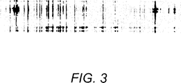
Nachdem die hergestellten erfindungsgemäßen Aufladungswalzen einem 50000 Zyklen-Verschleißtest in einer Hodaka-Prüfvorrichtung unterworfen worden waren, wurden sie verwendet, um Ausdrucke eines eingescannten Bildes herzustellen. Dabei wurden nur fehlerfreie Ausdrucke erhalten, was darauf hindeutet, dass die Aufladungswalzen beim Verschleißtest nicht abgerieben oder verkratzt oder auf andere Art und Weise oberflächlich beschädigt worden waren und dass sich keine Tonerrückstände an der Oberfläche der Aufladungswalzen angesammelt hatten. Wenn jedoch eine Vergleichsaufladungswalze, die keine erfindungsgemäße äußere Oberflächenbeschichtung/Schichtanordnung umfasste, für die Herstellung von Ausdrucken eines eingescannten Bildes verwendet wurde, hatten die Ausdrucke deutliche Streifen, wie in der
ZITATE ENTHALTEN IN DER BESCHREIBUNG QUOTES INCLUDE IN THE DESCRIPTION
Diese Liste der vom Anmelder aufgeführten Dokumente wurde automatisiert erzeugt und ist ausschließlich zur besseren Information des Lesers aufgenommen. Die Liste ist nicht Bestandteil der deutschen Patent- bzw. Gebrauchsmusteranmeldung. Das DPMA übernimmt keinerlei Haftung für etwaige Fehler oder Auslassungen.This list of the documents listed by the applicant has been generated automatically and is included solely for the better information of the reader. The list is not part of the German patent or utility model application. The DPMA assumes no liability for any errors or omissions.
Zitierte Nicht-PatentliteraturCited non-patent literature
- Cytec Industries Inc., Woodland Park, NJ [0040] Cytec Industries Inc., Woodland Park, NJ [0040]
- Cytec Industries Inc., Woodland Park, NJ [0043] Cytec Industries Inc., Woodland Park, NJ [0043]
- Standard JIS B 0601-1982 [0056] Standard JIS B 0601-1982 [0056]
Claims (10)
Applications Claiming Priority (2)
| Application Number | Priority Date | Filing Date | Title |
|---|---|---|---|
| US13/171,361 US8620187B2 (en) | 2011-06-28 | 2011-06-28 | Surface coatings for the bias charging roller |
| US13/171,361 | 2011-06-28 |
Publications (1)
| Publication Number | Publication Date |
|---|---|
| DE102012210186A1 true DE102012210186A1 (en) | 2013-01-03 |
Family
ID=47355334
Family Applications (1)
| Application Number | Title | Priority Date | Filing Date |
|---|---|---|---|
| DE102012210186A Withdrawn DE102012210186A1 (en) | 2011-06-28 | 2012-06-18 | Charging element for transmitting a bias voltage |
Country Status (3)
| Country | Link |
|---|---|
| US (1) | US8620187B2 (en) |
| JP (1) | JP5909408B2 (en) |
| DE (1) | DE102012210186A1 (en) |
Families Citing this family (10)
| Publication number | Priority date | Publication date | Assignee | Title |
|---|---|---|---|---|
| US8768219B2 (en) * | 2009-11-20 | 2014-07-01 | Xerox Corporation | Bias charging overcoat |
| US8649704B2 (en) * | 2009-11-20 | 2014-02-11 | Xerox Corporation | Bias charging overcoat |
| US8609233B2 (en) * | 2010-07-09 | 2013-12-17 | Xerox Corporation | Intermediate transfer member |
| JP6056705B2 (en) * | 2013-08-14 | 2017-01-11 | 富士ゼロックス株式会社 | Charging roll, charging device, process cartridge, image forming apparatus, and manufacturing method of charging roll |
| US9244410B1 (en) * | 2015-02-17 | 2016-01-26 | Xerox Corporation | Fuser member |
| US9869945B2 (en) * | 2015-04-14 | 2018-01-16 | Xerox Corporation | Electrostatic charging member |
| CN105085532B (en) * | 2015-09-07 | 2017-07-04 | 山西医科大学 | A kind of Trimethylmethanaminium chloride Tetramine chloride derivative and preparation method thereof |
| JP7067172B2 (en) * | 2018-03-22 | 2022-05-16 | 富士フイルムビジネスイノベーション株式会社 | Charging member, charging device, process cartridge and image forming device |
| EP3848758A4 (en) * | 2018-09-05 | 2021-10-13 | NOK Corporation | Conductive roll |
| JP7363160B2 (en) * | 2019-07-25 | 2023-10-18 | 京セラドキュメントソリューションズ株式会社 | Image forming device and image forming method |
Family Cites Families (14)
| Publication number | Priority date | Publication date | Assignee | Title |
|---|---|---|---|---|
| US4967231A (en) * | 1987-12-29 | 1990-10-30 | Kabushiki Kaisha Toshiba | Apparatus for forming an electrophotographic latent image |
| US6096395A (en) * | 1992-12-16 | 2000-08-01 | Tokai Rubber Industries, Ltd. | Roll including foam body and method of producing the roll |
| JP3400054B2 (en) * | 1993-05-31 | 2003-04-28 | 株式会社リコー | Image forming device |
| CN1081346C (en) * | 1994-10-03 | 2002-03-20 | 佳能株式会社 | Image forming method |
| US6052549A (en) * | 1994-11-25 | 2000-04-18 | Canon Kabushiki Kaisha | Charging roller, and process cartridge and image-forming apparatus employing the roller |
| US6020054A (en) * | 1995-09-19 | 2000-02-01 | Bridgestone Corporation | Charging member and device |
| US5860046A (en) * | 1996-07-09 | 1999-01-12 | Minolta Co., Ltd. | Charging method and charging device |
| JP3527910B2 (en) * | 1998-08-31 | 2004-05-17 | グンゼ株式会社 | Charging roller type electrophotographic copying machine |
| US6317574B1 (en) * | 1999-02-25 | 2001-11-13 | Canon Kabushiki Kaisha | Charging member, process cartridge, and image forming apparatus |
| JP4424839B2 (en) * | 2000-08-31 | 2010-03-03 | 株式会社ブリヂストン | Charging roller |
| JP2002214876A (en) * | 2001-01-12 | 2002-07-31 | Bridgestone Corp | Electrifying member and electrifying device |
| JP5083940B2 (en) * | 2007-02-20 | 2012-11-28 | 株式会社ブリヂストン | Charging roller and manufacturing method thereof |
| JP2008233442A (en) * | 2007-03-20 | 2008-10-02 | Tokai Rubber Ind Ltd | Charging roll |
| JP5178073B2 (en) * | 2007-07-12 | 2013-04-10 | キヤノン株式会社 | Charging member and charging device |
-
2011
- 2011-06-28 US US13/171,361 patent/US8620187B2/en not_active Expired - Fee Related
-
2012
- 2012-05-30 JP JP2012123656A patent/JP5909408B2/en active Active
- 2012-06-18 DE DE102012210186A patent/DE102012210186A1/en not_active Withdrawn
Non-Patent Citations (2)
| Title |
|---|
| Cytec Industries Inc., Woodland Park, NJ |
| Standard JIS B 0601-1982 |
Also Published As
| Publication number | Publication date |
|---|---|
| JP2013011880A (en) | 2013-01-17 |
| JP5909408B2 (en) | 2016-04-26 |
| US8620187B2 (en) | 2013-12-31 |
| US20130004205A1 (en) | 2013-01-03 |
Similar Documents
| Publication | Publication Date | Title |
|---|---|---|
| DE102012210186A1 (en) | Charging element for transmitting a bias voltage | |
| DE102012208453B4 (en) | Charging element for electrostatic charging and method for its preparation | |
| DE112015001173B4 (en) | Charge component, manufacturing method for charge component, electrophotographic device and process cartridge | |
| DE102012209790A1 (en) | Charging element for transmitting a bias voltage and method for its production | |
| US8483591B2 (en) | Bias charging overcoat | |
| DE102004004575A1 (en) | Semiconducting roller | |
| KR100494991B1 (en) | A method for recycling a charging member, the charging member, and an apparatus for recycling the charging member | |
| JP2009031758A (en) | Charging roll | |
| JP6576709B2 (en) | Conductive member for electrophotographic equipment | |
| DE69932367T2 (en) | Transfer element coatings containing soot mixtures | |
| DE102016205258A1 (en) | ELECTROSTATIC LOADING ELEMENT | |
| WO2009087208A1 (en) | Toner roller with an insulation layer which comprises polymer | |
| JP5166810B2 (en) | Developing roll for electrophotographic equipment | |
| DE102016002024A1 (en) | Conductive roller and method of making the roller | |
| JP5176264B2 (en) | Electrophotographic charging member and electrophotographic image forming apparatus using the same | |
| US10025233B2 (en) | Electroconductive member and electrophotographic apparatus | |
| JP3661197B2 (en) | Semi-conductive roll | |
| DE1797368A1 (en) | Electrophotographic imaging plate | |
| CN106019887A (en) | Charging member, process cartridge, and image forming apparatus | |
| JP2007025647A (en) | Electrophotographic charging member and electrophotographic image forming apparatus | |
| JPH04284476A (en) | Electrical conductive coating material | |
| JPH04103672A (en) | Electroconductive paint | |
| JPH06161229A (en) | Conductive roll | |
| JP2006350074A (en) | Electrifying member for electrophotography and electrophotographic image forming apparatus using the same | |
| JPH06208288A (en) | Electric conductive roller |
Legal Events
| Date | Code | Title | Description |
|---|---|---|---|
| R012 | Request for examination validly filed | ||
| R079 | Amendment of ipc main class |
Free format text: PREVIOUS MAIN CLASS: G03G0005000000 Ipc: G03G0015020000 |
|
| R016 | Response to examination communication | ||
| R119 | Application deemed withdrawn, or ip right lapsed, due to non-payment of renewal fee |