Hintergrund der ErfindungBackground of the invention
Gebiet der ErfindungField of the invention
Die vorliegende Erfindung betrifft eine Stromversorgungsvorrichtung und eine Druckvorrichtung. Insbesondere betrifft die vorliegende Erfindung eine Stromversorgungsvorrichtung und eine Druckvorrichtung, die ein Bild auf einem Druckmedium mit Hilfe eines Tintenstrahl-Druckkopfs druckt und die Stromversorgungsvorrichtung verwendet.The present invention relates to a power supply device and a printing device. More particularly, the present invention relates to a power supply device and a printing device that prints an image on a print medium by means of an ink jet print head and uses the power supply device.
Beschreibung des Standes der TechnikDescription of the Prior Art
Tintenstrahldrucker haben sich als Peripheriegeräte für Computer zu Multifunktionsdruckern entwickelt, die Scanner- und Kopierfunktionen und in den letzten Jahren auch eine FAX-Funktion aufweisen, und von Jahr zu Jahr aufgrund ihrer besseren Kosten-Nutzen-Verhältnisse höhere Marktdurchdringungsgrade haben.Inkjet printers have evolved as computer peripherals into multifunction printers that have scanner and copier capabilities and, in recent years, a FAX feature, and have higher levels of market penetration from year to year due to their better cost-benefit ratios.
Im allgemeinen dient ein Schaltnetzteil (eine schaltende Stromversorgung) als Stromversorgung für einen Tintenstrahldrucker. Eine herkömmliche Stromversorgung vom Dropper-Typ, die bei üblicher Netzfrequenz (50/60 Hz) arbeitet, wird immer weniger verwendet, da sie bezüglich Leistungs-Umwandlungswirkungsgrad, Wärmeerzeugung und dergleichen unterlegen ist.In general, a switching power supply (a switching power supply) serves as a power supply for an ink jet printer. A conventional dropper-type power supply operating at ordinary line frequency (50/60 Hz) is being used less and less because it is inferior in power conversion efficiency, heat generation and the like.
Schaltnetzteile werden in verschiedene Typen klassifiziert, basierend auf ihren Schaltverfahren, wobei das Sperrwandler-Prinzip am weitesten verbreitet ist, bedingt durch dessen einfache Schaltungsanordnung und Kosten. In jüngerer Zeit wurden zahlreiche Steuerungs-ICs von verschiedenen Herstellern speziell für Sperrwandler bereitgestellt, so dass eine Schaltung mit hoher Zuverlässigkeit auf einfache Weise realisierbar ist.Switching power supplies are classified into various types based on their switching methods, with the flyback principle being most prevalent due to its simple circuitry and cost. Recently, various control ICs of various manufacturers have been specifically provided for flyback converters, so that a circuit with high reliability is easily realizable.
8 ist eine Schaltungsskizze eines Beispiels für ein herkömmliches Schaltnetzteil unter Verwendung des Sperrwandlerverfahrens. In diesem Beispiel ist ein IC1 ein handelsübliches PWM-(Pulsweitenmodulations-)Steuer-IC und implementiert eine Stromregelung. Grundzüge des Betriebs der in 8 gezeigten Schaltung werden im folgenden erläutert. 8th FIG. 12 is a circuit diagram of an example of a conventional switching power supply using the flyback converter method. FIG. In this example, an IC1 is a commercially available PWM (Pulse Width Modulation) control IC and implements current regulation. Basic features of the operation of 8th The circuit shown will be explained below.
Eine Eingangsspannung einer üblichen Netzfrequenz von 50 Hz oder 60 Hz wird durch eine Brückendiode BD1 gleichgerichtet und anschließend von einem Elektrolytkondensator C1 geglättet, um eine Gleichspannung Vin(dc) zu erzeugen. Diese Gleichspannung Vin(dc) beträgt in Japan etwa 140 V oder etwa 320 V in einer 230-V-Zone in Europa und dergleichen. Diese Gleichspannung Vin(dc) wird an einen Transformator T1 gegeben und von einem Transistor Q1 geschaltet. Im Ergebnis wird eine an der Primärwicklung 11 des Transformators T1 akkumulierte Energie auf eine Sekundärwicklung 12 transferiert, wodurch eine Ausgangsgleichspannung Vo gebildet wird.An input voltage of a conventional power frequency of 50 Hz or 60 Hz is rectified by a bridge diode BD1 and then smoothed by an electrolytic capacitor C1 to produce a DC voltage Vin (dc). This DC voltage Vin (dc) in Japan is about 140 V or about 320 V in a 230 V zone in Europe and the like. This DC voltage Vin (dc) is applied to a transformer T1 and switched by a transistor Q1. The result is one on the primary winding 11 of the transformer T1 accumulated energy to a secondary winding 12 transferred, whereby a DC output voltage Vo is formed.
Insbesondere wird bei dem Sperrwandlerverfahren Energie auf der primärseitigen Wicklung 11 (n1: Windungszahl) des Transformators während der Einschaltzeitspanne des Transistors Q1 in 8 akkumuliert, und diese akkumulierte Energie wird zu der sekundärseitigen Wicklung 12 (n2: Windungszahl) während einer Ausschaltzeitspanne des Transistors Q1 übertragen. Die zu der sekundärseitigen Wicklung 12 transferierte Energie wird von einer Diode D2 und einem Elektrolytkondensator C2 zum Erzeugen einer Ausgangsgleichspannung Vo gleichgerichtet und geglättet. Die Ausgangsspannung Vo wird von Widerständen R6 und R7 einer Spannungsteilung unterzogen, und eine abgeteilte Spannung (eine Spannung an einem Knoten Vref1) wird an einen Referenzanschluss (REF) eines Konstantspannungsreglers, das heißt eines sogenannten Shunt-Reglers IC 3 gegeben. 15A und 15B sind erläuternde Schaltungsdiagramme des Shunt-Reglers IC 3. Der Shunt-Regler IC 3 ist eine Art des sogenannten Fehlerverstärkers. In dem Beispiel nach 8 ist eine Kathode (K) mit einem Photokoppler IC 2 verbunden, eine Anode (A) ist mit Masse verbunden. Deshalb liegt die Anodenspannung Va auf 0 V. Der Shunt-Regler IC 3 besitzt einen Fehlerverstärker (Vergleicher) 151 und eine in dem Regler angeordnete Festspannungsquelle 152. Der Shunt-Regler IC 3 vergleicht eine Spannung des Knotens Vref1, die an den Referenzanschluss (REF) gegeben wird, mit einer Ausgangsspannung der festen Referenzspannungsquelle 152 und gibt eine Spannung Vk aus. Bei diesem Beispiel erzeugt die feste Referenzspannungsquelle 2,5 V. Die Kathodenspannung Vk als Ausgangsspannung des Reglers IC 3 ist geregelt, so dass die an den Referenzanschluss (REF) des IC 3 gelegte Referenzspannung Vref1 stets zu einer Gleichspannung von 2,5 V wird, was dem Regelbetrieb entspricht. Es sei hier auf spezielle Bücher und dergleichen bezüglich der detaillierten Arbeitsweise des Shunt-Reglers verwiesen, da dieser aus dem Stand der Technik bekannt ist und deshalb auf eine nähere Erläuterung verzichtet wird. Die Symbole R1, R2, R3 und R5 in 4 bezeichnen Widerstände, C2 ist ein weiterer Elektrolytkondensator.In particular, in the flyback converter method, energy is applied to the primary-side winding 11 (n1: number of turns) of the transformer during the turn-on period of the transistor Q1 in 8th accumulates, and this accumulated energy becomes the secondary winding 12 (n2: number of turns) during a turn-off period of the transistor Q1 transferred. The to the secondary-side winding 12 transferred energy is rectified and smoothed by a diode D2 and an electrolytic capacitor C2 to produce a DC output voltage Vo. The output voltage Vo is voltage-divided by resistors R6 and R7, and a divided voltage (a voltage at a node Vref1) is applied to a reference terminal (REF) of a constant-voltage regulator, that is, a so-called shunt regulator IC 3 given. 15A and 15B are explanatory circuit diagrams of the shunt regulator IC 3 , The shunt regulator IC 3 is a kind of so-called error amplifier. In the example below 8th is a cathode (K) with a photocoupler IC 2 connected, an anode (A) is connected to ground. Therefore, the anode voltage Va is 0 V. The shunt regulator IC 3 owns an error amplifier (comparator) 151 and a fixed voltage source disposed in the regulator 152 , The shunt regulator IC 3 compares a voltage of the node Vref1 given to the reference terminal (REF) with an output voltage of the fixed reference voltage source 152 and outputs a voltage Vk. In this example, the fixed reference voltage source generates 2.5 V. The cathode voltage Vk as the output voltage of the regulator IC 3 is regulated so that the to the reference terminal (REF) of the IC 3 set reference voltage Vref1 always to a DC voltage of 2.5 V, which corresponds to the control mode. Reference should be made here to specific books and the like regarding the detailed operation of the shunt regulator, since this is known from the prior art and therefore will be omitted for a more detailed explanation. The symbols R1, R2, R3 and R5 in 4 Denote resistors, C2 is another electrolytic capacitor.
Wenn zum Beispiel die Ausgangsspannung Vo ansteigt und die Eingangsspannung Vref1 des Shunt-Reglers IC 3 dementsprechend ansteigt, fällt die Ausgangsspannung Vk des Shunt-Reglers IC 3 in entgegengesetzter Weise ab. Im Ergebnis nimmt ein durch einen Widerstand R9 und eine LED 15 des Photokopplers IC 2 fließender Strom zu. Ein durch einen Phototransistor 16 des Photokopplers IC 2 fließender Kollektorstrom nimmt zu, und ein Potential an einem Rückkopplungsanschluss FB des Steuerungs-IC 1 fällt ab. Schließlich nimmt eine Impulsbreite, das heißt die Einschaltzeit eines PWM-Signals, welches von einem Anschluss DRV des Steuerungs-IC 1 ausgegeben wird, ab, dementsprechend die Einschaltzeit des Transistors Q1 entsprechend verkürzt wird (demgegenüber wird die Ausschaltzeit verlängert). Im Ergebnis nimmt die auf der primärseitigen Wicklung 11 des Transformators angesammelte Energie ab, so dass die zu der sekundärseitigen Wicklung 12 übertragene Energie dementsprechend abnimmt und schließlich die Ausgangsspannung Vo geringer wird.For example, when the output voltage Vo increases and the input voltage Vref1 of the shunt regulator IC increases 3 Accordingly, the output voltage Vk of the shunt regulator IC drops 3 in the opposite way. As a result, a resistance R9 and an LED increases 15 of the photocoupler IC 2 flowing current too. One through a phototransistor 16 of the photocoupler IC 2 flowing collector current increases, and a potential at a feedback terminal FB of the control IC increases 1 falls off. Finally, a pulse width, that is, the turn-on time of a PWM signal, increases from a terminal DRV of the control IC 1 Accordingly, the turn-on time of the transistor Q1 is correspondingly shortened (on the other hand, the turn-off time is prolonged). As a result, the on the primary-side winding decreases 11 of the transformer accumulated energy, so that to the secondary-side winding 12 transmitted energy decreases accordingly and finally the output voltage Vo is lower.
Wenn auf diese Weise die Ausgangsspannung Vo zunimmt, hat die Regelung die Wirkungsweise, dies aufzuheben. Wenn hingegen die Ausgangsspannung Vo absinkt, bewirkt die Regelung eine Anhebung der Spannung, wodurch man schließlich eine stabile Ausgangsgleichspannung Vo gewinnt. Insbesondere handelt es sich bei einer durch eine gestrichelte Linie 14 in 8 dargestellte Schaltung um eine Steuerschaltung, die verantwortlich ist für die Verstärkungseinstellung und die Phaseneinstellung, die für eine derartige Regelung erforderlich sind, damit diese so arbeitet, dass das gesamte System stabil funktioniert. Die Steuerschaltung 14 besitzt einen Eingangsknoten 14 in und einen Ausgangsknoten 14 out. Insbesondere dienen ein Widerstand R8 und ein Kondensator C5 innerhalb der gestrichelten Linie 14 zum Einstellen von Verstärkungs- und Phasenparametern. Man beachte, dass im folgenden der durch die gestrichelte Linie 14 umrissene Schaltungsteil als Fehlerverstärker bezeichnet wird.If in this way the output voltage Vo increases, the control has the effect of canceling this. On the other hand, when the output voltage Vo decreases, the control causes an increase in the voltage, thereby finally obtaining a stable DC output voltage Vo. In particular, it is a dashed line 14 in 8th 1, a circuit is shown which is responsible for the gain adjustment and phasing required for such control to operate so that the entire system operates stably. The control circuit 14 has an entrance node 14 in and an output node 14 out. In particular, a resistor R8 and a capacitor C5 are within the dashed line 14 for adjusting gain and phase parameters. Note that below is the dashed line 14 Outlined circuit part is called an error amplifier.
Die Beschreibung wird unter Bezugnahme auf 8 fortgesetzt. Der Transformator T1 enthält eine Hilfswicklung 13, die dazu dient, für das Steuerungs-IC 1 eine Spannungsversorgung Vcc zu erzeugen. Insbesondere wird eine von der Hilfswicklung 13 erzeugte Spannung von einer Diode D1 und einem Elektrolytkondensator C3 gleichgerichtet und geglättet und wird von einem Transistor Q2 und einer Zenerdiode ZD1 weiter herabgesetzt, um so die Versorgungsspannung Vcc des Steuerungs-ICs 1 zu erzeugen. Bei dem Beispiel nach 8 beträgt Vcc = 15 V, und damit besitzt auch die Zenerdiode ZD1 eine 15-V-Spezifikation. Man beachte, dass das Steuerungs-IC 1 mit dem Transistor Q1 über einen Widerstand R4 verbunden ist und einen Anschluss CS aufweist, der erforderlich ist zum Nachweisen eines Stromflusses durch den Transistor Q1, und einen Anschluss HV besitzt, der erforderlich ist zum Nachweisen einer Spannung Vin(dc).The description is made with reference to 8th continued. The transformer T1 includes an auxiliary winding 13 which serves for the control IC 1 to generate a power supply Vcc. In particular, one of the auxiliary winding 13 is rectified and smoothed by a diode D1 and an electrolytic capacitor C3, and is further lowered by a transistor Q2 and a Zener diode ZD1 so as to supply the power supply voltage Vcc of the control IC 1 to create. In the example below 8th Vcc = 15V, and thus the Zener diode ZD1 also has a 15V specification. Note that the control IC 1 is connected to the transistor Q1 through a resistor R4 and has a terminal CS required to detect a current flow through the transistor Q1, and has a terminal HV required to detect a voltage Vin (dc).
9 ist ein Blockdiagramm, welches die Grundzüge der Regelung des in 8 dargestellten Schaltnetzteils veranschaulicht. 9 is a block diagram illustrating the principles of the control of the in 8th illustrated switching power supply illustrated.
Wie in 9 gezeigt ist, liefert eine PWM-Steuereinheit 80, die ein spezielles IC enthält, normalerweise ein PWM-Steuersignal 81 an einen Treiber 82, der ein Schaltelement (Q1) enthält, und der Treiber 82 treibt einen Transformator 83. Im Ergebnis wird Energie zur Ausgangsseite des Transformators 83 hin übertragen, und über eine Gleichricht- und Glättungsschaltung 84 wird in dem in 8 gezeigten Beispiel eine Ausgangsspannung Vo1 erzeugt.As in 9 is shown, provides a PWM control unit 80 which contains a special IC, usually a PWM control signal 81 to a driver 82 containing a switching element (Q1) and the driver 82 drives a transformer 83 , As a result, energy becomes the output side of the transformer 83 transmitted via a rectifying and smoothing circuit 84 will be in the in 8th Example shown generates an output voltage Vo1.
Die grundlegenden Elemente der Regelung werden im folgenden wieder anhand der 8 erläutert. Eine Spannungsschwankung der Ausgangsspannung Vo1 wird in Form eines Rückkopplungsstroms If(dc) ermittelt. In der in 8 gezeigten Schaltung ist der Strom If(dc) gegeben durch: If(dc) = (Vo1 – Vref)/R6 (1) wobei Vref eine Referenzspannung des Referenzanschlusses (REF) des Shunt-Regler-ICs 3 ist und beispielsweise einen Wert von 2,5 V Gleichspannung besitzt. Dieser Rückkopplungsstrom If1 fließt in den Referenzknoten Vref1. Andererseits ist ein aus dem Knoten Vref1 herausfließender Strom Iref1 gegeben durch: Iref1 = Vref/R7 (2) The basic elements of the scheme will be explained again below 8th explained. A voltage fluctuation of the output voltage Vo1 is detected in the form of a feedback current If (dc). In the in 8th The current If (dc) is given by: If (dc) = (Vo1 - Vref) / R6 (1) where Vref is a reference voltage of the reference terminal (REF) of the shunt regulator IC 3 is and has a value of 2.5 V DC, for example. This feedback current If1 flows into the reference node Vref1. On the other hand, a current Iref1 flowing out of the node Vref1 is given by: Iref1 = Vref / R7 (2)
Da das gesamte System derart gesteuert wird, dass If(dc) und Iref1 einander gleichen, wird aus den Gleichungen (1) und (2) die Gleichung (3) ermittelt, das heißt, man erhält Vo1 = (R6 + R7)/R7·Vref (3) Since the whole system is controlled such that If (dc) and Iref1 are equal to each other, Equation (1) and (2) are found to be Equation (3), that is, obtained Vo1 = (R6 + R7) / R7 * Vref (3)
Auf diese Weise wird basierend auf der Gleichung (3) die Ausgangsspannung Vo1 geregelt.In this way, the output voltage Vo1 is controlled based on the equation (3).
Wiederum auf 9 bezugnehmend, wird die Beschreibung fortgesetzt. Ein Rückkopplungsfaktor α1 entspricht einem Koeffizienten, wenn die Ausgangsspannung Vo1 als Variable in der Gleichung (1) betrachtet wird, die den Rückkopplungsstrom If(dc) definiert, und er beträgt 1/R6. Ein Grad D(α1), bei dem der Rückkopplungsfaktor α1 zu der Regelung beiträgt, beträgt 1,0; dies deshalb, weil die in 8 gezeigte Schaltung nur eine Ausgangsgröße als Regelungsziel aufweist. Im Gegensatz dazu nehmen, wie weiter unten erläutert wird, für den Fall eines Netzteils mit zwei Ausgängen, Grade D(αn) Werte an, die 0 < D(αn) < 1 (n = 1, 2) an, da Beiträge der Rückkopplungsfaktoren zwischen den beiden Ausgängen gewichtet sind. Noch einmal auf 9 bezugnehmend, wird das von einer Wichtungsschaltung 86 gewichtete Rückkopplungssignal in einen Fehlerverstärker 89 eingegeben, und dessen Ausgang wird an die PWM-Steuereinheit 80 gelegt, um dadurch die vorerwähnte PWM-Steuerung auszuführen.Again on 9 Referring to the description, the description will be continued. A feedback factor α1 corresponds to a coefficient when the output voltage Vo1 is regarded as a variable in the equation (1) defining the feedback current If (dc) and is 1 / R6. A degree D (α1) at which the feedback factor α1 contributes to the control is 1.0; this is because the in 8th shown circuit has only one output as a control target. In contrast, as explained below, in the case of a dual-output power supply, Grade D (αn), values assume 0 <D (αn) <1 (n = 1, 2) since contributions from the feedback factors weighted between the two outputs. Once again 9 Referring to Fig. 1, this is from a weighting circuit 86 weighted feedback signal into an error amplifier 89 is input, and its output is sent to the PWM control unit 80 to thereby perform the aforementioned PWM control.
Einzelheiten der Arbeitsweise des in 8 gezeigten Schaltnetzteils werden im folgenden unter Bezugnahme auf Wellenformen für die jeweiligen Einheiten erläutert. Details of the operation of in 8th The switching power supply shown in the following will be explained with reference to waveforms for the respective units.
10 ist ein Wellenformdiagramm, welches eine Drain-Source-Spannung Vds und einen Drain-Strom Id des Transistors Q1 zeigt, ferner einen Strom, der durch die sekundärseitige Wicklung 12 des Transformators fließt, das heißt einen Strom Is, der durch die Gleichrichterdiode D2 fließt, und einen Ausgangsstrom Io des Schaltnetzteils. 10 FIG. 15 is a waveform diagram showing a drain-source voltage Vds and a drain current Id of the transistor Q1, and a current flowing through the secondary-side winding. FIG 12 of the transformer, that is, a current Is flowing through the rectifier diode D2, and an output current Io of the switching power supply.
Man beachte, dass 10 als repräsentatives Beispiel Wellenformen eines Sperrwandlerverfahrens mit unterbrochenem Stromfluss (Discontinuous Current Mode = DCM). Wie der Fachmann erkennt, wird, wenn eine lastseitige Leistung zunimmt und die PWM-Einschaltzeit gleich oder größer als 50% wird, ein Übergang von dem Betrieb mit unterbrochenem Stromfluss zu einem Betrieb mit kontinuierlichem Stromfluss hervorgerufen. Allerdings ist ein derartiger Betriebsart-Übergang nicht direkt bezogen auf den Kernpunkt der vorliegenden Erfindung, so dass auf eine Beschreibung verzichtet wird.Note that 10 as a representative example waveforms of a discontinuous current mode (DCM) flyback converter method. As will be appreciated by those skilled in the art, as load-side power increases and the PWM on-time becomes equal to or greater than 50%, a transition from interrupted current operation to continuous current flow operation is caused. However, such a mode transition is not directly related to the gist of the present invention, so a description is omitted.
In 10 beträgt ein Grundzyklus T eines Schaltbetriebs beispielsweise 16,7 μs, wenn die Betriebsfrequenz 60 kHz beträgt. Dieser Zyklus beinhaltet eine Zeitspanne Ton, in der der Transistor Q1 eingeschaltet ist, und eine Zeitspanne Toff, in der der Transistor Q1 ausgeschaltet ist. Weiterhin enthält die Zeitspanne Toff eine Zeitspanne Toff1, in der Energie von der sekundärseitigen Wicklung 12 des Transformators über die Diode D2 und den Elektrolytkondensator C4 entladen wird, und eine Standby-Zeitspanne Toff2 nach Beendigung des Entladevorgangs, bis der Transistors Q1 erneut eingeschaltet wird. In der Zeitspanne Toff2 schwingt die Drain-Source-Spannung des Transistors Q1, wie aus 10 ersichtlich ist. Dies ist ein Phänomen, welches grundsätzlich durch ein Resonanzsystem verursacht wird, gebildet durch einen Induktivitätswert L1 der primärseitigen Wicklung 11 des Transformators, einen Streuinduktivitätswert Lleak, und einen Gesamtkapazitätswert Clump zwischen Drain und Source des Transistors Q1. Da dieses Phänomen aber nicht direkt in Bezug steht zur vorliegenden Erfindung, wird von einer detaillierten Beschreibung abgesehen.In 10 For example, a basic cycle T of a switching operation is 16.7 μs when the operating frequency is 60 kHz. This cycle includes a period Ton in which the transistor Q1 is turned on and a time Toff in which the transistor Q1 is turned off. Furthermore, the period of time Toff includes a time Toff1 in which energy from the secondary-side winding 12 of the transformer is discharged via the diode D2 and the electrolytic capacitor C4, and a standby period Toff2 after completion of the discharging operation until the transistor Q1 is turned on again. In the period Toff2, the drain-source voltage of the transistor Q1 oscillates as shown 10 is apparent. This is a phenomenon basically caused by a resonance system formed by an inductance value L 1 of the primary-side winding 11 of the transformer, a leakage inductance value Lleak, and a total capacitance value Clump between the drain and source of the transistor Q1. However, since this phenomenon is not directly related to the present invention, a detailed description will be omitted.
In dem Betrieb mit unterbrochenem Strom gemäß 10 wird in der primärseitigen Wicklung 10 des Transformators während der Zeitspanne Ton Energie angesammelt. Diese Energie ist gegeben durch: P1 = 1/2·L1·Ip2 (4) wobei L1 ein Induktivitätswert der primärseitigen Wicklung 11 und Ip ein Spitzenwert des Stroms ist, der während der Zeitspanne Ton durch die primärseitige Wicklung 11 fließt, wie in 10 gezeigt ist.In the operation with interrupted current according to 10 is in the primary-side winding 10 of the transformer accumulated during the period of sound energy. This energy is given by: P 1 = 1/2 · L 1 · Ip 2 (4) where L 1 is an inductance value of the primary-side winding 11 and Ip is a peak value of the current flowing through the primary-side winding during the time period Ton 11 flows, as in 10 is shown.
Als nächstes wird eine von dem Transformator pro Zeiteinheit erzeugte Energie beschrieben durch: P2 = 1/2·L1·Ip2·f·n (5) wobei f eine Schaltfrequenz und η ein Energieumwandlungswirkungsgrad des Transformators ist. Ein Produkt der Energiemenge, die auf der Primärseite des Transformators erzeugt wird, und des Wirkungsgrads η ist ein Energiebetrag, der tatsächlich auf die Sekundärseite des Transformators transferiert wird. Wenn beispielsweise f 60 kHz, 100 kHz oder dergleichen beträgt, hat η einen Wert von 0,95 oder ähnlich.Next, an energy generated by the transformer per unit time is described by: P 2 = 1/2 * L 1 * Ip 2 * f * n (5) where f is a switching frequency and η is an energy conversion efficiency of the transformer. A product of the amount of energy generated on the primary side of the transformer and the efficiency η is an amount of energy that is actually transferred to the secondary side of the transformer. For example, when f is 60 kHz, 100 kHz or the like, η has a value of 0.95 or so.
Das bedeutet, dass etwa 95% der auf der Primärseite des Transformators erzeugten Energie zu der Sekundärseite hin übertragen werden, während die verbleibenden 5% in Form von Wärme über einen Kern und die Wicklungen des Transformators abgeleitet werden. Als Bezugsgröße sei angemerkt, dass der Gesamtwirkungsgrad eines Schaltnetzteils vom Sperrwandlertyp mit einer Ausgangsleistung von einigen 10 W etwa 85% beträgt. Zusätzlich zu der oben angesprochenen Ableitung durch den Transformator allein sind dabei auch die Verluste einer (nicht gezeigten) EMI-Filterschaltung einer Eingangseinheit, des Schaltelements Q1, des Gleichrichters D2 auf der Sekundärseite und der Widerstände der in 8 gezeigten Schaltung enthalten.This means that about 95% of the energy generated on the primary side of the transformer is transmitted to the secondary side, while the remaining 5% is dissipated in the form of heat through a core and the windings of the transformer. As a reference, it should be noted that the overall efficiency of a flyback type switching power supply having an output power of several tens of W is about 85%. In addition to the above-mentioned derivative by the transformer alone, the losses of an (not shown) EMI filter circuit of an input unit, the switching element Q1, the rectifier D2 on the secondary side and the resistors of in 8th shown circuit included.
Die Beschreibung wird anhand der 10 fortgesetzt. In der Gleichung (4) wird die während der Zeitspanne Ton akkumulierte Energie P1 zu der sekundärseitigen Wicklung 12 des Transformators während der Zeitspanne Toff1 transferiert. Dieses Schaltsteuerverfahren wird im folgenden als Sperrwandlerverfahren (flyback method) bezeichnet. Im Gegensatz dazu wird ein Verfahren, bei dem Energie von der Primärseite zu der Sekundärseite des Transformators während der Zeitspanne Ton des Transistors Q1 übertragen wird, im folgenden als Vorwärtsverfahren (forward method) bezeichnet. Bezüglich des Vorwärtsverfahrens sei auf Spezialliteratur verwiesen.The description is based on the 10 continued. In the equation (4), the energy P 1 accumulated during the period Ton becomes the secondary side winding 12 of the transformer during the period Toff1 transferred. This switching control method will be referred to as a flyback method. In contrast, a method in which power is transmitted from the primary side to the secondary side of the transformer during the period Ton of the transistor Q1 will be referred to as a forward method. With regard to the forward procedure, reference is made to special literature.
In der in 8 dargestellten Schaltung wird als Ausgangsspannung eine Spannung Vo (beispielsweise 24 V Gleichspannung) erzeugt. Allerdings wird bei einem Tintenstrahldrucker, wie er zum Beispiel in 11 dargestellt ist, die Ausgangsspannung Vo an einen Druckkopf 3 und einen Motortreiber 44 geliefert, ferner an einen Gleichspannungswandler (DC-DC-Wandler) 45, der dazu dient, unterschiedliche Arten von Spannungen für logische Schaltkreise zu erzeugen.In the in 8th shown circuit is generated as an output voltage, a voltage Vo (for example, 24 V DC). However, in an inkjet printer, such as in 11 is shown, the output voltage Vo to a printhead 3 and a motor driver 44 supplied, also to a DC-DC converter (DC-DC converter) 45 which serves to generate different types of voltages for logic circuits.
11 ist ein Blockdiagramm, welches die Ausgestaltung einer Stromversorgungseinheit für den Tintenstrahldrucker veranschaulicht. 11 Fig. 10 is a block diagram illustrating the configuration of a power supply unit for the ink jet printer.
Diese für logische Schaltungen erzeugten Spannungen beinhalten beispielsweise eine Gleichspannung von 1,5 V als Spannungen für eine CPU und einen ASIC-Kern, eine Gleichspannung von 3,3 V, die an einer ASIC-Eingangs-/Ausgangseinheit (E/A) und an ein Speicherbauelement gegeben wird, eine Gleichspannung von 5 V, die an Sensoren und eine Anzeigeeinheit geliefert wird, und dergleichen. Man beachte, dass gemäß 11 an den Motortreiber 44 angeschlossene Motoren einen Transportmotor M2 und einen Schlittenmotor M1, der einen den Druckkopf 3 tragenden Schlitten treibt und hin- und herbewegt wird, umfassen. Außerdem enthalten in einem modernen Multifunktionsdrucker (MFP) die Motoren einen Scanner-(SC)Motor M3 zum Bewegen einer Scannereinheit und dergleichen. Um eine jüngere Energieeinsparforderung zu erfüllen, ist normalerweise ein Energieeinspar-Steuersignal (Esave) enthalten, das erforderlich ist zum Anweisen eines Netzteils 42, in einem Standby- oder Schlummerzustand eines Druckers intermittierende Schwingungen auszuführen.These voltages generated for logic circuits include, for example, a DC voltage of 1.5V as voltages for a CPU and an ASIC core, a DC voltage of 3.3V applied to an ASIC input / output unit (I / O) and to a memory device is given, a DC voltage of 5 V, which is supplied to sensors and a display unit, and the like. Note that according to 11 to the motor driver 44 connected motors a transport motor M2 and a carriage motor M1, the one the printhead 3 driving carriage and is moved back and forth include. In addition, in a modern multifunction printer (MFP), the motors include a scanner (SC) motor M3 for moving a scanner unit and the like. To meet a more recent energy saving requirement, there is usually included an energy saving control signal (Esave) required to direct a power supply 42 to perform intermittent vibrations in a standby or slumber state of a printer.
Bei dem in 11 gezeigten Beispiel sind sowohl eine Treiberspannung für den Druckkopf 3 als auch eine Spannung für den Motortreiber 44 durch eine Ausgangs-Gleichspannung von 24 V angegeben. Aufgrund der jüngsten Tendenz zu Hochgeschwindigkeitsdruckern werden zunehmend Motor-Treiberspannungen eingesetzt, die höhere Spannungswerte haben, zum Beispiel Gleichspannungen von 27 V, 32 V und dergleichen. In diesem Fall werden zwei Ausgangsgrößen erzeugt, das heißt eine Druckkopf-Treiberspannung (24 V Gleichspannung) und eine Motor-Treiberspannung (zum Beispiel 32 V Gleichspannung).At the in 11 example shown are both a drive voltage for the printhead 3 as well as a voltage for the motor driver 44 indicated by a DC output voltage of 24V. Due to the recent trend toward high speed printers, motor drive voltages are increasingly being used which have higher voltage levels, for example, DC voltages of 27V, 32V, and the like. In this case, two outputs are generated, that is, a printhead drive voltage (24 V DC) and a motor drive voltage (for example, 32 V DC).
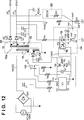
12 ist eine Schaltungsskizze, die ein Beispiel eines Schaltnetzteils mit zwei Ausgangsspannungen veranschaulicht. Gleiche Symbole und gleiche Bezugszeichen in 12 und 8 bezeichnen gleiche Komponenten. 12 Fig. 12 is a circuit diagram illustrating an example of a switching power supply having two output voltages. Same symbols and same reference numbers in 12 and 8th denote the same components.
Ein Hauptunterschied gegenüber der Schaltung nach 8 besteht darin, dass zwei Arten von Ausgangsspannungen Vo1 und Vo2 erzeugt werden.A major difference from the circuit after 8th is that two types of output voltages Vo1 and Vo2 are generated.
Beispielsweise entspricht die Ausgangsspannung Vo1 24 V Gleichspannung als Kopf-Treiberspannung, und die Ausgangsspannung Vo2 beträgt 32 V entsprechend einer Motor-Treiberspannung. Um diese zwei Typen von Ausgangsspannungen zu erzeugen, sind auf der Sekundärseite des Transformators T9 zwei Wicklungen 12 (n2: Anzahl der Windungen) und 12A (n3: Anzahl der Windungen) vorgesehen, so dass die Ausgangsspannung Vo1 an der Wicklung 12 (n2: Windungszahl) und die Ausgangsspannung Vo2 an der Wicklung 12a (n3: Windungszahl) gebildet wird. Man beachte, dass die Symbole Is1, Is2 den Ausgangsstrom der Wicklungen 12 bzw. 12a darstellen. Wie der Fachmann auf diesem Gebiet erkennt, können die Wicklungen 12 und 12a über einen Zwischenanzapfpunkt 51 konfiguriert sein (die Wicklungen 12 und 12a teilen einen gemeinsamen Stiftanschluss des Transformators), oder die jeweiligen Wicklungen können unabhängig gewickelt sein.For example, the output voltage Vo1 corresponds to 24 V DC as the head drive voltage, and the output voltage Vo2 is 32 V in accordance with a motor drive voltage. To produce these two types of output voltages, T9 has two windings on the secondary side of the transformer 12 (n2: number of turns) and 12A (n3: number of turns) provided so that the output voltage Vo1 at the winding 12 (n2: number of turns) and the output voltage Vo2 at the winding 12a (n3: number of turns) is formed. Note that the symbols Is1, Is2 are the output current of the windings 12 respectively. 12a represent. As those skilled in the art will appreciate, the windings can 12 and 12a via an intermediate tapping point 51 be configured (the windings 12 and 12a share a common pin terminal of the transformer), or the respective windings may be wound independently.
Als Gleichricht- und Glättungsschaltung hinter der zusätzlichen Wicklung 12a sind eine Diode D51 und ein Elektrolytkondensator C51 angeordnet. An den Eingangsanschluss (REF) des Shunt-Regler-ICs 3 ist eine Rückkopplung von der Ausgangsspannung Vo2 zusätzlich zu der von der Ausgangsspannung Vo1 gelegt. In diesem Fall wird die Rückkopplung von der Ausgangsspannung Vo1 durch eine Gleichstromkopplung über den Widerstand R6 erreicht, jedoch wird jene von der Ausgangsspannung Vo2 durch eine Wechselstromkopplung mittels eines Widerstands R51 und eines Kondensators C52 (eine gestrichelte Linie 52 in 12) erreicht.As a rectifying and smoothing circuit behind the additional winding 12a For example, a diode D51 and an electrolytic capacitor C51 are arranged. To the input terminal (REF) of the shunt regulator IC 3 is a feedback of the output voltage Vo2 in addition to that of the output voltage Vo1. In this case, the feedback from the output voltage Vo1 is achieved by a DC coupling through the resistor R6, but that of the output voltage Vo2 by an AC coupling by means of a resistor R51 and a capacitor C52 (a broken line 52 in 12 ) reached.
Dies deshalb, weil die Ausgangsspannung Vo1 als Treiberspannung für den Druckkopf verwendet wird, wie oben erläutert wurde, und somit eine hochgenaue Steuerung erforderlich ist, wohingegen die Ausgangsspannung Vo2 eine zum Treiben eines Gleichstrommotors oder dergleichen verwendete Spannung ist, bei der Schwankungen in einem gewissen Ausmaß toleriert werden. Was also die Ausgangsspannung Vo2 angeht, so wird die Rückkopplung mittels Wechselstromkopplung eingesetzt, um einen extremen Spannungsabfall zu dem Zeitpunkt zu vermeiden, zu dem vorübergehend ein starker Strom fließt (beispielsweise bei Aktivierung eines Motors). In anderen Worten: bei der beispielhaften Schaltung nach 12 hat die Rückkopplung der Ausgangsspannung Vo1 stets Priorität. Andererseits ist für die Ausgangsspannung Vo2 die Regelung gemäß einem Rückkopplungsfaktor nur für momentane starke Lastschwankungen mit einer CR-Zeitkonstanten des Widerstands R51 und des Kondensators C52 implementiert.This is because the output voltage Vo1 is used as the drive voltage for the printhead, as explained above, and thus highly accurate control is required, whereas the output voltage Vo2 is a voltage used for driving a DC motor or the like, in which variations to some extent be tolerated. So, as far as the output voltage Vo2 is concerned, the feedback is used by means of AC coupling to avoid an extreme voltage drop at the time when a strong current temporarily flows (for example, when an engine is activated). In other words, in the example circuit according to 12 the feedback of the output voltage Vo1 always has priority. On the other hand, for the output voltage Vo2, the feedback-factor control is implemented only for momentary large load fluctuations with a CR time constant of the resistor R51 and the capacitor C52.
Man beachte, dass die japanische Patent-Offenlegungsschrift 6-178537 als Beispiel für den einschlägigen Stand der Technik bezüglich einer Regelung eines Schaltnetzteils zur Verfügung steht, welches zwei Ausgangsspannungen erzeugt.Note that the Japanese Patent Laid-Open Publication 6-178537 as an example of the relevant prior art with respect to a regulation of a switching power supply is available, which generates two output voltages.
Die japanische Patent-Offenlegungsschrift 6-178537 zeigt ein Verfahren zum Auswählen einer Ausgangsspannung als Regel-Zielgröße nach Maßgabe jeweiliger Lastströme mehrerer Ausgangsspannungen. Nach der japanischen Patent-Offenlegungsschrift 6-178537 wird eine Ausgangsspannung mit einem höheren Laststrom zur Ausführung der Regelung ausgewählt.The Japanese Patent Laid-Open Publication 6-178537 shows a method of selecting an output voltage as a control target in accordance with respective load currents of a plurality of output voltages. After Japanese Patent Laid-Open Publication 6-178537 becomes an output voltage with selected a higher load current to perform the scheme.
Allerdings leidet die konventionelle, in 12 dargestellte Schaltung unter folgenden Problemen: Da die Rückkopplung der Ausgangsspannung Vo2 durch Wechselstromkopplung erfolgt, erhält selbst dann, wenn ein Druckkopfbetrieb in einer Ruhephase während beispielsweise eines Hochgeschwindigkeits-Druckmediumvorschubs eingestellt ist, die Rückkopplung der Druckkopf-Spannung Vo1 in unerwünschter Weise Priorität. Aus diesem Grund schwankt die Motortreiberspannung Vo2 stark, was abträglichen Einfluss auf die Motorregelung hat. In der Praxis ist eine Hochgeschwindigkeitsregelung von Motoren in einem Bereich implementiert, in welchem die Stabilität einer derartigen Regelung in der herkömmlichen Schaltung aufrecht erhalten bleibt.However, the conventional suffers in 12 as shown in the following problems: since the feedback of the output voltage Vo2 is performed by AC coupling, even if printhead operation is set in a quiescent phase during, for example, high-speed print medium feeding, the feedback of the printhead voltage Vo1 becomes undesirably priority. For this reason, the motor drive voltage Vo2 fluctuates greatly, which has a detrimental effect on the motor control. In practice, high-speed control of motors is implemented in a range in which the stability of such control is maintained in the conventional circuit.
Andererseits kann in der in 12 dargestellten Schaltung die Rückkopplung der Ausgangsspannung Vo2 entsprechend der Motortreiberspannung auch mittels Gleichstromkopplung so wie bei der Ausgangsspannung Vo1 realisiert werden. In diesem Fall muss eine Entscheidung über ein relatives Rückkopplungsfaktor-Verhältnis zwischen den jeweiligen Ausgangsgrößen getroffen werden. Wenn für die Ausgangsspannung Vo1 entsprechend der Druckkopfspannung ein hohes Verhältnis eingestellt ist, bleibt die Stabilität der Ausgangsspannung Vo1 erhalten. Allerdings werden bei einem Motorantrieb oder einem Anhaltevorgang Schwankungen, die durch Über- oder Unterschreitung der Motortreiberspannung Vo2 hervorgerufen werden, größer als im Fall der Wechselstromkopplung. Wird hingegen ein hoher Rückkopplungsfaktor für die Ausgangsspannung Vo2 eingestellt, so nehmen die Schwankungen der Druckkopfspannung Vo1 zu, was die Bildqualität deutlich beeinträchtigt.On the other hand, in the in 12 represented circuit, the feedback of the output voltage Vo2 according to the motor drive voltage and DC coupling can be realized as in the output voltage Vo1. In this case, a decision must be made about a relative feedback factor ratio between the respective outputs. When a high ratio is set for the output voltage Vo1 corresponding to the print head voltage, the stability of the output voltage Vo1 is maintained. However, in a motor drive or a stopping operation, fluctuations caused by exceeding or falling below the motor drive voltage Vo2 become greater than in the case of AC coupling. If, on the other hand, a high feedback factor is set for the output voltage Vo2, the fluctuations in the print head voltage Vo1 increase, which significantly affects the image quality.
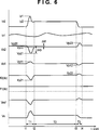
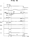
13 ist ein Wellenformdiagramm von Spannungs- und Stromwellenformen der jeweiligen Einheiten des in 12 dargestellten Schaltnetzteils für zwei Ausgangsspannungen. 13 is a waveform diagram of voltage and current waveforms of the respective units of the in 12 shown switching power supply for two output voltages.
Wenn zum Beispiel eine Aktivierungszeit (t = t1) des Transportmotors M2 betrachtet wird und ein Laststrom Io2 entsprechend der Motortreiberspannung von einem Spitzenstromwert Ip1 ausgehend reduziert wird, fällt die Ausgangsspannung Vo2 in diesem Zeitpunkt auf Vp21 ab (Unterschreitung). Ein Rückkopplungsstrom If2 (Wechselstrom) gemäß 13 fließt aus dem Knoten Vref1 zu der RC-Schaltung 52, und das Potential am Knoten Vref1 nimmt durch diesen abfließenden Strom ab.For example, when an activation time (t = t1) of the transport motor M2 is considered and a load current Io2 corresponding to the motor drive voltage is reduced from a peak current value Ip1, the output voltage Vo2 falls to Vp21 at this time (underflow). A feedback current If2 (AC) according to 13 flows from the node Vref1 to the RC circuit 52 , and the potential at the node Vref1 decreases by this outflowing current.
Im Ergebnis steigt die Ausgangsspannung Vk des Shunt-Regler-ICs 3 an, und die Einschaltzeit der PWM-Steuerung durch das Steuerungs-IC 1 nimmt zu, was zu einer Zunahme der von dem Transformator T9 erzeugten Energie führt und somit eine Regelung hervorruft, die die Ausgangsspannung Vo2 an einem Absinken hindert. Allerdings fällt in der in 12 dargestellten Schaltung im Anschluss an die Stabilisierung des Ausgangsstroms Io2 auf Ip2 im Zeitpunkt t = t2 die Ausgangsspannung Vo2 in unerwünschter Weise um ΔVf im Vergleich zu einem Pegel Vp20 vor dem Zeitpunkt t = t1 ab und nimmt einen Pegel Vp22 an.As a result, the output voltage Vk of the shunt regulator IC increases 3 on, and the on time of the PWM control by the control IC 1 increases, which leads to an increase in the energy generated by the transformer T9 and thus causes a control that prevents the output voltage Vo2 from falling. However falls in the in 12 shown circuit after the stabilization of the output current Io2 to Ip2 at the time t = t2, the output voltage Vo2 undesirably by ΔVf compared to a level Vp20 before the time t = t1 and assumes a level Vp22.
Dies deshalb, weil, wie aus der Schaltungsanordnung nach 12 ersichtlich ist, während einer stabilen Zeitspanne für die Ausgangsspannung Vo2 die Rückkopplung dieses Ausgangssignals aufgrund der Wechselstromkopplung nicht funktioniert und lediglich die Rückführung der Ausgangsgröße Vo1 wirklich wirksam ist. In anderen Worten: da die Rückkopplung der Ausgangsspannung Vo2 bezüglich Gleichstrom während der Zeitspanne T2 unkontrolliert ist, gibt es die Tendenz eines Spannungsabfalls bei einer Zunahme des Laststroms. Beispielsweise erreicht während einer Zeit, in der das Druckmedium mit Hochgeschwindigkeit durch den Transportmotor M2 in 11 transportiert wird, der Spannungsabfall ΔVf der Motor-Treiberspannung Vo2 einen Wert von etwa 3 bis 4 V.This is because, as in the circuit arrangement 12 can be seen, during a stable period for the output voltage Vo2, the feedback of this output signal due to the AC coupling does not work and only the return of the output Vo1 is really effective. In other words, since the feedback of the output voltage Vo2 with respect to DC during the period T2 is uncontrolled, there is a tendency of a voltage drop with an increase in the load current. For example, during a time when the printing medium reaches high speed through the transport motor M2 in FIG 11 is transported, the voltage drop .DELTA.Vf of the motor drive voltage Vo2 has a value of about 3 to 4 V.
Die Beschreibung wird unter erneuter Bezugnahme auf 13 fortgesetzt. Zu einem Zeitpunkt t = t3 wird der Treibervorgang für den Transportmotor M2 angehalten, und der Strom Io2 kehrt auf Null zurück. Die Ausgangsspannung Vo2 steigt dementsprechend sofort auf Vp23 an (Überschreitung), und der Rückkopplungsstrom If2 (Wechselstrom) fließt in umgekehrter Richtung von der RC-Schaltung 42 in den Knoten Vref1. Im Ergebnis steigt das Potential am Knoten Vref1 an, und die Ausgangsspannung Vk des Shunt-Regler-ICs 3 fällt ab, und die Einschaltzeit der PWM-Steuerung durch das Steuerungs-IC 1 nimmt ab, was die von dem Transformator T9 erzeugte Energie verringert. Auf diese Weise erfolgt die Regelung in der Weise, dass die Ausgangsspannung Vo2 an einem Ansteigen gehindert wird.The description will be made with reference to again 13 continued. At a time t = t3, the driving operation for the transport motor M2 is stopped, and the current Io2 returns to zero. Accordingly, the output voltage Vo2 immediately rises to Vp23 (overshoot), and the feedback current If2 (AC) flows in the reverse direction from the RC circuit 42 into the node Vref1. As a result, the potential at node Vref1 and the output voltage Vk of the shunt regulator IC increase 3 drops, and the on time of the PWM control by the control IC 1 decreases, which reduces the energy generated by the transformer T9. In this way, the control is performed in such a manner that the output voltage Vo2 is prevented from rising.
Man beachte, dass gemäß 13 die andere Ausgangsspannung Vo1 in den Zeitpunkten t = t1 und t3 beeinflusst wird und sich in einer Richtung entgegengesetzt zu der der Spannung Vo2 geringfügig ändert. Das heißt: zu Zeiten starker Schwankungen der Ausgangsspannung Vo2 zeigt der Ausgangsstrom Io1 der Ausgangsspannung Vo1 moderate Änderungen, wie aus 13 hervorgeht. Aus diesem Grund steigt aufgrund des Transfers hoher Energie von dem Transformator durch die Regelung aufgrund von Schwankungen der Ausgangsspannung Vo2 die Ausgangsspannung Vo1 zur Zeit t = t1 etwas an und erreicht einen Pegel Vp11, wie in 13 gezeigt ist. In ähnlicher Weise fällt im Zeitpunkt t = t3 die Ausgangsspannung Vo1 in entgegengesetzte Richtung auf einen Pegel von Vp12 etwas ab.Note that according to 13 the other output voltage Vo1 is influenced at times t = t1 and t3 and slightly changes in a direction opposite to that of the voltage Vo2. That is, at times of large fluctuations of the output voltage Vo2, the output current Io1 of the output voltage Vo1 shows moderate changes as shown 13 evident. For this reason, due to the high-energy transfer from the transformer due to the fluctuation of the output voltage Vo2, the output voltage Vo1 slightly increases at time t = t1 and reaches a level Vp11 as shown in FIG 13 is shown. Similarly, at time t = t3, the output voltage Vo1 slightly decreases in the opposite direction to a level of Vp12.
14 ist ein Blockdiagramm, welches die Regelanordnung für das in 12 dargestellte Schaltnetzteil für zwei Ausgangsspannungen veranschaulicht. Ein Unterschied gegenüber dem oben in Verbindung mit 9 beschriebenen Schaltnetzteil für eine Ausgangsspannung liegt darin, dass der Transformator 63 zwei Ausgänge (83a und 83b) aufweist, an den die beiden Ausgangsspannungen Vo1 und Vo2 über Gleichricht- und Glättungsschaltungen 84a bzw. 84b erzeugt werden, wie aus 14 hervorgeht. Außerdem werden einzelne Rückkopplungskomponenten aus den Ausgangssignalen Vo1 und Vo2 von einem Addierer 88 über Wichtungsschaltungen 86, 87 addiert, die Rückkopplungskomponenten entsprechend Rückkopplungsfaktoren α1 und α2 Wichten, und das Additionsergebnis wird von dem Fehlerverstärker 89 verarbeitet und schließlich zu der PWM-Steuereinheit 80 zurückgeführt. Damit erfährt der Treiber 82, der das Schaltelement (Q1) enthält, eine PWM-Steuerung und steuert damit eine von dem Transformator 83 zu erzeugende Energie. 14 is a block diagram illustrating the control arrangement for the in 12 illustrated switching power supply for two output voltages illustrated. A difference from the above in connection with 9 described switching power supply for an output voltage is that the transformer 63 two outputs ( 83a and 83b ) to which the two output voltages Vo1 and Vo2 via rectifying and smoothing circuits 84a respectively. 84b be generated as out 14 evident. In addition, individual feedback components from the output signals Vo1 and Vo2 from an adder 88 via weighting circuits 86 . 87 adds the feedback components corresponding to feedback factors α1 and α2, and the addition result is from the error amplifier 89 processed and finally to the PWM control unit 80 recycled. This tells the driver 82 , which includes the switching element (Q1), a PWM controller, thereby controlling one of the transformer 83 energy to be generated.
Insbesondere wird eine Änderung der Ausgangsspannung Vo1 über die Rückkopplung mit dem Rückkopplungsfaktor α1 wiedergespiegelt und eine Änderung der Ausgangsspannung Vo2 wird in der Regelung über den Rückkopplungsfaktor α2 wiedergespiegelt. Wie weiter unten erläutert wird, entsprechen diese Rückkopplungsfaktoren α1 und α2 den Graden oder Maßen des Beitrags der entsprechenden Ausgangsgrößen zu der Regelung.Specifically, a change of the output voltage Vo1 is reflected by the feedback with the feedback factor α1, and a change of the output voltage Vo2 is reflected in the feedback control by the feedback factor α2. As will be explained below, these feedback factors α1 and α2 correspond to the degrees of the contribution of the respective outputs to the control.
Die Beschreibung wird anhand der 12 und 14 fortgesetzt. Da die Rückkopplung der Ausgangsspannung Vo1 durch Gleichstromkopplung erfolgt, fließt der konstante Rückführstrom If1 (Gleichstrom) stets aus dem Ausgangsanschluss Vo1 zu dem Referenzanschluss Vref1 des Shunt-Reglers IC 3. Der Stromfluss If1 (Gleichstrom) ist gegeben durch: If(dc) = (Vo1 – Vref)/R6 (6) wobei die Referenzspannung Vref beispielsweise 2,5 V (DC) beträgt. Da andererseits die Rückkopplung der Ausgangsspannung Vo2 durch Wechselstromkopplung erfolgt, beträgt der Rückführstrom If2(ac), der von dem Ausgangsanschluss Vo2 zu dem Knoten Vref1 fließt, aufgrund der Sperrung durch den Kondensator C52 während einer stabilen Zeitspanne der Ausgangsspannung Vo2 Null. Deshalb ist die Gesamtsumme der Ströme, die in einer stabilen Zeitspanne von Vo2 in dem Knoten Vref1 einfließen, gegeben durch: If1(dc) + If2(ac) ≈ If1(dc) (∵If2(ac) ≈ 0) (7) The description is based on the 12 and 14 continued. Since the feedback of the output voltage Vo1 is done by DC coupling, the constant feedback current If1 (DC) always flows from the output terminal Vo1 to the reference terminal Vref1 of the shunt regulator IC 3 , The current flow If1 (DC) is given by: If (dc) = (Vo1 - Vref) / R6 (6) wherein the reference voltage Vref is 2.5 V (DC), for example. On the other hand, since the feedback of the output voltage Vo2 is performed by AC coupling, the feedback current If2 (ac) flowing from the output terminal Vo2 to the node Vref1 is zero due to the blocking by the capacitor C52 for a stable period of the output voltage Vo2. Therefore, the total sum of the currents flowing in a stable period of Vo2 in the node Vref1 is given by: If1 (dc) + If2 (ac) ≈If1 (dc) (∵If2 (ac) ≈ 0) (7)
Daher lautet der aus den Gleichungen (6) und (7) gewonnene Ausdruck (8) If1(dc) + If2(ac) ≈ (Vo1 – Vref)/R6 (8) Therefore, the expression obtained from equations (6) and (7) is (8) If1 (dc) + If2 (ac) ≈ (Vo1 - Vref) / R6 (8)
Außerdem werden aus der Gleichung (8) die Rückkopplungsfaktoren α1 und α2 folgendermaßen errechnet: α1 = 1/R6, α2 = 0 (9) In addition, from the equation (8), the feedback factors α1 and α2 are calculated as follows: α1 = 1 / R6, α2 = 0 (9)
Dies deshalb, weil dann, wenn die Ausgangsspannungen Vo1 und Vo2 als Variablen in der Gleichung (8) betrachtet werden, ihre Koeffizienten den Rückkopplungsfaktoren entsprechen. In der Praxis allerdings erscheint die Variable Vo2 in der Gleichung (8) nicht, und α2 wird Null.This is because, when the output voltages Vo1 and Vo2 are regarded as variables in the equation (8), their coefficients correspond to the feedback factors. In practice, however, the variable Vo2 does not appear in equation (8), and α2 becomes zero.
Als nächstes werden aus der Gleichung (9) Rückkopplungsbeitragsverhältnisse D(α1) und D(α2) für α1 bzw. α2 folgendermaßen berechnet: D(α1) = α1/(α1 + α2) = 1,0 (10) D(α2) = 0 (11) Next, from the equation (9), feedback contribution ratios D (α1) and D (α2) for α1 and α2 are calculated as follows: D (α1) = α1 / (α1 + α2) = 1.0 (10) D (α2) = 0 (11)
Wie aus der obigen Beschreibung ersichtlich ist, trägt lediglich die Ausgangsgröße Vo1 zu der Rückkopplung während einer stabilen Zeitspanne für die Ausgangsspannung Vo2 (die Zeitspanne T2 in 13) bei.As apparent from the above description, only the output Vo1 contributes to the feedback during a stable period for the output voltage Vo2 (the time T2 in FIG 13 ) at.
Andererseits ist gemäß 12 der Strom Iref1, der aus den Knoten Vref1 fließt, gegeben durch: Iref1 = Vref/R7 (12) On the other hand, according to 12 the current Iref1 flowing out of the nodes Vref1 given by: Iref1 = Vref / R7 (12)
Da der in dem Knoten Vref1 fließende Strom und der aus dem Knoten fließende Strom von dem Fehlerverstärker 14, der den Shunt-Regler IC 3 enthält, so geregelt werden, dass sie einander gleich sind, erhält man: If1(dc) + If2(ac) = Vref/R7 (13) Since the current flowing in the node Vref1 and the current flowing out of the node from the error amplifier 14 who has the shunt regulator IC 3 contains, be regulated so that they are equal to each other, one obtains: If1 (dc) + If2 (ac) = Vref / R7 (13)
In diesem Fall erhält man aus der Gleichung (7) die folgende Gleichung (14): If1(dc) ≈ Vref/R7 (14) In this case, from equation (7), the following equation (14) is obtained: If1 (dc) ≈Vref / R7 (14)
Wenn andererseits die Motortreiberspannung innerhalb der Zeitspanne T1 in 13 momentan schwankt (zum Beispiel zur Aktivierungszeit des Transportmotors M2 und des Schlittenmotors M1), reduziert sich die Ausgangsspannung Vo2 um eine Spannung, die zu einem großen Strom führt.On the other hand, if the motor drive voltage within the period T1 in 13 momentarily fluctuates (for example, the activation time of the transport motor M2 and the carriage motor M1), the output voltage Vo2 is reduced by a voltage that leads to a large current.
Wenn also die Rückkopplung der Ausgangsspannung Vo2 nicht berücksichtigt wird, bewirkt die Ausgangsspannung Vo2 zu diesem Zeitpunkt einen starken Spannungsabfall, und die Regelung der Motoren wird abnormal. Da die in 12 dargestellte Schaltung die Rückkopplung mittels der Wechselstromkopplung der Ausgangsspannung Vo2 ausführt, findet folglich die folgende Rückkopplungskorrektur gegenüber derartigen momentanen Schwankungen der Ausgangsspannung Vo2 statt. Das heißt, wenn ΔVp eine Spannungsschwankung der Ausgangsgröße Vo2 ist, fließt der Rückkopplungsstrom If2(ac) bezüglich der Ausgangsspannung Vo2 aus dem Knoten Vref1 zu der CR-Schaltung 52 (vgl. 12): If2(ac) = –ΔVp/R51·exp(–T/CR) (15) Thus, if the feedback of the output voltage Vo2 is disregarded, the output voltage Vo2 at this time causes a large voltage drop, and the control of the motors becomes abnormal. Since the in 12 shown circuit the feedback by means of AC coupling of the output voltage Vo2, thus takes place the following feedback correction against such instantaneous fluctuations of the output voltage Vo2. That is, when ΔVp is a voltage fluctuation of the output Vo2, the feedback current If2 (ac) flows from the node Vref1 to the CR circuit with respect to the output voltage Vo2 52 (see. 12 ): If2 (ac) = -ΔVp / R51 * exp (-T / CR) (15)
In diesem Fall bedeutet das Minuszeichen in der Gleichung (15), dass der Strom aus dem Knoten Vref1 herausfließt. Außerdem handelt es sich bei C der CR-Zeitkonstanten in der Gleichung (15) um einen Wert des Kondensators C52, R entspricht dem Widerstandswert des Widerstands R51, und die Variable T entspricht der verstrichenen Zeit im Anschluss an die Aktivierung des Motors, das heißt eine verstrichene Zeit im Anschluss an den Zeitpunkt t = t1 in 13. Darüber hinaus zeigt die Zeitspanne T1 für Vref1 gemäß 13 einen Potentialabfallzustand des Knotens Vref1 durch die abfließende Strommenge If2(ac). In 13 zeigt Ifp21 einen Minimumwert für den Stromfluss If2(ac) während des Zeitintervalls T1, und Ifp22 ist ein Maximumwert des Stroms If2(ac) während des Zeitintervalls T3. Ferner gehört in 13 ein Zeitintervall T1 zwischen den Zeitpunkten t = t1 bis t2 zu der CR-Zeitkonstanten in der Gleichung (15).In this case, the minus sign in the equation (15) means that the current flows out of the node Vref1. In addition, C of the CR time constant in the equation (15) is a value of the capacitor C52, R is the resistance value of the resistor R51, and the variable T is the elapsed time following activation of the motor, that is, one elapsed time following the time t = t1 in 13 , In addition, the time period T1 for Vref1 is shown in FIG 13 a potential drop state of the node Vref1 by the outflow current amount If2 (ac). In 13 Ifp21 indicates a minimum value for the current flow If2 (ac) during the time interval T1, and Ifp22 is a maximum value of the current If2 (ac) during the time interval T3. Furthermore belongs in 13 a time interval T1 between times t = t1 to t2 to the CR time constant in the equation (15).
Wie oben erläutert wurde, lässt sich für die Zeitspanne T1 in 13 aus den Gleichungen (6) und (15) eine Gesamtsumme der Rückkopplungsströme folgendermaßen berechnen: If1(dc) + If2(ac) = (Vo1 – Vref)/R6 – ΔVp/R51·exp(–T/CR) (16) As explained above, for the period T1 in FIG 13 from equations (6) and (15) calculate a total of the feedback currents as follows: If1 (dc) + If2 (ac) = (Vo1 -Vref) / R6 -ΔVp / R51 * exp (-T / CR) (16)
Aus der Gleichung (16) werden die jeweiligen Koeffizienten für die Variablen Vo1 und ΔVp, das heißt die Rückkopplungsfaktoren, wie folgt berechnet: α1 = 1/R6 (17) α2 = –1/R51·exp(–t/CR) (18) From the equation (16), the respective coefficients for the variables Vo1 and ΔVp, that is, the feedback factors, are calculated as follows: α1 = 1 / R6 (17) α2 = -1 / R51 * exp (-t / CR) (18)
In der Gleichung (18) bedeutet das Minuszeichen für α2 einen Abfall der Ausgangsspannung Vo2, ein Pluszeichen hingegen bedeutet einen Anstieg der Ausgangsspannung Vo2. Außerdem lässt sich aus der Gleichung (18) ersehen, dass der Rückkopplungsfaktor zu der Zeit t = 0 größer ist, wenn der Widerstand R51 in 12 kleiner wird.In the equation (18), the minus sign for α2 means a fall in the output voltage Vo2, while a plus sign means an increase in the output voltage Vo2. In addition, it can be seen from equation (18) that the feedback factor is greater at time t = 0 when resistor R51 in 12 gets smaller.
Dies bedeutet: der Strom, der aus dem Knoten Vref1 fließt, nimmt mit abnehmendem Widerstand R51 zu, und eine Änderung der Ausgangsspannung Vo2 spiegelt sich folglich mit hoher Empfindlichkeit an dem Knoten Vref1 wieder, wodurch die Änderung auf den nachfolgenden Fehlerverstärker 14 weitergeleitet wird. Wenn allerdings der Wert des Widerstands R51 auf einen sehr kleinen Wert eingestellt wird, wird der Einfluss des Rückkopplungsfaktors α2 zu groß und verursacht folglich ein Überschreiten oder Unterschreiten einer Rückkehrzeit von den Schwankungen der Ausgangsspannung Vo2, was die andere Ausgangsgröße Vo1 abträglich beeinflusst.That is, the current flowing from the node Vref1 increases with decreasing resistance R51, and a change of the output voltage Vo2 is consequently reflected with high sensitivity at the node Vref1, whereby the change to the subsequent error amplifier 14 is forwarded. However, if the value of the resistor R51 is set to a very small value, the influence of the feedback factor α2 becomes too large, and thus causes exceeding or falling below a return time from the fluctuations of the output voltage Vo2, which adversely affects the other output Vo1.
Wie außerdem aus der Gleichung (18) ersichtlich ist, enthält der Rückkopplungsfaktor für die Ausgangsgröße Vo2 eine Exponentialfunktion. Wenn also beispielsweise mehrere Motoren vorhanden sind (Schlittenmotor M1, Transportmotor M2, Scanner-Motor M3 und dergleichen), die unterschiedliche Aktivierungsströme haben, so ist es schwierig, sämtliche Motoren mit Hilfe eines Typs der CR-Zeitkonstanten optimal zu steuern.Also, as can be seen from equation (18), the feedback factor for the output Vo2 contains an exponential function. Thus, for example, if there are multiple motors (carriage motor M1, transport motor M2, scanner motor M3 and the like) having different activation currents, it is difficult to optimally control all the motors by means of one type of CR time constant.
Wie oben beschrieben wurde, wird bei dem in 12 gezeigten herkömmlichen Schaltnetzteil mit zwei Ausgangsspannungen ein optimaler Rückkopplungsfaktor für momentane Schwankungen der Motortreiberspannung, die durch Aktivierungszeitpunkte mehrerer Motoren verschiedener Aktivierungsströme hervorgerufen wird, nicht auswählbar sein. Darüber hinaus wird der Rückkopplungsfaktor α2 der Motortreiberspannung tatsächlich Null, nachdem die Motoren einen nahezu stabilisierten Zustand erreichen, was in der Folge einen Abfall dieser Ausgangsspannung verursacht. Im Ergebnis lässt sich in der in 12 dargestellten herkömmlichen Schaltung die Druckkopf-Treiberschaltung präziser aufrecht erhalten, wohingegen die Motortreiberspannung in unerwünschter Weise während eines Hochgeschwindigkeits-Druckträgertransports oder dergleichen unerwünscht abfällt. Folglich ist es schwierig, einen Durchsatz mit hoher Geschwindigkeit zu erzielen.As described above, in the 12 shown two-output voltage switching power supply, an optimal feedback factor for instantaneous fluctuations of the motor drive voltage, which is caused by activation times of multiple motors different activation currents, not be selectable. In addition, the feedback coefficient α2 of the motor drive voltage actually becomes zero after the motors reach a nearly stabilized state, thus causing a fall in this output voltage. The result is in the in 12 1, the motor drive voltage undesirably drops undesirably during high-speed print carrier transport or the like. As a result, it is difficult to achieve a high-speed throughput.
OFFENBARUNG DER ERFINDUNGDISCLOSURE OF THE INVENTION
Dementsprechend wurde die vorliegende Erfindung als Antwort auf die oben erläuterten Nachteile des Standes der Technik gemacht.Accordingly, the present invention has been made in response to the above-discussed disadvantages of the prior art.
Beispielsweise sind eine Stromversorgungsvorrichtung und eine Druckvorrichtung gemäß der Erfindung in der Lage, eine Druckkopf-Treiberspannung präzise zu steuern, während die erforderliche Stabilität für eine Motortreiberspannung entsprechend einem Druckvorgang erreicht wird.For example, a power supply device and a printing device according to the invention are capable of precisely controlling a printhead drive voltage while achieving the required stability for a motor drive voltage corresponding to a printing operation.
Gemäß einem Aspekt der Erfindung wird eine Stromversorgungsvorrichtung geschaffen, welche aufweist:
einen Transformator mit einer Primärwicklung, einer ersten Sekundärwicklung und einer zweiten Sekundärwicklung; eine erste Gleichspannungs-Erzeugungseinrichtung, konfiguriert zum Erzeugen einer ersten Gleichspannung aus einer von der ersten Sekundärwicklung erzeugten Spannung; eine zweite Gleichspannungs-Erzeugungseinrichtung, konfiguriert zum Erzeugen einer zweiten Gleichspannung aus einer Spannung, die erhalten wird durch Überlagern einer von der zweiten Sekundärwicklung erzeugten Spannung mit der ersten Gleichspannung; eine Schalteinrichtung, konfiguriert zum Erregen der Primärwicklung; und eine Steuereinrichtung mit einem Spannungseingangsknoten, konfiguriert zum Steuern der Schalteinrichtung in der Weise, dass eine an den Spannungseingangsknoten angelegte Spannung konstant wird, wobei der Spannungseingangsknoten mit einem Ausgangsknoten der ersten Gleichspannungs-Erzeugungseinrichtung, einem Ausgangsknoten der zweiten Gleichspannungs-Erzeugungseinrichtung und Masse jeweils über Widerstände verbunden ist.According to one aspect of the invention, there is provided a power supply apparatus comprising:
a transformer having a primary winding, a first secondary winding and a second secondary winding; a first DC voltage Generating means configured to generate a first DC voltage from a voltage generated by the first secondary winding; a second DC voltage generating device configured to generate a second DC voltage from a voltage obtained by superimposing a voltage generated by the second secondary winding on the first DC voltage; a switching device configured to energize the primary winding; and a controller having a voltage input node configured to control the switching device such that a voltage applied to the voltage input node becomes constant, the voltage input node having an output node of the first DC voltage generator, an output node of the second DC voltage generator, and ground via resistors, respectively connected is.
Gemäß einem weiteren Aspekt der Erfindung wird eine Druckvorrichtung mit einem Druckkopf und einem Motor geschaffen, wobei die Vorrichtung aufweist: eine geschaltete Stromversorgung, konfiguriert zum Erzeugen einer ersten Ausgangsspannung, die benötigt wird zum Treiben des Druckkopfs, und einer zweiten Ausgangsspannung, die höher als die erste Ausgangsspannung ist, erforderlich zum Treiben des Motors, und wobei die geschaltete Stromversorgung aufweist: einen Transformator, konfiguriert zum Erzeugen der ersten Ausgangsspannung durch eine erste Sekundärwicklung und zum Erzeugen einer Überlagerungsspannung zum Überlagern der ersten Ausgangsspannung durch eine zweite Sekundärwicklung; einen Treiber, konfiguriert zum Treiben des Transformators; eine erste Gleichricht- und Glättungsschaltung, konfiguriert zum Gleichrichten und Glätten der ersten Ausgangsspannung; eine zweite Gleichricht- und Glättungsschaltung, konfiguriert zum Gleichrichten und Glätten der Überlagerungsspannung; einen Addierer, konfiguriert zum Addieren der Überlagerungsspannung, die von der zweiten Gleichricht- und Glättungsschaltung gleichgerichtet und geglättet wurde, zu der ersten Ausgangsspannung, die von der ersten Gleichricht- und Glättungsschaltung gleichgerichtet und geglättet wurde, um die zweite Ausgangsspannung auszugeben; und eine Rückkopplungs-Steuerschaltung, konfiguriert zum Rückkoppeln der ersten Ausgangsspannung und der zweiten Ausgangsspannung durch Gleichstromkopplung, um die rückgekoppelte erste Ausgangsspannung und die rückgekoppelte zweite Ausgangsspannung durch einen ersten Rückkopplungsfaktor bzw. einen zweiten Rückkopplungsfaktor einzustellen und die jeweiligen eingestellten Rückkopplungskomponenten zu kombinieren und zu verstärken, und um auf den Treiber durch die kombinierten und verstärkten Rückkopplungskomponenten eine PWM-Steuerung anzuwenden.In accordance with another aspect of the invention, there is provided a printing apparatus including a printhead and a motor, the apparatus comprising: a switched power supply configured to generate a first output voltage needed to drive the printhead and a second output voltage higher than that a first output voltage required for driving the motor, and wherein the switched power supply comprises: a transformer configured to generate the first output voltage through a first secondary winding and to generate a superposition voltage for superimposing the first output voltage through a second secondary winding; a driver configured to drive the transformer; a first rectifying and smoothing circuit configured to rectify and smooth the first output voltage; a second rectifying and smoothing circuit configured to rectify and smooth the superposition voltage; an adder configured to add the superimposing voltage rectified and smoothed by the second rectifying and smoothing circuit to the first output voltage rectified and smoothed by the first rectifying and smoothing circuit to output the second output voltage; and a feedback control circuit configured to feed back the first output voltage and the second output voltage by DC coupling to adjust the feedback first output voltage and the feedback second output voltage by a first feedback factor and a second feedback factor and to combine and amplify the respective adjusted feedback components. and apply PWM control to the driver through the combined and amplified feedback components.
Die Erfindung ist besonders vorteilhaft, da Rückkopplungsfaktoren entsprechen den beiden Ausgangsspannungen, die von einem einzelnen Transformator erzeugt werden, bedarfsweise zwischen den beiden Ausgangsspannungen geändert werden können. Bei einem Druckvorgang können also die Rückkopplungsfaktoren der jeweiligen Ausgangsspannungen quantitativ gesteuert werden. Im Ergebnis lässt sich ein hochqualitatives Bild drucken, während der Durchsatz durch Beschleunigung des Transports des Druckmediums verbessert werden kann.The invention is particularly advantageous in that feedback factors corresponding to the two output voltages generated by a single transformer can be changed as needed between the two output voltages. In a printing process, therefore, the feedback factors of the respective output voltages can be controlled quantitatively. As a result, a high-quality image can be printed while the throughput can be improved by speeding up the transportation of the print medium.
Weitere Merkmale der vorliegenden Erfindung ergeben sich aus der nachfolgenden Beschreibung beispielhafter Ausführungsformen (unter Bezugnahme auf die beigefügten Zeichnungen).Further features of the present invention will become apparent from the following description of exemplary embodiments (with reference to the accompanying drawings).
KURZE BESCHREIBUNG DER ZEICHNUNGENBRIEF DESCRIPTION OF THE DRAWINGS
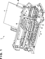
1 ist eine Schrägansicht, die eine Ausgestaltung einer Tintenstrahl-Druckvorrichtung als beispielhafte Ausführungsform der vorliegenden Erfindung veranschaulicht. 1 Fig. 10 is an oblique view illustrating an embodiment of an ink-jet printing apparatus as an exemplary embodiment of the present invention.
2 ist ein Blockdiagramm, das die Steueranordnung für die in 1 gezeigte Tintenstrahl-Druckvorrichtung veranschaulicht. 2 is a block diagram illustrating the control arrangement for the in 1 illustrated inkjet printing device illustrated.
3 ist ein Konzept-Diagramm einer Regelung eines Schaltnetzteils gemäß der vorliegenden Erfindung. 3 FIG. 10 is a conceptual diagram of a control of a switching power supply according to the present invention. FIG.
4 ist ein Schaltungsdiagramm des Schaltnetzteils gemäß der ersten Ausführungsform der Erfindung. 4 FIG. 12 is a circuit diagram of the switching power supply according to the first embodiment of the invention. FIG.
5 ist eine graphische Darstellung der Beziehung zwischen einem Parameter X und einem Rückkopplungs-Beitragsverhältnis. 5 Fig. 12 is a graph showing the relationship between a parameter X and a feedback contribution ratio.
6 ist ein Wellenformdiagramm, das Spannungs- und Stromwellenformen einzelner Einheiten der in 4 dargestellten Schaltung veranschaulicht. 6 is a waveform diagram showing voltage and current waveforms of individual units of the in 4 illustrated circuit illustrated.
7 ist eine Schaltungsskizze des Schaltnetzteils gemäß der zweiten Ausführungsform der Erfindung. 7 is a circuit diagram of the switching power supply according to the second embodiment of the invention.
8 ist eine Schaltungsskizze eines Beispiels für ein Schaltnetzteil, welches von einem herkömmlichen Sperrwandlerverfahren Gebrauch macht. 8th Fig. 12 is a circuit diagram of an example of a switching power supply which makes use of a conventional flyback converter method.
9 ist ein Blockdiagramm einer Ausgestaltung der Regelung des Schaltnetzteils nach 8. 9 is a block diagram of an embodiment of the control of the switching power supply according to 8th ,
10 ist ein Signalwellenformdiagramm von Spannungs- und Stromwellenformen einzelner Einheiten in dem in 8 gezeigten Schaltnetzteil. 10 FIG. 12 is a signal waveform diagram of voltage and current waveforms of individual units in the FIG 8th shown switching power supply.
11 ist ein Blockdiagramm der Ausgestaltung einer Stromversorgungseinheit für eine Tintenstrahl-Druckvorrichtung. 11 Fig. 10 is a block diagram of the configuration of a power supply unit for an ink-jet printing apparatus.
12 ist eine Schaltungsskizze eines Beispiels eines herkömmlichen Schaltnetzteils, das zwei Ausgangsspannungen erzeugt. 12 Fig. 12 is a circuit diagram of an example of a conventional switching power supply generating two output voltages.
13 ist ein Signalwellenform-Diagramm von Spannungs- und Stromwellenformen einzelner Einheiten in dem in 12 gezeigten Schaltnetzteil. 13 FIG. 12 is a signal waveform diagram of voltage and current waveforms of individual units in FIG 12 shown switching power supply.
14 ist ein Blockdiagramm einer Ausgestaltung einer Regelung des Schaltnetzteils nach 12. 14 is a block diagram of an embodiment of a regulation of the switching power supply according to 12 ,
15A und 15B sind anschauliche Schaltungsskizzen für einen Shunt-Regler. 15A and 15B are illustrative circuit sketches for a shunt regulator.
BESCHREIBUNG DER AUSFÜHRUNGSFORMDESCRIPTION OF THE EMBODIMENT
Anhand der begleitenden Zeichnungen wird im folgenden eine anschauliche Ausführungsform der vorliegenden Erfindung im einzelnen erläutert.Reference to the accompanying drawings, an illustrative embodiment of the present invention will be explained in detail below.
Im Rahmen der vorliegenden Beschreibung beinhalten die Begriffe „Druck” und ”Drucken” nicht nur die Erzeugung signifikanter Information wie zum Beispiel von Zeichen und graphischen Darstellungen, sondern beinhaltet in breitem Sinn die Erzeugung von Bildern, Figuren, Mustern und dergleichen auf einem Druckträger oder die Verarbeitung des Mediums ungeachtet, ob jene signifikant oder nicht signifikant sind, und ungeachtet, ob sie visualisiert sind, um von Menschen visuell wahrnehmbar zu sein.As used herein, the terms "printing" and "printing" include not only the generation of significant information such as characters and graphics, but broadly include the generation of images, figures, patterns, and the like on a print substrate or the like Processing the medium regardless of whether it is significant or not significant, and whether visualized to be visually perceptible by humans.
Außerdem beinhaltet der Begriff „Druckmedium” nicht nur einen Papierbogen, wie er in üblichen Druckern verwendet wird, sondern beinhaltet in breitem Sinn auch Materialien wie zum Beispiel Stoff, eine Kunststofffolie, eine Metallplatte, Glas, Keramik, Holz und Leder, die Tinte aufnehmen können.In addition, the term "print medium" not only includes a paper sheet as used in ordinary printers, but broadly includes materials such as cloth, a plastic film, a metal plate, glass, ceramics, wood, and leather that can hold ink ,
Außerdem sollte der Begriff „Tinte” (im folgenden auch als „Flüssigkeit” bezeichnet) in breitestem Sinn ähnlich der Definition des oben beschriebenen Begriffs „Druck” verstanden werden. Das heißt, „Tinte” beinhaltet auch eine Flüssigkeit, die bei Aufbringen auf einen Druckträger Bilder, Figuren, Muster und dergleichen erzeugen können, die den Druckträger verarbeiten kann, und die Tinte verarbeiten kann. Die Verarbeitung von Tinte beinhaltet zum Beispiel die Verfestigung oder die Unlösbarmachung eines Färbemittels, das in einer auf den Druckträger aufgebrachten Tinte enthalten ist.In addition, the term "ink" (hereinafter also referred to as "liquid") should be understood in a broad sense similar to the definition of the term "pressure" described above. That is, "ink" also includes a liquid that, when applied to a print substrate, can produce images, figures, patterns, and the like that can handle the print substrate and process the ink. The processing of ink includes, for example, solidification or insolubilization of a colorant contained in an ink applied to the print carrier.
Außerdem repräsentiert der Begriff „Druckelement” (auch als „Düse” bezeichnet) grundlegend eine Tintenöffnung, einen Tintenkanal, der mit dieser Öffnung kommuniziert, und ein Element, das erforderlich ist, um eine Energie zu erzeugen, die dazu dient, eine Tinte auszustoßen, wenn nichts anderes gesagt ist.In addition, the term "pressure element" (also referred to as "nozzle") basically represents an ink port, an ink channel communicating with that port, and an element required to generate energy used to eject an ink. unless otherwise stated.
<Ausgestaltung der Druckvorrichtung (Fig. 1 und Fig. 2)><Configuration of the Printing Device (FIGS. 1 and 2)>
1 ist eine Schrägansicht einer Anordnung einer Druckvorrichtung, die einen Druckvorgang unter Verwendung eines Tintenstrahl-Druckkopfs (im folgenden als Druckkopf bezeichnet) als beispielhafte Ausführungsform der vorliegenden Erfindung ausführt. 1 Fig. 11 is an oblique view of an arrangement of a printing apparatus which performs a printing operation using an ink-jet printhead (hereinafter referred to as a printhead) as an exemplary embodiment of the present invention.
Wie in 1 gezeigt ist, trägt eine Tintenstrahl-Druckvorrichtung (im folgenden als Druckvorrichtung bezeichnet) 1 einen Tintenstrahl-Druckkopf (im folgenden als Druckkopf bezeichnet) 3, der einen Druckvorgang dadurch ausführt, dass er eine Tinte entsprechend einem Tintenstrahl-Druckverfahren ausstößt und sich auf einem Schlitten 2 befindet, wobei der Schlitten 2 in Richtungen des Doppelpfeils A hin und her abtastend bewegt wird um auf diese Weise einen Druckvorgang auszuführen. Die Vorrichtung 1 führt über einen Papierzuführmechanismus 5 einen Druckträger P, beispielsweise einen Druckpapierbogen, einer Druckstelle zu und stößt Tinte auf den Druckträger P aus dem Druckkopf 3 aus, um dadurch den Druckvorgang zu bewerkstelligen.As in 1 is shown carrying an ink jet printing apparatus (hereinafter referred to as printing apparatus) 1 an ink-jet printhead (hereinafter referred to as a printhead) 3 which performs a printing operation by ejecting an ink according to an ink-jet printing method and on a carriage 2 is located, with the carriage 2 is scanned back and forth in directions of the double arrow A to perform a printing operation in this way. The device 1 leads through a paper feed mechanism 5 a print carrier P, for example, a printing paper sheet, a printing location and pushes ink on the print carrier P from the print head 3 to accomplish the printing process.
An dem Schlitten 2 der Druckvorrichtung 1 ist nicht nur der Druckkopf 3 angebracht, sondern an ihm sind auch Tintenbehälter 6 gelagert, die Tinten beinhalten, die dem Druckkopf 3 zuzuführen sind. Die Tintenbehälter 6 sind von dem Schlitten 2 abnehmbar.On the sledge 2 the printing device 1 is not just the printhead 3 attached, but on it are also ink tank 6 stored, which contain inks that the printhead 3 are to be supplied. The ink tanks 6 are from the sled 2 removable.
Die in 1 gezeigte Druckvorrichtung 1 ist in der Lage, einen Farbdruck auszuführen, wozu an dem Schlitten 2 vier Tintenpatronen angebracht sind, die jeweils Tinten der Farben Magenta (M), Cyan (C), Gelb (Y) und Schwarz (K) beinhalten. Diese vier Tintenpatronen sind unabhängig voneinander abnehmbar.In the 1 shown printing device 1 is able to perform a color print, including on the carriage 2 four ink cartridges are attached, each containing inks of the colors magenta (M), cyan (C), yellow (Y) and black (K). These four ink cartridges are independently removable.
Der Druckkopf 3 dieser Ausführungsform macht von einem Tintenstrahl-Druckverfahren Gebrauch, welches eine Tinte mit Hilfe von Wärmeenergie ausstößt. Zu diesem Zweck enthält der Druckkopf 3 elektrothermische Wandler. Die elektrothermischen Wandler sind entsprechend zugehörigen Öffnungen angeordnet, und Tinten werden aus den entsprechenden Öffnungen dadurch ausgestoßen, dass impulsförmige Spannungen an die entsprechenden elektrothermischen Wandler nach Maßgabe eines Drucksignals angelegt werden. Man beachte, dass die Druckvorrichtung nicht auf den oben erläuterten seriellen Druckertyp beschränkt ist, sondern dass die Erfindung auch bei einem sogenannten Vollzeilendrucker anwendbar ist, bei dem ein Druckkopf (Zeilenkopf) in Transportrichtung des Druckträgers angeordnet ist, wobei an den Druckkopf Öffnungen in Breitenrichtung eines Druckträgers angeordnet sind.The printhead 3 This embodiment makes use of an ink-jet printing method which ejects an ink by means of heat energy. For this purpose, the printhead contains 3 electrothermal transducers. The electrothermal transducers are disposed corresponding to respective openings, and inks are ejected from the respective openings by applying pulse-shaped voltages to the respective electrothermal transducers in accordance with a pressure signal. Note that the printing apparatus is not limited to the above-mentioned serial printer type, but that the invention is also applicable to a so-called full-line printer in which a print head (line head) is arranged in the transport direction of the print carrier, wherein openings are arranged in the width direction of a print carrier to the print head.
2 ist ein Blockdiagramm, welches die Steueranordnung für die in 1 gezeigte Druckvorrichtung veranschaulicht, 2 is a block diagram illustrating the control arrangement for the in 1 illustrated printing device illustrates
Wie in 2 gezeigt ist, enthält eine Steuerung 600 eine MPU 601, einen ROM 602, eine ASIC (anwendungsspezifische integrierte Schaltung) 603, einen RAM 604, einen Systembus 605, einen A/D-Wandler 606 und dergleichen. Der ROM 602 speichert ein Programm entsprechend einer Steuersequenz (die weiter unten zu beschreiben ist), benötigte Tabellen und weitere permanente Daten. Die ASIC 603 generiert Steuersignale zum Steuern eines Schlittenmotors M1, eines Transportmotors M2 und des Druckkopfs 3. Der RAM 604 dient als Erweiterungsbereich für Bilddaten, als Arbeitsbereich zum Ausführen eines Programms und dergleichen. Der Systembus 605 verbindet die MPU 601, die ASIC 603 und den RAM 604 miteinander zum Austausch von Daten. Der A/D-Wandler 606 empfängt Analogsignale von (noch zu beschreibenden) Sensoren, unterzieht diese Signale einer A/D-Umsetzung und liefert digitale Signale an die MPU 601.As in 2 is shown contains a controller 600 an MPU 601 , a ROM 602 , an ASIC (application specific integrated circuit) 603 , a ram 604 , a system bus 605 , an A / D converter 606 and the same. The ROM 602 stores a program according to a control sequence (to be described below), required tables and other permanent data. The ASIC 603 generates control signals for controlling a carriage motor M1, a transport motor M2 and the print head 3 , The RAM 604 serves as an expansion area for image data, a work area for executing a program and the like. The system bus 605 connects the MPU 601 , the ASIC 603 and the RAM 604 together to exchange data. The A / D converter 606 receives analog signals from sensors (to be described), subjects these signals to A / D conversion and provides digital signals to the MPU 601 ,
In 2 bezeichnet das Bezugszeichen 610 eine Host-Vorrichtung, die als Bilddaten-Lieferquelle dient und einer Host-Vorrichtung wie beispielsweise einem Personal-Computer, einer Digitalkamera, einem Scanner, einem Speicherstick oder dergleichen entspricht. Die Host-Vorrichtung 610 und die Druckvorrichtung 1 tauschen Bilddaten, Befehle, Statusmeldungen und dergleichen unter Verwendung von Paket-Kommunikationen über eine Schnittstelle (I/F) 611 aus. Man beachte, dass eine USB-Schnittstelle zusätzlich unabhängig von einer Netzwerkschnittstelle als Schnittstelle 611 vorhanden sein kann, um bitweise Daten und Rasterdaten empfangen zu können, die seriell von dem Host übertragen werden.In 2 denotes the reference numeral 610 a host device serving as an image data supply source and corresponding to a host device such as a personal computer, a digital camera, a scanner, a memory stick, or the like. The host device 610 and the printing device 1 exchange image data, commands, status messages and the like using packet communications via an interface (I / F) 611 out. Note that a USB interface is also independent of a network interface as an interface 611 may be present to receive bitwise data and raster data transmitted serially by the host.
Weiterhin bezeichnet das Bezugszeichen 620 Schalter, darunter einen Netzschalter 621, einen Druckschalter 622, einen Recovery-Schalter 623 und dergleichen.Furthermore, the reference numeral designates 620 Switch, including a power switch 621 , a pressure switch 622 , a recovery switch 623 and the same.
Bezugszeichen 630 bezeichnet Sensoren, die dazu dienen, Apparaturzustände nachzuweisen, sie enthalten einen Stellungssensor 631, einen Temperatursensor 632 und dergleichen. Bei dieser Ausführungsform sind zusätzlich zu den genannten Sensoren Photosensoren vorhanden, die Tinten-Restmengen ermitteln.reference numeral 630 indicates sensors that serve to detect equipment conditions, they contain a position sensor 631 , a temperature sensor 632 and the same. In this embodiment, in addition to the above-mentioned sensors, photosensors exist which detect residual amounts of ink.
Bezugszeichen 640 bezeichnet einen Schlittenmotortreiber, der erforderlich ist, um den Schlittenmotor M1 zum Hin- und Herbewegen des Schlittens 2 in Richtung des Doppelpfeils A zu treiben, 642 bezeichnet einen Transportmotortreiber, der dazu dient, den Transportmotor M2 zu treiben, damit dieser das Druckmedium P transportiert.reference numeral 640 denotes a carriage motor driver required to move the carriage motor M1 to reciprocate the carriage 2 in the direction of the double arrow A, 642 denotes a transport motor driver which serves to drive the transport motor M2 to convey the printing medium P.
Die ASIC 603 überträgt Daten zum Treiben von Druckelementen (Ausstoß-Heizvorrichtungen) an den Druckkopf unter direktem Zugriff auf einen Speicherbereich des RAM 604 bei Ausführung von Druck-Abtastvorgängen durch den Druckkopf 3. Darüber hinaus enthält diese Druckvorrichtung eine Anzeigeeinheit, konfiguriert mittels LCD und LEDs in Form einer Benutzerschnittstelle.The ASIC 603 transfers data for driving printing elements (ejection heaters) to the print head with direct access to a memory area of the RAM 604 when performing print scans by the printhead 3 , Moreover, this printing device includes a display unit configured by means of LCD and LEDs in the form of a user interface.
Ein Schaltnetzteil, das elektrische Energie an die einzelnen Einheiten der Druckvorrichtung mit der obigen Ausgestaltung liefert, wird im folgenden beschrieben.A switching power supply that supplies electric power to the individual units of the printing apparatus having the above configuration will be described below.
3 ist ein Blockdiagramm, welches die Regelungsanordnung eines Schaltnetzteils veranschaulicht, welches zwei Ausgangsspannungen (zum Erzeugen zweier verschiedener Spannungen) enthält. Gleiche Bezugszeichen und Symbole in 3 bezeichnen gleiche Elemente und Signale, die oben in Verbindung mit dem in 14 gezeigten herkömmlichen Schaltnetzteil erläutert wurden, auf eine Wiederholung der Beschreibung wird verzichtet. In diesem Zusammenhang wird eine Gleichricht- und Glättungsschaltung 84a als erste Gleichricht- und Glättungsschaltung bezeichnet, eine Gleichricht- und Glättungsschaltung 84b wird im folgenden als zweite Gleichricht- und Glättungsschaltung bezeichnet. 3 Figure 4 is a block diagram illustrating the control arrangement of a switched-mode power supply which includes two output voltages (for generating two different voltages). Same reference numerals and symbols in 3 denote the same elements and signals as described above in connection with FIG 14 have been explained, a repetition of the description will be omitted. In this context, a rectifying and smoothing circuit 84a referred to as a first rectifying and smoothing circuit, a rectifying and smoothing circuit 84b is referred to as a second rectifying and smoothing circuit hereinafter.
Haupt-Unterschiede gegenüber der in 14 gezeigten herkömmlichen Ausgestaltung beinhalten die folgenden drei Punkte:
- (1) eine Motortreiberspannung Vo2 wird erzeugt durch Überlagern einer Spannung bezüglich einer Druckkopf-Treiberspannung Vo1 unter Bezug auf die Druckkopf-Treiberspannung Vo1;
- (2) beide Ausgangsspannungen Vo1 und Vo2 werden durch Gleichstromkopplung zurückgeführt; und
- (3) Rückkopplungsfaktoren α1 und α2 der Ausgangsspannungen Vo1 und Vo2 sind relativ zueinander variabel steuerbar.
Main differences over in 14 The conventional embodiment shown includes the following three points: - (1) a motor drive voltage Vo2 is generated by superimposing a voltage with respect to a printhead drive voltage Vo1 with reference to the printhead drive voltage Vo1;
- (2) both output voltages Vo1 and Vo2 are fed back through DC coupling; and
- (3) Feedback factors α1 and α2 of the output voltages Vo1 and Vo2 are variably controllable relative to each other.
Mit dieser Ausgestaltung wird eine zweite Ausgangsspannung Vo2 folgendermaßen generiert: Vo2 = Vo1 + ΔVs (19) wobei Vo1 eine erste Ausgangsspannung, ΔVs eine der Ausgangsspannung Vo1 zu überlagernde Spannung und Vo2 die zweite Ausgangsspannung ist. Wie aus 3 ersichtlich ist, addiert ein Addierer 803 die zu überlagernde Spannung ΔVs der ersten Ausgangsspannung Vo1, um dadurch die zweite Ausgangsspannung Vo2 zu erzeugen.With this embodiment, a second output voltage Vo2 is generated as follows: Vo2 = Vo1 + ΔVs (19) where Vo1 is a first output voltage, ΔVs is a voltage to be superimposed on the output voltage Vo1, and Vo2 is the second output voltage. How out 3 is apparent, adds an adder 803 the superimposed voltage .DELTA.Vs of the first output voltage Vo1 to thereby generate the second output voltage Vo2.
Wenn also die Ausgangsspannung Vo1 stabil geregelt wird, hängen Schwankungen der Ausgangsgröße Vo2 nur von der überlagernden Spannung ΔVs ab. In anderen Worten: da die Stabilität der Ausgangsspannung Vo2 von derjenigen der Ausgangsspannung Vo1 abhängt, wird, wenn die Stabilität von Vo1 in zufriedenstellender Weise aufrecht erhalten wird und die überlagernde Spannung ΔVs stabil gehalten wird, das heißt, wenn eine konstante Rückkopplung zu der überlagernden Spannung ΔVs erfolgt, kann auch die Ausgangsspannung Vo2 stabil geregelt werden.Thus, when the output voltage Vo1 is stably controlled, variations in the output Vo2 depend only on the superposed voltage ΔVs. In other words, since the stability of the output voltage Vo2 depends on that of the output voltage Vo1, if the stability of Vo1 is satisfactorily maintained and the superimposed voltage ΔVs is kept stable, that is, if there is a constant feedback to the superimposed voltage ΔVs, the output voltage Vo2 can be stably controlled.
Man beachte, dass in 3 ein Rückkopplungsfaktor der Ausgangsgröße Vo1 den Wert α1 hat, derjenige der Ausgangsgröße Vo2 hat den Wert α2. In diesem Fall wird α1 im folgenden als ein erster Rückkopplungsfaktor und α2 als ein zweiter Rückkopplungsfaktor bezeichnet. Mit diesen Faktoren werden Rückkopplungs-Anteilsverhältnisse der Ausgangsspannungen Vo1 und Vo2 eingestellt. Ein Addierer 88 addiert jeweilige Rückkopplungskomponenten, und das Ergebnis wird in einen Fehlerverstärker 89 eingegeben und verstärkt. Schließlich unterzieht eine PWM-Steuereinheit 80 einen Treiber 82, der ein Schaltelement (Q1) enthält, einer PWM-Steuerung, um dadurch die von einem Transformator 83 zu erzeugende Energie zu steuern. Im Ergebnis wird eine Regelung der jeweiligen Ausgangsgrößen nach Maßgabe der Rückkopplungsfaktoren implementiert. Das heißt: mit der Ausgestaltung nach 3, das heißt dem Treiber 82 als Schalteinheit zum Erregen einer Primärwicklung des Transformators konfigurieren die PWM-Steuereinheit 80 und der Fehlerverstärker 89 eine Steuereinheit, welche die Schalteinheit steuert. Man beachte, dass die Ausgestaltung der PWM-Steuerung oben bereits anhand der 8 bis 10 erläutert wurde.Note that in 3 a feedback factor of the output Vo1 has the value α1, that of the output Vo2 has the value α2. In this case, α1 is hereinafter referred to as a first feedback factor and α2 as a second feedback factor. With these factors, feedback ratios of the output voltages Vo1 and Vo2 are adjusted. An adder 88 adds respective feedback components, and the result becomes an error amplifier 89 entered and strengthened. Finally undergoes a PWM control unit 80 a driver 82 comprising a switching element (Q1), a PWM control, thereby by a transformer 83 to control energy to be generated. As a result, a regulation of the respective output variables is implemented in accordance with the feedback factors. That is: with the design after 3 that is the driver 82 As a switching unit for energizing a primary winding of the transformer, configure the PWM control unit 80 and the error amplifier 89 a control unit which controls the switching unit. It should be noted that the design of the PWM control above already based on the 8th to 10 was explained.
Außerdem werden in der in 3 dargestellten Ausgestaltung die Rückkopplungsfaktoren α1 und α2 optional basierend auf einem Steuersignal (Cont) nach Maßgabe einer Druckablauffolge der Druckvorrichtung gesteuert. Insbesondere werden, wie weiter unten noch erläutert wird, die jeweiligen Rückkopplungsfaktoren derart ausgewählt, dass die Druckkopf-Treiberschaltung Vo1 während einer Druckphase vorzugsweise gesteuert wird, dabei werden sie aber so ausgewählt, dass Schwankungen der Motortreiberspannung Vo2 beim Transport eines Druckmediums unterdrückt werden.In addition, in the in 3 illustrated embodiment, the feedback factors α1 and α2 optionally controlled based on a control signal (Cont) in accordance with a print sequence of the printing device. Specifically, as will be explained later, the respective feedback factors are selected such that the printhead driver circuit Vo1 is preferentially controlled during a printing phase, but are selected so as to suppress variations in the motor drive voltage Vo2 during transport of a printing medium.
4 ist eine Schaltungsskizze, die die Ausgestaltung eines die Regelung nach 3 implementierenden Schaltnetzteils mit zwei Ausgangsspannungen veranschaulicht. Man beachte, dass eine Schaltung mit einer Diode D2 und einem Kondensator C4 eine erste Gleichspannungs-Erzeugungsschaltung bildet. Eine Schaltung mit einer Diode D91 und einem Kondensator C91 ist eine zweite Gleichspannungs-Erzeugungsschaltung. Eine Entsprechung zwischen der Anordnung nach 3 und der nach 4 wird erläutert. Ein Schaltelement Q1 in 4 ist in dem in 3 gezeigten Treiber 82 enthalten. Ein Steuerungs-IC 1 in 3 ist in der in 3 gezeigten PWM-Steuereinheit 80 enthalten. Eine Steuerschaltung 14 nach 4 ist in dem Fehlerverstärker 89 enthalten. 4 is a circuit diagram showing the design of the scheme after 3 implementing switching power supply with two output voltages illustrated. Note that a circuit having a diode D2 and a capacitor C4 constitutes a first DC voltage generating circuit. A circuit having a diode D91 and a capacitor C91 is a second DC voltage generating circuit. A correspondence between the arrangement 3 and the after 4 will be explained. A switching element Q1 in 4 is in the in 3 shown driver 82 contain. A control IC 1 in 3 is in the in 3 shown PWM control unit 80 contain. A control circuit 14 to 4 is in the error amplifier 89 contain.
Man beachte, dass gleiche Bezugszeichen und Symbole in 4 für gleiche Elemente und Signale stehen, wie sie oben in Verbindung mit dem in 12 gezeigten Schaltnetzteil erläutert wurden, so dass auf eine nochmalige Beschreibung verzichtet wird. Wie aus einem Vergleich zwischen den 4 und 12 ersichtlich ist, liegen die Unterschiede gegenüber der in 12 dargestellten herkömmlichen Schaltung in folgenden Punkten: erste und zweite Wicklungen 12 (n2: Windungszahl) und 12a (n3: Windungszahl) eines Transformators T9 sind unabhängig ohne irgendeinen Zwischenanzapfpunkt angeordnet, eine Ausgangswicklung 12a ist so verschaltet, dass sie als Ursprung einen Knoten 91 aufweist, bei dem die Ausgangsspannung Vo1 gleichgerichtet und geglättet ist, während die Ausgangsspannung Vo2 über die Diode D91 und den Kondensator C91 der Gleichricht- und Glättungsschaltung erzeugt wird.Note that like reference numerals and symbols in FIG 4 stand for the same elements and signals, as mentioned above in connection with the in 12 have been explained switching power supply, so that dispenses with a repeated description. As if from a comparison between the 4 and 12 can be seen, the differences are different from those in 12 illustrated conventional circuit in the following points: first and second windings 12 (n2: number of turns) and 12a (n3: number of turns) of a transformer T9 are arranged independently without any intermediate tap point, an output winding 12a is connected so that it has a node as the origin 91 in which the output voltage Vo1 is rectified and smoothed while the output voltage Vo2 is generated across the diode D91 and the capacitor C91 of the rectifying and smoothing circuit.
Da bei dieser Anordnung die Ausgangsspannung Vo2 erzeugt wird, während sie der stabilen Ausgangsspannung (der ersten Gleichspannung) Vo1 überlagert ist, kann die Ausgangsspannung (die zweite Gleichspannung) Vo2 folglich von der Stabilisierung der Ausgangsspannung Vo1 profitieren. Im Ergebnis lässt sich im Vergleich zu der in 12 gezeigten Schaltung eine stabilere Ausgangsspannung Vo2 erreichen. Da außerdem bei dieser Ausführungsform die beiden Ausgangsgrößen Vo1 und Vo2 eine Rückregelung mittels Gleichstromkopplung aufweisen, kann die Ausgangsgröße Vo2 im Vergleich zu der in 12 gezeigten herkömmlichen Schaltung quantitativ stabilisiert werden.With this arrangement, since the output voltage Vo2 is generated while being superposed on the stable output voltage (the first DC voltage) Vo1, the output voltage (the second DC voltage) Vo2 can thus profit from the stabilization of the output voltage Vo1. As a result, compared to the in 12 shown circuit achieve a more stable output voltage Vo2. In addition, in this embodiment, since the two outputs Vo1 and Vo2 have DC feedback feedback, the output Vo2 can be compared to that in FIG 12 shown in the conventional circuit can be quantitatively stabilized.
Als weiterer Vorteil ist zu nennen, dass eine tolerierbare Spannung der Gleichrichterdiode D91 weniger restriktiv ist im Vergleich zu der für die Diode D51 in 12, da eine für die Gleichrichterdiode geforderte Spitzen-Sperrspannung VRM kleiner ist.Another advantage is that a tolerable voltage of the rectifier diode D91 is less restrictive compared to that for the diode D51 in 12 because a peak reverse voltage VRM required for the rectifier diode is smaller.
Das heißt, in der in 12 gezeigten herkömmlichen Schaltung ist die Spitzen-Sperrspannung gegeben durch: VRm = Vin(dc)·(n2 + n3)/n1 + Vo2 + Vr (20) That is, in the in 12 As shown in the conventional circuit, the peak reverse voltage is given by: VRm = Vin (dc) * (n2 + n3) / n1 + Vo2 + Vr (20)
Im Gegensatz dazu ist bei der vorliegenden Ausführungsform die Spitzen-Sperrspannung VRm gegeben durch: VRm = Vin(dc)·n3/n1 + Vo2 + Vr (21) In contrast, in the present embodiment, the peak reverse voltage VRm is given by: VRm = Vin (dc) * n3 / n1 + Vo2 + Vr (21)
Ein Vergleich der beiden Gleichungen ergibt, dass dann, wenn Terme von den Wicklungsverhältnissen des Transformators abhängen, das heißt, wenn man die ersten Terme der Gleichungen (20) und (21) vergleicht, ein Faktor der primären geglätteten Gleichspannung Vin(dc) (n2 + n3)/n1 in der Gleichung (20) ist, in der Gleichung (21) hingegen n3/n1. Das heißt: im letzteren Fall ist ein kleinerer Wert angenommen, und dementsprechend ist die Spitzen-Sperrspannung VRm verringert. Man beachte, dass in den Gleichungen (20) und (21) die primäre geglättete Gleichspannung Vin(dc) eine Gleichspannung ist als Ergebnis der Gleichrichtung und Glättung der Eingangsspannung von 100 V bis 240 V Wechselstrom, und Vr eine Stoßspannung ist, verursacht durch eine Streuinduktivität in Bezug auf die Sekundärwicklungen 12 (Windungszahl n2) und 12a (Windungszahl n3) des Transformators T9. In diesem Fall wird die Wicklung 12 im folgenden als erste Sekundärwicklung, die Wicklung 12a als zweite Sekundärwicklung bezeichnet.A comparison of the two equations reveals that when terms depend on the winding ratios of the transformer, that is, comparing the first terms of equations (20) and (21), a factor of the primary smoothed DC voltage Vin (dc) (n2 + n3) / n1 in the equation (20), in the equation (21), however, n3 / n1. That is, in the latter case, a smaller value is assumed and, accordingly, the peak withstand voltage VRm is reduced. Note that in equations (20) and (21), the primary DC smoothed voltage Vin (dc) is a DC voltage as a result of the rectification and smoothing of the input voltage of 100V to 240VAC, and Vr is a surge voltage caused by a Leakage inductance with respect to the secondary windings 12 (Number of turns n2) and 12a (Number of turns n3) of the transformer T9. In this case, the winding becomes 12 in the following as the first secondary winding, the winding 12a referred to as second secondary winding.
Wenn zum Beispiel Vo1 = DC 24 V und Vo2 = DC 32 V betragen, so erfordert die Spitzen-Sperrspannung VRm der Diode D51 in der in 12 gezeigten herkömmlichen Schaltung eine Spannung von 200 V bis 250 V, allerdings reicht in der Schaltung dieser Ausführungsform nach 4 eine Spannung von VRm der Diode D91 von etwa 60 V.For example, if Vo1 = 24 V DC and Vo2 = 32 V DC, then the peak reverse voltage VRm requires the diode D51 in the in 12 A voltage of 200 V to 250 V shown in the conventional circuit shown, however, in the circuit of this embodiment is sufficient 4 a voltage of VRm of the diode D91 of about 60 V.
Die Beschreibung wird erneut in Bezug auf 4 aufgenommen. Die Steuerschaltung 14 besitzt einen Eingangsknoten 14 in und einen Ausgangsknoten 14 out. Der Eingangsknoten 14 in ist mit einem Anschluss jedes der Widerstände R6, R91 und R7 verbunden. Der andere Anschluss des Widerstands R6 ist mit einem Knoten 91 verbunden. Der andere Anschluss des Widerstands R91 ist mit einem Knoten 92 verbunden. Der andere Anschluss des Widerstands R7 ist mit Masse verbunden. Der Eingangsknoten 14 in ist mit einem Anschluss REF eines Shunt-Reglers IC 3 verbunden. Ein Ausgangsknoten 14 out ist mit einem Anschluss FB eines ICs 1 verbunden.The description will be repeated in relation to 4 added. The control circuit 14 has an entrance node 14 in and an output node 14 out. The entrance node 14 in is connected to one terminal of each of the resistors R6, R91 and R7. The other terminal of resistor R6 is a node 91 connected. The other terminal of resistor R91 is a node 92 connected. The other terminal of resistor R7 is connected to ground. The entrance node 14 in is connected to a terminal REF of a shunt regulator IC 3 connected. An output node 14 out is with a connection FB of an IC 1 connected.
Eine Rückführung der Ausgangsspannung Vo1 erfolgt mittels Gleichstromkopplung über den Widerstand R6, und für die Ausgangsspannung Vo2 in ähnlicher Weise durch Gleichstromkopplung mittels des Widerstands R91. Wie oben beschrieben, wird in der in 12 gezeigten herkömmlichen Schaltung die Rückführung der Ausgangsgröße Vo2 durch Wechselstromkopplung erreicht. Wenn diese Rückführung durch Gleichstromkopplung erfolgt, werden Spannungsschwankungen der Ausgangsspannung Vo1, von der eine hohe Genauigkeit gefordert wird, beträchtlich, was ein Problem darstellt.Feedback of the output voltage Vo1 is accomplished by DC coupling through resistor R6, and output voltage Vo2 similarly by DC coupling through resistor R91. As described above, in the 12 shown conventional circuit, the return of the output Vo2 achieved by AC coupling. When this feedback is performed by DC coupling, voltage fluctuations of the output voltage Vo1, of which high accuracy is required, become considerable, which is a problem.
Der Grund dafür, dass Spannungsschwankungen der Ausgangsgröße Vo2 in der Schaltung dieser Ausführungsform nach 4 unterdrückt werden, wird im folgenden näher erläutert.The reason that voltage fluctuations of the output Vo2 in the circuit of this embodiment 4 be suppressed, will be explained in more detail below.
Wie in 4 gezeigt ist, wird die Ausgangsgröße Vo2 erzeugt durch Überlagern eines Spannungsinkrements ΔVs, welches von der Wicklung 12a an dem Ausgang Vo1 erzeugt wird, in Bezug auf die Ausgangsgröße Vo1. Deshalb ist, wie oben in Verbindung mit 3 erläutert wurde, die Ausgangsspannung Vo2 gegeben durch: Vo2 = Vo1 + ΔVs (22) As in 4 is shown, the output Vo2 is generated by superimposing a voltage increment .DELTA.Vs, which of the winding 12a is generated at the output Vo1, with respect to the output Vo1. That is why, as related to above 3 has been explained, the output voltage Vo2 given by: Vo2 = Vo1 + ΔVs (22)
Auch in der Schaltung nach 4 werden beide Rückkopplungsströme If1(dc) und If2(dc) entsprechend den Rückkopplungsfaktoren durch die Gleichstromkopplung erzeugt und sind gegeben durch: If1(dc) = (Vo1 – Vref)/R6 (23) If2(dc) = (Vo2 – Vref)/R91 (24) Also in the circuit 4 Both feedback currents If1 (dc) and If2 (dc) are generated according to the feedback factors by DC coupling and are given by: If1 (dc) = (Vo1 - Vref) / R6 (23) If2 (dc) = (Vo2 - Vref) / R91 (24)
Deshalb errechnet sich aus den Gleichungen (22) bis (24) ein kombinierter Strom an dem Knoten Vref1 wie folgt: If1(dc) + If2(dc) = (Vo1 – Vref)/R6 + (Vo2 – Vref)/R91 = (Vo1 – Vref)/R6 + (Vo1 + ΔVs – Vref)/R91 = (1/R6 + 1/R91)·Vo1 + ΔVs/R91 – (1/R6 + 1/R91)·Vref (25) Therefore, from the equations (22) to (24), a combined current at the node Vref1 is calculated as follows: If1 (dc) + If2 (dc) = (Vo1 - Vref) / R6 + (Vo2 - Vref) / R91 = (Vo1 - Vref) / R6 + (Vo1 + ΔVs - Vref) / R91 = (1 / R6 + 1 / R91) · Vo1 + ΔVs / R91 - (1 / R6 + 1 / R91) · Vref (25)
In der Gleichung (25) enthält der erste Term auf der rechten Seite Vo1 als Variable, der zweite Term auf der rechten Seite enthält das Spannungsinkrement ΔVs als Variable, und der dritte Term auf der rechten Seite ist eine Konstante. Wenn daher die Ausgangsspannung Vo1 stabil gehalten wird, hängt eine Änderung eines rückgeführten kombinierten Stroms If1(dc) + If2(dc) ab von ΔVs/R91. Das heißt, wie oben erläutert wurde, der Spannungsabfall ΔVf (6) der Ausgangsspannung Vo2 ist in der in 12 gezeigten herkömmlichen Schaltung groß, da die Rückführung der Ausgangsgröße Vo2 in einem stabilen Bereich der Ausgangsgröße Vo2 (der Zeitspanne T2 in 13) nicht funktioniert. Im Gegensatz dazu ist in der in 4 gezeigten Schaltung der zweite Term auf der rechten Seite der Gleichung (25) wirksam, und die Regelung wirkt in einer Richtung, in der Schwankungen der Ausgangsgröße Vo2 aufgehoben werden. In der stabilen Zone der Ausgangsgröße Vo2 wird also der Spannungsabfall ΔVf der Ausgangsspannung Vo2 auf einen kleinen Wert gedrückt. Dies wird im folgenden anhand der Signalwellenformskizze von Spannungs- und Stromwellenformen nach 6 erläutert.In Equation (25), the first term on the right contains Vo1 as a variable, the second term on the right contains the voltage increment ΔVs as a variable, and the third term on the right is a constant. Therefore, if the output voltage Vo1 is kept stable, a change in a recirculated combined current If1 (dc) + If2 (dc) depends on ΔVs / R91. That is, as explained above, the voltage drop ΔVf ( 6 ) of the output voltage Vo2 is in the in 12 2, since the feedback of the output Vo2 in a stable range of the output Vo2 (the period T2 in FIG 13 ) does not work. In contrast, in the in 4 2, the second term on the right side of the equation (25) is effective, and the feedback control operates in a direction in which variations in the output Vo2 are canceled. In the stable zone of the output Vo2, therefore, the voltage drop .DELTA.Vf of the output voltage Vo2 is pressed to a small value. This will be explained below with reference to Signal waveform sketch of voltage and current waveforms 6 explained.
Nach der Gleichung (25) werden die Maße des Beitrags einer Änderung der Ausgangsgröße Vo1 und derjenigen des Spannungsinkrements ΔVs für die Rückkopplung untersucht. Es seien α1 und α2 die dazugehörigen Rückkopplungsfaktoren, so dass die folgenden Beziehungen erfüllt sind: α1 = 1/R6 + 1/R91
α2 = 1/R91 (26) According to the equation (25), the measures of the contribution of a change in the output Vo1 and that of the voltage increment ΔVs for the feedback are examined. Let α1 and α2 be the associated feedback factors, so that the following relationships are satisfied: α1 = 1 / R6 + 1 / R91 α2 = 1 / R91 (26)
In diesem Fall entsprechen die Koeffizienten des ersten und des zweiten Terms auf der rechten Seite der Gleichung (25) den Größen α1 und α2. Deshalb wird ein Verhältnis α1 zu den gesamten Rückkopplungsfaktoren, das heißt ein Rückkopplungs-Beitragsverhältnis D(α1) der Ausgangsgröße Vo1 folgendermaßen berechnet: D(α1) = α1/(α1 + α2) = (1 + X)/(2 + X) (27) für X = R91/R6.In this case, the coefficients of the first and second terms on the right side of the equation (25) correspond to the quantities α1 and α2. Therefore, a ratio α1 to the total feedback factors, that is, a feedback contribution ratio D (α1) of the output Vo1 is calculated as follows: D (α1) = α1 / (α1 + α2) = (1 + X) / (2 + X) (27) for X = R91 / R6.
In ähnlicher Weise wird ein Rückkopplungs-Beitragsverhältnis D(α1) der Ausgangsgröße Vo2 durch folgende Beziehung gegeben: D(α2) = α2(α1 + α2) = 1/(2 + X) (28) Similarly, a feedback contribution ratio D (α1) of the output Vo2 is given by: D (α2) = α2 (α1 + α2) = 1 / (2 + X) (28)
5 zeigt das Ergebnis der Gleichung (27). 5 shows the result of equation (27).
5 ist eine graphische Darstellung, welche eine Änderung des Rückkopplungs-Beitragsverhältnisses D(α1) der Ausgangsgröße Vo1 veranschaulicht. 5 Fig. 12 is a graph illustrating a change of the feedback contribution ratio D (α1) of the output Vo1.
Wie aus 5 ersichtlich ist, beträgt für X = 0 das Rückkopplungs-Beitragsverhältnis von Vo1 0,5. Bei X = 3 beträgt das Beitragsverhältnis 0,8. Für X = 8 beträgt das Beitragsverhältnis 0,9. Wenn X größer wird, nähert sich das Beitragsverhältnis dem Wert von 1,0 an. Entsprechend empirischen Daten für dieses Ausführungsbeispiel ergibt sich, dass für X = 3, das heißt wenn das Rückkopplungs-Beitragsverhältnis von Vo1 den Wert 0,8 hat, sowohl die Druckkopf-Treiberspannung Vo1 als auch die Motortreiberspannung Vo2 bei bester Ausgewogenheit gehalten und gesteuert werden kann. Dies bedeutet, dass das Rückkopplungs-Beitragsverhältnis von Vo2 den Wert 0,2 hat.How out 5 is apparent, for X = 0, the feedback contribution ratio of Vo1 is 0.5. At X = 3, the contribution ratio is 0.8. For X = 8, the contribution ratio is 0.9. As X becomes larger, the contribution ratio approaches the value of 1.0. According to empirical data for this embodiment, it is found that for X = 3, that is, when the feedback contribution ratio of Vo1 is 0.8, both the printhead drive voltage Vo1 and the motor drive voltage Vo2 can be kept and controlled in the best balance , This means that the feedback contribution ratio of Vo2 is 0.2.
6 ist ein Signalwellenformdiagramm, welches Spannungs- und Stromwellenformen in den jeweiligen Einheiten des in 4 gezeigten Schaltnetzteils veranschaulicht. Wie aus dem Vergleich zwischen 6 und dem Stand der Technik nach 13 ersichtlich ist, ist ein Spannungspegel Vp22 nach Erholung der zweiten Ausführungsspannung Vo2 im Zeitpunkt t = t2 nur geringfügig niedriger als ein Pegel Vp20 vor dem Zeitpunkt t = t1. Wie oben in Verbindung mit 13 erläutert wurde, erreicht bei diesem Stand der Technik der Spannungsabfall ΔVf 3 bis 4 V, in dem Schaltnetzteil nach 4 jedoch kann dieser Wert auf etwa 1,0 V unterdrückt werden. 6 FIG. 12 is a signal waveform diagram showing voltage and current waveforms in the respective units of the in. FIG 4 shown switching power supply illustrated. As from the comparison between 6 and the prior art 13 is apparent, a voltage level Vp22 after recovery of the second execution voltage Vo2 at the time t = t2 is only slightly lower than a level Vp20 before the time t = t1. As above in connection with 13 has been explained reached in this prior art, the voltage drop .DELTA.Vf 3 to 4 V, in the switching power supply after 4 however, this value can be suppressed to about 1.0V.
Deshalb kann bei dieser Ausführungsform der Spannungsabfall der zweiten Ausgangsspannung, die als Motortreiberschaltung verwendet wird, auch durch die Regelung unterdrückt werden. Damit lässt sich in normaler Weise eine Motorregelung ausführen.Therefore, in this embodiment, the voltage drop of the second output voltage used as the motor drive circuit can also be suppressed by the feedback control. This can be done in a normal way a motor control.
<Weitere Ausführungsform><Other Embodiment>
Man beachte, dass die Ausgestaltung des Schaltnetzteils nicht auf die obige Ausführungsform beschränkt ist.Note that the configuration of the switching power supply is not limited to the above embodiment.
7 ist eine Schaltungsskizze, die die Ausgestaltung eines Schaltnetzteils gemäß einer weiteren Ausführungsform veranschaulicht. Die Schaltung dieser Ausführungsform beinhaltet, dass ein Block 121 (der weiter unten näher erläutert wird) hinzugefügt ist. Gleiche Symbole oder Bezugszeichen in 7 stehen für gleiche Elemente wie in dem bereits erläuterten Schaltnetzteil nach 4, auf eine nochmalige Beschreibung wird verzichtet. 7 is a circuit diagram illustrating the configuration of a switching power supply according to another embodiment. The circuit of this embodiment includes a block 121 (which will be explained later) is added. Same symbols or reference numbers in 7 stand for the same elements as in the already explained switching power supply 4 , on a repeated description is waived.
Die Beschreibung wird fortgesetzt unter Bezugnahme auf 7. Der Block 121 hat die Funktion, die Rückkopplungsfaktoren α1 und α2 durch ein Steuersignal Cont zu ändern, wobei dieses Signal über einen Widerstand R123 an die Basis eines Transistors Q121 gelegt wird. Wenn das Steuersignal Cont niedrigen Pegel hat, ist der Transistor Q121 gesperrt, folglich der nachgeordnete Transistor Q122 gesperrt. Damit beeinflusst der Block 121 die gesamte Schaltung nicht. Im Ergebnis nehmen die Rückkopplungsfaktoren α1 und α2 Werte an, die in Verbindung mit 4 erläutert wurden und durch die Gleichung (26) beschrieben werden.The description will continue with reference to 7 , The block 121 has the function of changing the feedback factors α1 and α2 by a control signal Cont, which signal is applied through a resistor R123 to the base of a transistor Q121. When the control signal Cont is low, the transistor Q121 is turned off, thus the downstream transistor Q122 is off. This affects the block 121 the entire circuit is not. As a result, the feedback factors α1 and α2 assume values associated with 4 and are described by equation (26).
Wenn andererseits das Steuersignal Cont einen hohen Pegel hat, wird der Transistor Q121 geöffnet, und dementsprechend auch der Transistor Q122. Folglich fließt ein Rückführstrom If3(dc) über einen Widerstand R121 parallel zu dem Rückführstrom If2(dc), der durch den Widerstand R91 fließt. Im Ergebnis fließen in den Knoten Vref1 die Ströme If1(dc), If2(dc) und If3(dc). Diese Ströme sind gegeben durch: If1(dc) = (Vo1 – Vref)/R6 (29) If2(dc) = (Vo2 – Vref)/R91 (30) If3(dc) = (Vo3 – Vref)/R121 (31) On the other hand, when the control signal Cont has a high level, the transistor Q121 is opened, and accordingly also the transistor Q122. Consequently, a return current If3 (dc) flows through a resistor R121 in parallel with the return current If2 (dc) flowing through the resistor R91. As a result, the currents If1 (dc), If2 (dc) and If3 (dc) flow in the node Vref1. These currents are given by: If1 (dc) = (Vo1 - Vref) / R6 (29) If2 (dc) = (Vo2 - Vref) / R91 (30) If3 (dc) = (Vo3 - Vref) / R121 (31)
Darüber hinaus gilt wie bei der obigen Ausführungsform die Gleichung (32): Vo2 = Vo1 + ΔVs (32) Moreover, as in the above embodiment, equation (32) holds: Vo2 = Vo1 + ΔVs (32)
Aus diesen Gleichungen errechnet sich damit ein kombinierter Strom wie folgt: If1(dc) + If2(dc) + If3(dc) = (Vo1 – Vref)/R6 + (Vo2 – Vref)/R91 + (Vo2 – Vref)/R91 = (1/R6 + 1/R91 + 1/R121)·Vo1 + (1/R91) + 1/R121)·ΔVs – (1/R6 + 1/R91 + 1/R121)·Vref (33) From these equations, a combined stream is calculated as follows: If1 (dc) + If2 (dc) + If3 (dc) = (Vo1 - Vref) / R6 + (Vo2 - Vref) / R91 + (Vo2 - Vref) / R91 = (1 / R6 + 1 / R91 + 1 / R121) * Vo1 + (1 / R91) + 1 / R121) * ΔVs - (1 / R6 + 1 / R91 + 1 / R121) * Vref (33)
In der Gleichung (33) enthält der erste Term auf der rechten Seite Vo1 als Variable, der zweite Term auf der rechten Seite enthält das Spannungsinkrement ΔVs als Variable, und der dritte Term auf der rechten Seite ist eine Konstante. Wenn daher die Ausgangsspannung Vo1 stabil gehalten wird, hängt eine Änderung des kombinierten Rückführstroms If1(dc) + If2(dc) + If3(dc) von dem zweiten Term auf der rechten Seite ab, das heißt von (1/R91 + 1/R121)·ΔVs.In Equation (33), the first term on the right contains Vo1 as a variable, the second term on the right contains the voltage increment ΔVs as a variable, and the third term on the right is a constant. Therefore, when the output voltage Vo1 is kept stable, a change of the combined feedback current If1 (dc) + If2 (dc) + If3 (dc) depends on the second term on the right side, that is, (1 / R91 + 1 / R121 ) · ΔVs.
Wie man aus dem Vergleich zwischen den Gleichungen (33) und (25) ersieht, die oben in Verbindung mit 4 erläutert wurden, wird ein Koeffizient der Variablen ΔVs groß. Das heißt, der Koeffizient in der Gleichung (25) beträgt 1/R91, während er in der Gleichung (33) den Wert (1/R91 + 1/R121) hat.As can be seen from the comparison between equations (33) and (25) above in connection with 4 has been explained, a coefficient of the variable ΔVs becomes large. That is, the coefficient in the equation (25) is 1 / R91, while in the equation (33) it has the value (1 / R91 + 1 / R121).
Folglich wird eine Änderung des zweiten Terms auf der rechten Seite bezüglich einer gegebenen Änderung der Variablen ΔVs groß. Das heißt, die in 7 dargestellte Schaltung kann die Regelung implementieren, welche die Änderung der Ausgangsspannung Vo2 im Vergleich zu der Schaltung nach 4 deutlich wiederspiegelt.Consequently, a change of the second term on the right side with respect to a given change of the variable ΔVs becomes large. That is, the in 7 The circuit shown can implement the control which detects the change in the output voltage Vo2 compared to the circuit according to FIG 4 clearly reflects.
Wenn in der Schaltung nach 7 der Transistor Q121 geöffnet wird, fließt über den Widerstand R7 die Gesamtsumme der Rückführströme If1(dc), If2(dc) und If3(dc), der in den Knoten Vref1 fließt. Darüber hinaus fließt der gesamte Summenstrom aus dem Transistor Q121 über einen durch eine gestrichelte Linie gekennzeichneten Block 122.If in the circuit after 7 When the transistor Q121 is opened, the total of the return currents If1 (dc), If2 (dc) and If3 (dc) flowing into the node Vref1 flows through the resistor R7. In addition, the total sum current from the transistor Q121 flows through a block indicated by a broken line 122 ,
Man beachte, dass der Block 122 eine Serienschaltung aus einem Widerstand R124 und einer Diode D121 enthält. Der Grund dafür, dass diese Serienschaltung erforderlich ist, ist folgender: die Steuerung erfolgt in der Weise, dass die Gesamtsumme der Ströme in den Knoten Vref1 und die Gesamtsumme der Ströme aus dem Knoten gleich groß sind, wobei das Potential des Knotens Vref1 immer auf 2,5 V Gleichspannung gehalten wird. Weil also der Transistor Q121 geöffnet wird, wenn das Steuersignal Cont einen hohen Pegel hat, wird daher ein neuer Strompfad, der ein Inkrement der Rückführströme in den Knoten Vref1 annimmt (das heißt dessen Ausfließen ermöglicht), das heißt If3(dc) gebildet. Die Serienschaltung aus dem Widerstand R124 und der Diode D121 entspricht diesem Strompfad.Note that the block 122 a series circuit of a resistor R124 and a diode D121 contains. The reason that this series connection is required is as follows: the control is carried out in such a way that the total sum of the currents in the node Vref1 and the total sum of the currents from the node are equal, the potential of the node Vref1 always being equal to 2 , 5 V DC voltage is maintained. Therefore, since the transistor Q121 is opened when the control signal Cont has a high level, therefore, a new current path which takes an increment of the return currents into the node Vref1 (i.e., allows it to leak), that is, If3 (dc) is formed. The series connection of the resistor R124 and the diode D121 corresponds to this current path.
Wenn dieser Strompfad nicht gebildet wird und das Steuersignal Cont hohen Pegel hat, fallen die Ausgangsspannungen Vo1 und Vo2 unter einen Wert von 24 V bzw. 32 V Gleichspannung als ursprüngliche Einstellspannungen ab. Das heißt, die Pegel dieser Ausgangsspannungen ändern sich gegenüber den ursprünglichen Ausgangsspannungen. Dies hat folgenden Grund: die Steuerung erfolgt in der Weise, dass die Gesamtsumme der Rückführströme If1(dc), If2(dc) und If3(dc) dem Strom entspricht, der durch den Referenzwiderstand R7 fließt, das heißt er hat einen (stets konstanten) Wert, den man erhält, wenn man die Gleichspannung 2,5 V durch den Widerstandswert des Widerstands R7 dividiert. Wenn also der neue Strompfad in Form des Blocks 122 nicht gebildet wird, werden beide Variablen Vo1 und ΔVs auf der rechten Seite so gesteuert, dass sie geringer sind als die ursprünglichen eingestellten Spannungen. In diesem Zusammenhang übernimmt die Diode D121 des Blocks 122 die Rolle des Verhinderns, dass der Basisstrom des Transistors Q121 über die Widerstände R122 und R124 in den Knoten Vref1 fließt und so den Transistor Q122 öffnet, wenn das Steuersignal Cont niedrigen Pegel hat.If this current path is not formed and the control signal Cont is high level, the output voltages Vo1 and Vo2 fall below a value of 24 V and 32 V DC, respectively, as original setting voltages. That is, the levels of these output voltages change from the original output voltages. This is because control is made such that the total sum of the return currents If1 (dc), If2 (dc) and If3 (dc) corresponds to the current flowing through the reference resistor R7, that is, it has a (always constant ) Value obtained by dividing the DC voltage 2.5 V by the resistance of resistor R7. So if the new rung in the form of the block 122 is not formed, both variables Vo1 and ΔVs on the right side are controlled to be lower than the original set voltages. In this context, the diode takes over D121 of the block 122 the role of preventing the base current of transistor Q121 from flowing through resistors R122 and R124 into node Vref1, thus opening transistor Q122 when control signal Cont is low.
Da außerdem in 7 der Rückkopplungsstrom If3(dc) so groß wie der Strom sein muss, der durch den Block 122, der den neuen Strompfad bildet, fließt, wie oben erläutert wurde, gilt die folgende Beziehung: If3(dc) = (Vref – Vf)/R124 (34) wobei Vref eine Referenzspannung (typischerweise 2,5 V Gleichspannung) des Shunt-Regler-ICs 3 ist, Vf eine Durchlassspannung (beispielsweise 0,4 V im Fall einer Schottky-Diode) der Diode D121 ist und R124 der Widerstandswert des Widerstands R124 ist. Da außerdem der Rückführstrom If3(dc) durch die Gleichung (31) gegeben ist, erhalten wir: (Vo2 – Vref)/R121 = (Vref – Vf)/R124 (35) As well as in 7 the feedback current If3 (dc) must be as large as the current passing through the block 122 , which forms the new rung, flows as explained above, the following relationship holds: If3 (dc) = (Vref-Vf) / R124 (34) where Vref is a reference voltage (typically 2.5V DC) of the shunt regulator IC 3 , Vf is a forward voltage (for example, 0.4V in the case of a Schottky diode) of the diode D121 and R124 is the resistance of the resistor R124. In addition, since the feedback current If3 (dc) is given by the equation (31), we obtain: (Vo2 - Vref) / R121 = (Vref - Vf) / R124 (35)
Folglich errechnet sich der Widerstand R124 folgendermaßen: R124 = {(Vref – Vf)/(Vo2 – Vref)}·R121 (36) Consequently, resistor R124 is calculated as follows: R124 = {(Vref-Vf) / (Vo2-Vref)} * R121 (36)
In diesem Fall ergibt das Einsetzen der Gleichung (22) für Vo2: R124 = {(Vref – Vf)/(Vo1 + ΔVs – Vref)}·R121 (37) In this case, substituting equation (22) for Vo2 yields: R124 = {(Vref-Vf) / (Vo1 + ΔVs-Vref)} * R121 (37)
Wie sich aus der obigen Beschreibung ergibt, lässt sich, wenn der Rückführstrom If3(dc) festgelegt ist, der Wert des Widerstands R124 in dem Block 122 errechnen aus dem Wert des Widerstands R121 in Beziehung zu dem Strom If3(dc).As is apparent from the above description, when the feedback current If3 (dc) is fixed, the value of the resistor R124 in the block can be set 122 calculated from the value of the resistor R121 in relation to the current If3 (dc).
Wenn nun der Rückkopplungsfaktor α1 der Ausgangsspannung Vo1 und der Rückkopplungsfaktor α2 der Ausgangsspannung Vo2 aus der Gleichung (33) berechnet werden, erhalten wir: α1 = 1/R6 + 1/R91 + 1/R121
α2 = 1/R91 + 1/R121 (38) Now, if the feedback factor α1 of the output voltage Vo1 and the feedback factor α2 of the output voltage Vo2 are calculated from the equation (33), we obtain: α1 = 1 / R6 + 1 / R91 + 1 / R121 α2 = 1 / R91 + 1 / R121 (38)
Deshalb errechnet sich das Verhältnis α1 zu dem Gesamtwert der Rückkopplungsfaktoren, das heißt das Rückkopplungs-Beitragsverhältnis D(α1) der Ausgangsspannung Vo1 wie folgt: D(α1) = α1/(α1 + α2) = (1 + X')/(2 + X') (39) für X' = (R91//R121)/R6 wobei R91//R121 eine Parallelschaltung der Widerstände R91 und R121 bedeutet. Gleichermaßen ergibt sich das Rückkopplungs-Beitragsverhältnis D(α2) der Ausgangsspannung Vo2 wie folgt: D(α2) = α2/(α1 + α2) = 1/(2 + X') (40) Therefore, the ratio α1 to the total value of the feedback factors, that is, the feedback contribution ratio D (α1) of the output voltage Vo1 is calculated as follows: D (α1) = α1 / (α1 + α2) = (1 + X ') / (2 + X') (39) for X '= (R91 // R121) / R6 where R91 // R121 means a parallel connection of the resistors R91 and R121. Likewise, the feedback contribution ratio D (α2) of the output voltage Vo2 is as follows. D (α2) = α2 / (α1 + α2) = 1 / (2 + X ') (40)
In diesem Fall erhält man das Ergebnis der Gleichung (40) durch Ersetzen von X in der in Verbindung mit der obigen Ausführungsform erläuterten Gleichung (27) durch X', und es ist gegeben durch Ersetzen von X in 5 durch X', wenn der Wert in Form eines Graphen ausgedrückt wird. In der Praxis kann allerdings X', das heißt der Zähler (R91//R121) von (R91//R121)/R6 nicht den Wert Null annehmen, dies deshalb nicht, weil der Widerstand R91 oder R121 nicht einen Widerstandswert von Null annehmen kann, das heißt keinen Kurzschlusszustand einnehmen kann. Versuche zeigen, dass im Fall beispielsweise einer Zeitspanne, in der der Druckträger mit hoher Geschwindigkeit von dem Transportmotor M2 transportiert wird, sich für X' = 0,5, das heißt bei D(α1) = 0,6 und D(α2) = 0,4 aus den Gleichungen (39) und (40) ein Abfall der Ausgangsspannung Vo2 unterdrücken und stabil steuern lässt. Bezüglich dieses Punkts sei auch auf 5 verwiesen.In this case, the result of the equation (40) is obtained by replacing X in the equation (27) explained in the above embodiment with X ', and it is given by replacing X in 5 by X 'when the value is expressed in the form of a graph. In practice, however, X ', that is, the counter (R91 // R121) of (R91 // R121) / R6 can not be zero, not because the resistor R91 or R121 can not have a resistance of zero that is, can not assume a short-circuit state. Experiments show that, for example, in the case of a time period in which the print carrier is transported at high speed by the transport motor M2, for X '= 0.5, that is at D (α1) = 0.6 and D (α2) = 0.4 from the equations (39) and (40) suppress a drop in the output voltage Vo2 and stable control. Regarding this point is also on 5 directed.
Wie bereits oben erläutert wurde, ist in der herkömmlichen Schaltung nach 14, da dort die Rückkopplung der Ausgangsgröße Vo2 in einer stabilen Zone (der Zeitspanne T2 in 13) der Ausgangsspannung Vo2 nicht wirksam ist, der Spannungsabfall ΔVf der Ausgangsspannung Vo2 groß.As already explained above, in the conventional circuit according to 14 because there the feedback of the output Vo2 in a stable zone (the period T2 in 13 ) of the output voltage Vo2 is not effective, the voltage drop ΔVf of the output voltage Vo2 large.
Im Gegensatz dazu wird in der in 3 dargestellten Schaltungsanordnung die Ausgangsgröße Vo2 erzeugt durch Überlagern der Überlagerungsspannung ΔVs auf die Ausgangsgröße Vo1 bezüglich Vo1, und die Regelung erfolgt in einer Richtung, in der Schwankungen dieser Überlagerungsspannung ΔVs aufgehoben werden. Aus diesem Grund lässt sich ein Überschreiten und ein Unterschreiten der Ausgangsspannung Vo2 vermindern, und der Spannungsabfall ΔVf der Ausgangsgröße Vo2 lässt sich auf einem kleinen Wert auch dann unterdrücken, wenn er sich in der stabilen Zone (der Zeitspanne T2 in 6 befindet).In contrast, in the in 3 the output Vo2 generated by superimposing the overlay voltage .DELTA.Vs on the output Vo1 with respect to Vo1, and the control is in a direction in which fluctuations of this overlay voltage .DELTA.Vs are canceled. For this reason, exceeding and falling short of the output voltage Vo2 can be reduced, and the voltage drop ΔVf of the output Vo2 can be suppressed to a small value even if it is in the stable region (the period T2 in FIG 6 located).
Während die vorliegende Erfindung anhand beispielhafter Ausführungsformen beschrieben wurde, versteht sich, dass die Erfindung nicht auf die beispielhaften Ausführungsformen beschränkt ist. Der Schutzumfang der beigefügten Ansprüche ist der breitesten Interpretation zugänglich, so dass sämtliche Modifikationen und äquivalente Strukturen und Funktionen umfasst sind.While the present invention has been described by way of exemplary embodiments, it is to be understood that the invention is not limited to the exemplary embodiments. The scope of the appended claims is given the broadest interpretation so as to encompass all modifications and equivalent structures and functions.
ZITATE ENTHALTEN IN DER BESCHREIBUNG QUOTES INCLUDE IN THE DESCRIPTION
Diese Liste der vom Anmelder aufgeführten Dokumente wurde automatisiert erzeugt und ist ausschließlich zur besseren Information des Lesers aufgenommen. Die Liste ist nicht Bestandteil der deutschen Patent- bzw. Gebrauchsmusteranmeldung. Das DPMA übernimmt keinerlei Haftung für etwaige Fehler oder Auslassungen.This list of the documents listed by the applicant has been generated automatically and is included solely for the better information of the reader. The list is not part of the German patent or utility model application. The DPMA assumes no liability for any errors or omissions.
Zitierte PatentliteraturCited patent literature
-
JP 6-178537 [0034, 0035, 0035] JP 6-178537 [0034, 0035, 0035]