DE102008016552B4 - Optical sensor - Google Patents
Optical sensor Download PDFInfo
- Publication number
- DE102008016552B4 DE102008016552B4 DE102008016552.2A DE102008016552A DE102008016552B4 DE 102008016552 B4 DE102008016552 B4 DE 102008016552B4 DE 102008016552 A DE102008016552 A DE 102008016552A DE 102008016552 B4 DE102008016552 B4 DE 102008016552B4
- Authority
- DE
- Germany
- Prior art keywords
- nanowires
- carrier element
- optical sensor
- silicon
- element surface
- Prior art date
- Legal status (The legal status is an assumption and is not a legal conclusion. Google has not performed a legal analysis and makes no representation as to the accuracy of the status listed.)
- Expired - Fee Related
Links
- 230000003287 optical effect Effects 0.000 title claims abstract description 49
- 239000002070 nanowire Substances 0.000 claims abstract description 129
- 230000005284 excitation Effects 0.000 claims abstract description 21
- 230000003595 spectral effect Effects 0.000 claims abstract description 17
- 239000003989 dielectric material Substances 0.000 claims abstract description 7
- VYPSYNLAJGMNEJ-UHFFFAOYSA-N Silicium dioxide Chemical compound O=[Si]=O VYPSYNLAJGMNEJ-UHFFFAOYSA-N 0.000 claims description 62
- 239000010931 gold Substances 0.000 claims description 39
- 238000000034 method Methods 0.000 claims description 38
- PCHJSUWPFVWCPO-UHFFFAOYSA-N gold Chemical compound [Au] PCHJSUWPFVWCPO-UHFFFAOYSA-N 0.000 claims description 37
- 229910052737 gold Inorganic materials 0.000 claims description 33
- 239000000463 material Substances 0.000 claims description 24
- 239000000377 silicon dioxide Substances 0.000 claims description 21
- 230000003647 oxidation Effects 0.000 claims description 20
- 238000007254 oxidation reaction Methods 0.000 claims description 20
- 238000004519 manufacturing process Methods 0.000 claims description 17
- 230000008569 process Effects 0.000 claims description 17
- 239000004065 semiconductor Substances 0.000 claims description 11
- 229910021420 polycrystalline silicon Inorganic materials 0.000 claims description 9
- 238000000151 deposition Methods 0.000 claims description 7
- 238000001451 molecular beam epitaxy Methods 0.000 claims description 7
- 239000002105 nanoparticle Substances 0.000 claims description 7
- 238000005229 chemical vapour deposition Methods 0.000 claims description 6
- 229910052594 sapphire Inorganic materials 0.000 claims description 6
- 239000010980 sapphire Substances 0.000 claims description 6
- 239000007787 solid Substances 0.000 claims description 6
- 238000005566 electron beam evaporation Methods 0.000 claims description 5
- 238000005499 laser crystallization Methods 0.000 claims description 5
- 229910021417 amorphous silicon Inorganic materials 0.000 claims description 4
- 238000000137 annealing Methods 0.000 claims description 4
- 230000008021 deposition Effects 0.000 claims description 4
- 239000010409 thin film Substances 0.000 claims description 4
- 238000005530 etching Methods 0.000 claims description 3
- 239000000084 colloidal system Substances 0.000 claims description 2
- 229910052814 silicon oxide Inorganic materials 0.000 claims description 2
- XUIMIQQOPSSXEZ-UHFFFAOYSA-N Silicon Chemical compound [Si] XUIMIQQOPSSXEZ-UHFFFAOYSA-N 0.000 description 48
- 229910052710 silicon Inorganic materials 0.000 description 43
- 239000010703 silicon Substances 0.000 description 43
- 239000012491 analyte Substances 0.000 description 22
- 239000000126 substance Substances 0.000 description 14
- 239000000758 substrate Substances 0.000 description 14
- 206010070834 Sensitisation Diseases 0.000 description 13
- 239000010408 film Substances 0.000 description 13
- 235000012239 silicon dioxide Nutrition 0.000 description 13
- 230000001953 sensory effect Effects 0.000 description 11
- 238000001514 detection method Methods 0.000 description 10
- 239000007788 liquid Substances 0.000 description 8
- 238000006243 chemical reaction Methods 0.000 description 7
- 239000013078 crystal Substances 0.000 description 7
- 239000000975 dye Substances 0.000 description 7
- 238000007306 functionalization reaction Methods 0.000 description 7
- 230000003993 interaction Effects 0.000 description 7
- 239000013307 optical fiber Substances 0.000 description 7
- 230000008313 sensitization Effects 0.000 description 7
- 229910004298 SiO 2 Inorganic materials 0.000 description 6
- CETPSERCERDGAM-UHFFFAOYSA-N ceric oxide Chemical compound O=[Ce]=O CETPSERCERDGAM-UHFFFAOYSA-N 0.000 description 6
- 239000007789 gas Substances 0.000 description 6
- 230000035945 sensitivity Effects 0.000 description 6
- 238000004416 surface enhanced Raman spectroscopy Methods 0.000 description 6
- 229910010413 TiO 2 Inorganic materials 0.000 description 5
- 229910045601 alloy Inorganic materials 0.000 description 5
- 239000000956 alloy Substances 0.000 description 5
- 239000007850 fluorescent dye Substances 0.000 description 5
- 229910021421 monocrystalline silicon Inorganic materials 0.000 description 5
- 238000002444 silanisation Methods 0.000 description 5
- WYTZZXDRDKSJID-UHFFFAOYSA-N (3-aminopropyl)triethoxysilane Chemical compound CCO[Si](OCC)(OCC)CCCN WYTZZXDRDKSJID-UHFFFAOYSA-N 0.000 description 4
- BLRPTPMANUNPDV-UHFFFAOYSA-N Silane Chemical compound [SiH4] BLRPTPMANUNPDV-UHFFFAOYSA-N 0.000 description 4
- 125000003277 amino group Chemical group 0.000 description 4
- 238000004458 analytical method Methods 0.000 description 4
- 230000008901 benefit Effects 0.000 description 4
- 230000015572 biosynthetic process Effects 0.000 description 4
- 239000003054 catalyst Substances 0.000 description 4
- 230000008878 coupling Effects 0.000 description 4
- 238000010168 coupling process Methods 0.000 description 4
- 238000005859 coupling reaction Methods 0.000 description 4
- 239000000835 fiber Substances 0.000 description 4
- MHMNJMPURVTYEJ-UHFFFAOYSA-N fluorescein-5-isothiocyanate Chemical compound O1C(=O)C2=CC(N=C=S)=CC=C2C21C1=CC=C(O)C=C1OC1=CC(O)=CC=C21 MHMNJMPURVTYEJ-UHFFFAOYSA-N 0.000 description 4
- 239000011148 porous material Substances 0.000 description 4
- 229910000077 silane Inorganic materials 0.000 description 4
- 235000012431 wafers Nutrition 0.000 description 4
- QVGXLLKOCUKJST-UHFFFAOYSA-N atomic oxygen Chemical compound [O] QVGXLLKOCUKJST-UHFFFAOYSA-N 0.000 description 3
- 230000005540 biological transmission Effects 0.000 description 3
- 229910000422 cerium(IV) oxide Inorganic materials 0.000 description 3
- 230000008859 change Effects 0.000 description 3
- 239000002131 composite material Substances 0.000 description 3
- 238000009826 distribution Methods 0.000 description 3
- 230000005496 eutectics Effects 0.000 description 3
- 238000011156 evaluation Methods 0.000 description 3
- 230000002349 favourable effect Effects 0.000 description 3
- 125000002887 hydroxy group Chemical group [H]O* 0.000 description 3
- 238000011835 investigation Methods 0.000 description 3
- 239000000203 mixture Substances 0.000 description 3
- 229910052760 oxygen Inorganic materials 0.000 description 3
- 239000001301 oxygen Substances 0.000 description 3
- 239000002245 particle Substances 0.000 description 3
- 239000012780 transparent material Substances 0.000 description 3
- 229910018072 Al 2 O 3 Inorganic materials 0.000 description 2
- KRHYYFGTRYWZRS-UHFFFAOYSA-N Fluorane Chemical compound F KRHYYFGTRYWZRS-UHFFFAOYSA-N 0.000 description 2
- VEXZGXHMUGYJMC-UHFFFAOYSA-N Hydrochloric acid Chemical compound Cl VEXZGXHMUGYJMC-UHFFFAOYSA-N 0.000 description 2
- NRTOMJZYCJJWKI-UHFFFAOYSA-N Titanium nitride Chemical compound [Ti]#N NRTOMJZYCJJWKI-UHFFFAOYSA-N 0.000 description 2
- 238000010521 absorption reaction Methods 0.000 description 2
- 239000000427 antigen Substances 0.000 description 2
- 102000036639 antigens Human genes 0.000 description 2
- 108091007433 antigens Proteins 0.000 description 2
- 238000013459 approach Methods 0.000 description 2
- 239000011248 coating agent Substances 0.000 description 2
- 238000000576 coating method Methods 0.000 description 2
- 230000003750 conditioning effect Effects 0.000 description 2
- 238000002425 crystallisation Methods 0.000 description 2
- 230000008025 crystallization Effects 0.000 description 2
- 230000000694 effects Effects 0.000 description 2
- 239000011521 glass Substances 0.000 description 2
- 230000002163 immunogen Effects 0.000 description 2
- 238000011065 in-situ storage Methods 0.000 description 2
- 239000003446 ligand Substances 0.000 description 2
- 238000005259 measurement Methods 0.000 description 2
- 230000007246 mechanism Effects 0.000 description 2
- 238000010899 nucleation Methods 0.000 description 2
- 230000006911 nucleation Effects 0.000 description 2
- 230000000737 periodic effect Effects 0.000 description 2
- 102000004169 proteins and genes Human genes 0.000 description 2
- 108090000623 proteins and genes Proteins 0.000 description 2
- 230000005855 radiation Effects 0.000 description 2
- 238000004544 sputter deposition Methods 0.000 description 2
- 230000009466 transformation Effects 0.000 description 2
- 239000004971 Cross linker Substances 0.000 description 1
- MYMOFIZGZYHOMD-UHFFFAOYSA-N Dioxygen Chemical compound O=O MYMOFIZGZYHOMD-UHFFFAOYSA-N 0.000 description 1
- 206010013710 Drug interaction Diseases 0.000 description 1
- 102000004190 Enzymes Human genes 0.000 description 1
- 108090000790 Enzymes Proteins 0.000 description 1
- 206010022528 Interactions Diseases 0.000 description 1
- KDXKERNSBIXSRK-YFKPBYRVSA-N L-lysine Chemical compound NCCCC[C@H](N)C(O)=O KDXKERNSBIXSRK-YFKPBYRVSA-N 0.000 description 1
- GRYLNZFGIOXLOG-UHFFFAOYSA-N Nitric acid Chemical compound O[N+]([O-])=O GRYLNZFGIOXLOG-UHFFFAOYSA-N 0.000 description 1
- 229910001295 No alloy Inorganic materials 0.000 description 1
- 108091034117 Oligonucleotide Proteins 0.000 description 1
- 238000001069 Raman spectroscopy Methods 0.000 description 1
- ATJFFYVFTNAWJD-UHFFFAOYSA-N Tin Chemical compound [Sn] ATJFFYVFTNAWJD-UHFFFAOYSA-N 0.000 description 1
- 230000009471 action Effects 0.000 description 1
- 239000011149 active material Substances 0.000 description 1
- 230000002411 adverse Effects 0.000 description 1
- XKRFYHLGVUSROY-UHFFFAOYSA-N argon Substances [Ar] XKRFYHLGVUSROY-UHFFFAOYSA-N 0.000 description 1
- 229910052786 argon Inorganic materials 0.000 description 1
- -1 argon ion Chemical class 0.000 description 1
- 238000009739 binding Methods 0.000 description 1
- 239000013590 bulk material Substances 0.000 description 1
- 239000000470 constituent Substances 0.000 description 1
- 238000010276 construction Methods 0.000 description 1
- 238000011109 contamination Methods 0.000 description 1
- 239000010431 corundum Substances 0.000 description 1
- 229910052593 corundum Inorganic materials 0.000 description 1
- 229910021419 crystalline silicon Inorganic materials 0.000 description 1
- 238000013016 damping Methods 0.000 description 1
- 238000000354 decomposition reaction Methods 0.000 description 1
- 238000009792 diffusion process Methods 0.000 description 1
- 238000001312 dry etching Methods 0.000 description 1
- 238000004070 electrodeposition Methods 0.000 description 1
- 238000000609 electron-beam lithography Methods 0.000 description 1
- 230000005669 field effect Effects 0.000 description 1
- GNBHRKFJIUUOQI-UHFFFAOYSA-N fluorescein Chemical compound O1C(=O)C2=CC=CC=C2C21C1=CC=C(O)C=C1OC1=CC(O)=CC=C21 GNBHRKFJIUUOQI-UHFFFAOYSA-N 0.000 description 1
- 238000007654 immersion Methods 0.000 description 1
- 230000001771 impaired effect Effects 0.000 description 1
- 238000010348 incorporation Methods 0.000 description 1
- 230000001788 irregular Effects 0.000 description 1
- 238000000691 measurement method Methods 0.000 description 1
- 230000008018 melting Effects 0.000 description 1
- 238000002844 melting Methods 0.000 description 1
- 238000002156 mixing Methods 0.000 description 1
- 239000002135 nanosheet Substances 0.000 description 1
- 229910017604 nitric acid Inorganic materials 0.000 description 1
- 125000004430 oxygen atom Chemical group O* 0.000 description 1
- 238000005424 photoluminescence Methods 0.000 description 1
- 229920000729 poly(L-lysine) polymer Polymers 0.000 description 1
- 229910021426 porous silicon Inorganic materials 0.000 description 1
- 230000008092 positive effect Effects 0.000 description 1
- 238000011002 quantification Methods 0.000 description 1
- 238000010791 quenching Methods 0.000 description 1
- 230000000171 quenching effect Effects 0.000 description 1
- 230000009467 reduction Effects 0.000 description 1
- 238000001758 scanning near-field microscopy Methods 0.000 description 1
- 230000001235 sensitizing effect Effects 0.000 description 1
- 229910021332 silicide Inorganic materials 0.000 description 1
- FVBUAEGBCNSCDD-UHFFFAOYSA-N silicide(4-) Chemical group [Si-4] FVBUAEGBCNSCDD-UHFFFAOYSA-N 0.000 description 1
- 150000003376 silicon Chemical class 0.000 description 1
- 238000003746 solid phase reaction Methods 0.000 description 1
- 238000010671 solid-state reaction Methods 0.000 description 1
- 238000003860 storage Methods 0.000 description 1
- 230000001629 suppression Effects 0.000 description 1
- 238000003786 synthesis reaction Methods 0.000 description 1
- XLYOFNOQVPJJNP-UHFFFAOYSA-N water Chemical compound O XLYOFNOQVPJJNP-UHFFFAOYSA-N 0.000 description 1
- 238000009279 wet oxidation reaction Methods 0.000 description 1
Images


Classifications
-
- G—PHYSICS
- G01—MEASURING; TESTING
- G01N—INVESTIGATING OR ANALYSING MATERIALS BY DETERMINING THEIR CHEMICAL OR PHYSICAL PROPERTIES
- G01N21/00—Investigating or analysing materials by the use of optical means, i.e. using sub-millimetre waves, infrared, visible or ultraviolet light
- G01N21/75—Systems in which material is subjected to a chemical reaction, the progress or the result of the reaction being investigated
- G01N21/77—Systems in which material is subjected to a chemical reaction, the progress or the result of the reaction being investigated by observing the effect on a chemical indicator
- G01N21/7703—Systems in which material is subjected to a chemical reaction, the progress or the result of the reaction being investigated by observing the effect on a chemical indicator using reagent-clad optical fibres or optical waveguides
-
- B—PERFORMING OPERATIONS; TRANSPORTING
- B82—NANOTECHNOLOGY
- B82Y—SPECIFIC USES OR APPLICATIONS OF NANOSTRUCTURES; MEASUREMENT OR ANALYSIS OF NANOSTRUCTURES; MANUFACTURE OR TREATMENT OF NANOSTRUCTURES
- B82Y15/00—Nanotechnology for interacting, sensing or actuating, e.g. quantum dots as markers in protein assays or molecular motors
-
- B—PERFORMING OPERATIONS; TRANSPORTING
- B82—NANOTECHNOLOGY
- B82Y—SPECIFIC USES OR APPLICATIONS OF NANOSTRUCTURES; MEASUREMENT OR ANALYSIS OF NANOSTRUCTURES; MANUFACTURE OR TREATMENT OF NANOSTRUCTURES
- B82Y20/00—Nanooptics, e.g. quantum optics or photonic crystals
-
- G—PHYSICS
- G01—MEASURING; TESTING
- G01N—INVESTIGATING OR ANALYSING MATERIALS BY DETERMINING THEIR CHEMICAL OR PHYSICAL PROPERTIES
- G01N21/00—Investigating or analysing materials by the use of optical means, i.e. using sub-millimetre waves, infrared, visible or ultraviolet light
- G01N21/62—Systems in which the material investigated is excited whereby it emits light or causes a change in wavelength of the incident light
- G01N21/63—Systems in which the material investigated is excited whereby it emits light or causes a change in wavelength of the incident light optically excited
- G01N21/64—Fluorescence; Phosphorescence
- G01N21/645—Specially adapted constructive features of fluorimeters
-
- G—PHYSICS
- G01—MEASURING; TESTING
- G01N—INVESTIGATING OR ANALYSING MATERIALS BY DETERMINING THEIR CHEMICAL OR PHYSICAL PROPERTIES
- G01N21/00—Investigating or analysing materials by the use of optical means, i.e. using sub-millimetre waves, infrared, visible or ultraviolet light
- G01N21/75—Systems in which material is subjected to a chemical reaction, the progress or the result of the reaction being investigated
- G01N21/77—Systems in which material is subjected to a chemical reaction, the progress or the result of the reaction being investigated by observing the effect on a chemical indicator
- G01N21/7703—Systems in which material is subjected to a chemical reaction, the progress or the result of the reaction being investigated by observing the effect on a chemical indicator using reagent-clad optical fibres or optical waveguides
- G01N2021/7706—Reagent provision
- G01N2021/772—Tip coated light guide
-
- G—PHYSICS
- G01—MEASURING; TESTING
- G01N—INVESTIGATING OR ANALYSING MATERIALS BY DETERMINING THEIR CHEMICAL OR PHYSICAL PROPERTIES
- G01N21/00—Investigating or analysing materials by the use of optical means, i.e. using sub-millimetre waves, infrared, visible or ultraviolet light
- G01N21/75—Systems in which material is subjected to a chemical reaction, the progress or the result of the reaction being investigated
- G01N21/77—Systems in which material is subjected to a chemical reaction, the progress or the result of the reaction being investigated by observing the effect on a chemical indicator
- G01N2021/7769—Measurement method of reaction-produced change in sensor
- G01N2021/7786—Fluorescence
-
- G—PHYSICS
- G01—MEASURING; TESTING
- G01N—INVESTIGATING OR ANALYSING MATERIALS BY DETERMINING THEIR CHEMICAL OR PHYSICAL PROPERTIES
- G01N21/00—Investigating or analysing materials by the use of optical means, i.e. using sub-millimetre waves, infrared, visible or ultraviolet light
- G01N21/17—Systems in which incident light is modified in accordance with the properties of the material investigated
- G01N21/55—Specular reflectivity
- G01N21/552—Attenuated total reflection
Landscapes
- Chemical & Material Sciences (AREA)
- Engineering & Computer Science (AREA)
- Nanotechnology (AREA)
- Life Sciences & Earth Sciences (AREA)
- Physics & Mathematics (AREA)
- Health & Medical Sciences (AREA)
- General Health & Medical Sciences (AREA)
- General Physics & Mathematics (AREA)
- Crystallography & Structural Chemistry (AREA)
- Analytical Chemistry (AREA)
- Biochemistry (AREA)
- Immunology (AREA)
- Pathology (AREA)
- Optics & Photonics (AREA)
- Molecular Biology (AREA)
- Chemical Kinetics & Catalysis (AREA)
- Plasma & Fusion (AREA)
- Biophysics (AREA)
- Nuclear Medicine, Radiotherapy & Molecular Imaging (AREA)
- Investigating, Analyzing Materials By Fluorescence Or Luminescence (AREA)
Abstract
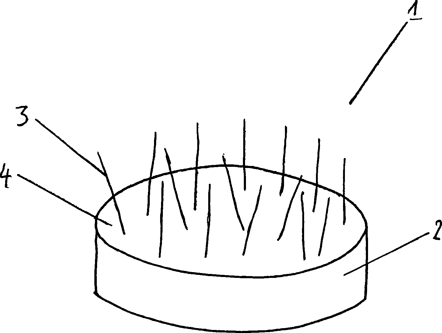
Optischer Sensor (1) mit einem optisch transparenten Trägerelement (2) und wenigstens einem daran angeordneten Nanodraht (3) aus einem dielektrischen Material, dadurch gekennzeichnet, dass der Nanodraht (3) in einem Spektralbereich ausgehend vom nahen UV- bis zum nahen IR-Bereich optisch transparent ist, so dass der gesamte Sensor (1) von Anregungslicht durchlaufbar ist.Optical sensor (1) having an optically transparent carrier element (2) and at least one nanowire (3) made of a dielectric material, characterized in that the nanowire (3) is in a spectral range starting from the near UV to the near IR region is optically transparent, so that the entire sensor (1) of excitation light is passable.
Description
Die vorliegende Erfindung betrifft einen optischen Sensor mit einem Trägerelement und wenigstens einem daran angeordneten Nanodraht sowie ein Verfahren zur Herstellung eines optischen Sensors, bei dem zunächst eine Schablone auf zumindest einen Teil der Trägerelementoberfläche und anschließend ein Halbleitermaterial auf die mit der Schablone versehenen Trägerelementoberfläche aufgebracht wird.The present invention relates to an optical sensor having a carrier element and at least one nanowire arranged thereon and to a method for producing an optical sensor, in which first a template is applied to at least a part of the carrier element surface and then a semiconductor material is applied to the carrier element surface provided with the template.
Gattungsgemäße optische Sensoren weisen zur Erhöhung der Empfindlichkeit eine vergrößerte sensorisch wirksame Oberfläche auf, welche mit einem zu untersuchenden Analyten in Form einer Flüssigkeit oder eines Gases wechselwirkt, wodurch eine Änderung des optischen Signals solcher Sensoren erzeugt wird, welches Rückschlüsse auf die Eigenschaften des Analyten erlaubt. Die Erhöhung der Empfindlichkeit eines solchen Sensors wird durch eine Funktionalisierung/Sensibilisierung der Sensoroberfläche durch das Aufbringen einer funktionalisierenden chemischen oder biologischen Substanz in Form von Einzelmolekülen oder Molekülschichten, beispielsweise eines Indikatorfarbstoffes, eines DNA-Oligonukleotids, eines Proteins, eines Liganden oder eines Enzyms auf die Sensoroberfläche erzeugt, wobei sich die Empfindlichkeit des Sensors mit der Menge der an der Sensoroberfläche angeordneten funktionalisierenden Substanz erhöht. Duch eine Vergrößerung der sensorisch wirksamen Sensoroberfläche kann mehr funktionalisierende Substanz an dem Sensor angeordnet werden, wodurch folglich ein Sensor mit hoher Empfindlichkeit bereitgestellt werden kann.Generic optical sensors have an increased sensory surface to increase the sensitivity, which interacts with an analyte to be examined in the form of a liquid or gas, whereby a change in the optical signal of such sensors is generated, which allows conclusions about the properties of the analyte. The increase in sensitivity of such a sensor is achieved by functionalizing / sensitizing the sensor surface by applying a functionalizing chemical or biological substance in the form of single molecules or molecular layers, for example an indicator dye, a DNA oligonucleotide, a protein, a ligand or an enzyme Sensor surface generated, wherein the sensitivity of the sensor increases with the amount of arranged on the sensor surface functionalizing substance. By increasing the sensory sensor surface, more functionalizing substance can be placed on the sensor, thus providing a high sensitivity sensor.
Zur Vergrößerung der sensorisch wirksamen Sensoroberfläche ist es beispielsweise bekannt, einen Sensor aus porösem Material zu verwenden oder die Sensoroberfläche mit einer porösen Substanz zu beschichten. Durch diese Porenstruktur weisen solche Sensoren eine für die Funktionalisierung vergrößerte sensorisch wirksame Oberfläche auf, an welcher eine funktionalisierende Substanz gebunden werden kann.To increase the sensory sensor surface, it is known, for example, to use a sensor made of porous material or to coat the sensor surface with a porous substance. As a result of this pore structure, such sensors have an organoleptic surface which is enlarged for functionalization and to which a functionalizing substance can be bound.
Bei optischen Sensoren, für die keine optische Transparenz der sensorisch wirksamen Oberfläche gefordert wird, können beispielsweise poröses Korund oder poröses Silizium in Form von bulk-Material oder als Schicht auf einer Sensoroberfläche für die Ankopplung der Indikatormoleküle verwendet werden. Nachteilig bei der Verwendung von porösen Schichten oder Materialien für Sensoren ist, dass die Porenstruktur der sensorisch wirksamen Sensoroberfläche eine schlechte Zugänglichkeit bezüglich der Funktionalisierung mit Indikatormolekülen aufweist, was sich zudem negativ auf die Wechselwirkung der Sensoroberfläche mit den Molekülen eines zu untersuchenden Analyten auswirkt.In optical sensors, for which no optical transparency of the sensory surface is required, for example, porous corundum or porous silicon in the form of bulk material or as a layer on a sensor surface can be used for the coupling of the indicator molecules. A disadvantage of the use of porous layers or materials for sensors is that the pore structure of the sensory sensor surface has poor accessibility with respect to the functionalization with indicator molecules, which also has a negative effect on the interaction of the sensor surface with the molecules of an analyte to be examined.
Wesentlich vorteilhafter ist die Verwendung einer offenen Oberflächenstruktur durch Anordnung von Nanodrähten auf der Sensoroberfläche. Das große Aspektverhältnis (Länge zu Durchmesser) von Nanodrähten, als optimale Voraussetzung für eine Funktionalisierung mit chemischen und biologischen Substanzen, wird im Schrifttum seit einigen Jahren beschrieben. Ihre Verwendung für Sensoren beschränkte sich aber bisher auf elektrisch basierte Prinzipien. Dabei wird wenigstens ein Nanodraht aus Halbleitermaterial, vorwiegend aber aus dotiertem Silizium, in einer Feld-Effekt-Transistor-(FET)-Anordnung verwendet, wobei die Eigenschaft ausgenutzt wird, dass sich Oberflächenladungen und damit die Leitfähigkeit der Nanodrähte unter dem Einfluss des Analyten ändern.Much more advantageous is the use of an open surface structure by arranging nanowires on the sensor surface. The large aspect ratio (length to diameter) of nanowires, as an optimal condition for functionalization with chemical and biological substances, has been described in the literature for several years. Their use for sensors has so far been limited to electrically based principles. In this case, at least one nanowire made of semiconductor material, but predominantly of doped silicon, used in a field effect transistor (FET) arrangement, wherein the property is exploited that change surface charges and thus the conductivity of the nanowires under the influence of the analyte ,
Eine weitere Anwendung der vorbeschriebenen offenen Oberflächenstrukturen unter Verwendung von an einer Sensoroberfläche angeordneten Nanodrähten ist der Einsatz in Analysesystemen, welche auf SERS (Surface-Enhanced Raman Scattering) basieren. Beispielsweise offenbart die US-Patentanmeldung 2006/0038990 A1 ein SERS-Analysesystem, welches einen SERS-Sensor verwendet, der auf einem optischen Substrat angeordnete, chemisch funktionalisierte Nanodrähte aufweist. Mittels dieses SERS-Sensors kann beispielsweise eine Anregung der Nanodrähte durch eine Anregungslichtquelle erfolgen, wobei das Licht durch das optische Substrat zu den Nanodrähten geleitet werden kann. Die dadurch angeregten Nanodrähte erzeugen eine Vibration der funktionalisierenden Moleküle, welche daraufhin eine versetzte Raman-Strahlung abgeben, welche zur weiteren Auswertung detektiert werden kann. Ein weiterer SERS-Sensor mit SERS-aktiver Oberflächenstruktur ist aus der US-Patentanmeldung 2006/0146323 A1 bekannt, bei der die Nanodrähte jeweils mit einem Ende auf einem Substrat befestigt sind und an dem jeweils anderen Ende ein SERS-aktives Material aufweisen, welches sich von dem Material der Nanodrähte unterscheidet. Die SERS-aktiven Enden der Nanodrähte können entsprechend funktionalisiert sein.Another application of the above-described open surface structures using nanowires arranged on a sensor surface is the use in analysis systems based on SERS (surface-enhanced Raman scattering). For example, US patent application 2006/0038990 A1 discloses a SERS analysis system using a SERS sensor having chemically functionalized nanowires arranged on an optical substrate. By means of this SERS sensor, for example, an excitation of the nanowires by an excitation light source, wherein the light can be passed through the optical substrate to the nanowires. The nanowires stimulated thereby generate a vibration of the functionalizing molecules, which then emit an offset Raman radiation, which can be detected for further evaluation. Another SERS sensor with SERS-active surface structure is known from the US patent application 2006/0146323 A1, in which the nanowires are each attached at one end to a substrate and at the other end of a SERS-active material having, which different from the material of the nanowires. The SERS-active ends of the nanowires may be functionalized accordingly.
Die Schrift von Xiaohong An, et. el.: SiO2 Nanowires Growing on Hexagonally Arranged Circular Patterns Surrounded by TiO2 Films. In: J. Phys. Chem. B 2006, 110, 222–226; 6. Dez. 2005 lehrt, dass für die Synthese von neuartigen Verbundarchitekturen ein effektiver Ansatz existiert, in dem SiO2-Nanodrähte auf sechseckig angeordneten Kreismustern wachsen, die von TiO2-Filmen auf Si-Substrat umgeben sind. Zuerst wird dazu eine Lösung-Tauch-Schablonenstrategie verwendet, um TiO2-Filme mit hexagonal angeordneten Poren auf einem Au-beschichteten Si-Substrat zu erzeugen, was zu sechseckig angeordneten kreisförmigen Mustern von Katalysatoren führt, die von TiO2-Filmen umgeben sind. Danach führen die gemusterten Katalysatoren zum Wachstum von SiO2-Nanodrähte mit den ursprünglichen TiO2-Filmen, die erhalten werden, wobei die Verbundstrukturen verwirklicht werden. Solche Verbundarchitekturen kombinieren die Photolumineszenz-Eigenschaften der beiden Komponenten und stellen auch eine günstigere photolumineszenz-Eigenschaft dar und legen eine Grundlage für zukünftige fortschrittliche nano-optoelektronische Bauelemente.The Scripture of Xiaohong An, et. el .: SiO 2 Nanowires Growing on Hexagonally Arranged Circular Patterns Surrounded by TiO 2 Films. In: J. Phys. Chem. B 2006, 110, 222-226; Dec. 6, 2005 teaches that an effective approach exists for the synthesis of novel composite architectures in which SiO 2 nanowires grow on hexagonal circular patterns surrounded by TiO 2 films on Si substrate. First, a solution immersion template strategy is used to produce TiO 2 films with hexagonal pores on an Au-coated Si substrate, which leads to hexagonal circular patterns of catalysts surrounded by TiO 2 films. Thereafter, the patterned catalysts result in the growth of SiO 2 nanowires with the original TiO 2 films that are obtained, thereby realizing the composite structures. Such composite architectures combine the photoluminescent properties of the two components and also provide a more favorable photoluminescent property and lay a foundation for future advanced nano-optoelectronic devices.
Die Publikation von Ki-Hong Lee, et. al.: Direct growth of amorphous silica nanowires by solid state tranformation of SiO2 films. In: Chemical Physics Letters 383 (2004) 380–384, 5. Dez. 2003 lehrt amorphe Siliciumdioxid-Nanodrähte, welche durch direkte Festkörpertransformation aus Siliciumdioxidfilmen hergestellt werden. Dabei wachsen Kieselsäure-Nanodrähte bei einer Temperatur von 1050°C auf TiN/Ni/SiO2/Si-Substraten während des Glühens in H2 oder einer H2:CH4-Mischung auf. Dabei wird Titannitrid-Folien verwendet, um eine Festkörperreaktion mit Siliciumdioxid-Filmen auf Silicium-Wafern zu induzieren, um Siliciumatome wachsen zu lassen. Die Titannitrid-Schichten induzieren hierbei die Diffusion von Silizium und Sauerstoff zu der Oberfläche durch einen in den Filmen eingebauten Spannungsgradienten.The publication by Ki-Hong Lee, et. al .: Direct growth of amorphous silica nanowires by solid state transformation of SiO 2 films. In: Chemical Physics Letters 383 (2004) 380-384, 5 Dec. 2003 teaches amorphous silica nanowires, which are prepared by direct solid-state transformation of silicon dioxide films. Silica nanowires grow at a temperature of 1050 ° C on TiN / Ni / SiO 2 / Si substrates during annealing in H 2 or a H 2 : CH 4 mixture. Titanium nitride films are used to induce a solid state reaction with silicon dioxide films on silicon wafers to grow silicon atoms. The titanium nitride layers induce the diffusion of silicon and oxygen to the surface through a voltage gradient built into the films.
Die Schrift von Praveen Kumar Sekhar, et al.: Slective growth of silica nanowires in silicon catalysed by Pt thin film. In: Nanotechnology 17 (2006) 4606–4613; 29. Aug. 2006 lehrt das selektive Wachstum von amorphen Siliciumdioxid-Nanodrähten auf einem mit Pt-Dünnfilm welches auf einem Siliciumwafer abgeschieden wird. Die Nanodrähte wachsen dabei mit einem Durchmesser von 50 bis 500 nm. Diese nach oben gewachsenen Nanodrähte zeigen unter Anregung eine Photolumineszenz mit einer stabilen Emission von blauem Licht bei 430 nm. Die Veränderung der Saatschichtdicke der Pt-Folie von 2 bis 100 nm führt dabei dazu, dass eine über 10 nm dicke kontinuierliche Schicht aus Pt2Si auf der Oberfläche entsteht, was das Wachstum von Nanodrähten hemmt. Die Selektivität zur Pt-Dicke wird ausgenutzt, um Bereiche von Nanodrähten zu erzeugen, die gleichzeitig mit Silizid (Pt2Si) in einer einzigen Ofenbehandlung verbunden werden. Dieser neuartige Ansatz hat die Gateways für die Realisierung von Hybrid-Verbindungen in Silizium für verschiedene nano-optische Anwendungen, wie bspw. die Herstellung niederdimensionaler Wellenleiter für die funktionelle Mikrophotonik, Scan-Nahfeldmikroskopie und Nano-Antennen geöffnet.The paper by Praveen Kumar Sekhar, et al .: Slective growth of silica nanowires in silicon catalysed by Pt thin film. In: Nanotechnology 17 (2006) 4606-4613; Aug. 29, 2006 teaches the selective growth of amorphous silica nanowires on a Pt thin film deposited on a silicon wafer. The nanowires grow with a diameter of 50 to 500 nm. These upwardly grown nanowires exhibit under excitation a photoluminescence with a stable emission of blue light at 430 nm. The change in the seed layer thickness of the Pt film from 2 to 100 nm leads to this in that an over 10 nm thick continuous layer of Pt 2 Si is formed on the surface, which inhibits the growth of nanowires. The selectivity to Pt thickness is exploited to create regions of nanowires that are simultaneously bonded to silicide (Pt 2 Si) in a single furnace treatment. This novel approach has opened the gateways for the realization of hybrid silicon interconnects for various nano-optical applications, such as the fabrication of low dimensional waveguides for functional microphotonics, near-field scanning microscopy, and nano-antennas.
Ki-Hong Lee, et. al.: Amorphous silica nanowires grown by the vaporsolid mechanism, In: Chemical Physics Letters 376 (2003) 498–503, 9. July 2003 offenbart Siliciumdioxid-Nanodrähte, welche unter Verwendung von Siliciumdioxid-Nanopartikeln als Wachstumskatalysator bei 1050°C unter dem Einfluss eines Gemisches aus CH4 und H2 synthetisiert wurden. Die Siliciumdioxid-Nanopartikel liefern dabei Silizium- und Sauerstoff-Atome für die Bildung der Nanodrähte und dienen gleichzeitig als Wachstumsort.Ki-Hong Lee, et. al.: Amorphous silica nanowires grown by the vaporsolide mechanism, In: Chemical Physics Letters 376 (2003) 498-503, 9th July 2003 discloses silica nanowires using silica nanoparticles as a growth catalyst at 1050 ° C under the influence a mixture of CH 4 and H 2 were synthesized. The silica nanoparticles provide silicon and oxygen atoms for the formation of the nanowires and also serve as a growth site.
Somit offenbaren die zuvor stehenden vier Schriften u. a. Vorrichtungen mit einem optisch transparenten Trägerelement und wenigstens einem daran angeordneten Nanodraht aus einem dielektrischen Material.Thus, the above four fonts u. a. Devices with an optically transparent support member and at least one arranged thereon nanowire of a dielectric material.
Der Nachteil dieser technischen Lösungen und der Nachteil der darauf basierenden Sensoren liegt darin, dass die Nanodrähte, welche aus einem dielektrischen Material bestehen, optisch nicht transparent sind, was dazu führt, dass sie (und damit der gesamte Sensor) nicht in einem Spektralbereich vom nahen UV- bis zum nahen IR-Bereich von Anregungslicht durchlaufen werden können. Damit sind diese technischen Lösungen für die Schaffung optischer Sensoren für optische Untersuchungen von Analyten ungeeignet.The disadvantage of these technical solutions and the disadvantage of the sensors based thereon is that the nanowires, which consist of a dielectric material, are optically not transparent, which means that they (and thus the entire sensor) are not in a spectral range from the near UV can be traversed to the near IR range of excitation light. Thus, these technical solutions for the creation of optical sensors for optical analysis of analytes are unsuitable.
Die Aufgabe der vorliegenden Erfindung besteht somit darin, einen optischen Sensor anzugeben, der für optische Untersuchungen von Analyten einsetzbar ist.The object of the present invention is thus to provide an optical sensor which can be used for optical investigations of analytes.
Diese Aufgabe wird durch einen optischen Sensor gemäß Anspruch 1 gelöst. Vorteilhafte Ausgestaltungen werden in den nachgeordneten Ansprüchen angegeben.This object is achieved by an optical sensor according to
Erfindungsgemäß besteht der wenigstens eine Nanodraht aus einem dielektrischen Material. Hierdurch wird gewährleistet, dass der Nanodraht in einem Spektralbereich ausgehend vom NUV(nahen UV)- bis zum NIR(nahen IR)-Bereich optisch transparent ist. Wird zudem für das Trägerelement ein optisch transparentes Material, wie beispielsweise ein Glassubstrat, gewählt, so ist der gesamte Sensor optisch transparent und es kann beispielsweise eine Untersuchung eines Analyten erfolgen, bei der ein Anregungslicht auf einer Seite des Sensors in diesen eintritt, ihn durchläuft und auf der anderen Seite des Sensors detektiert wird, was bei Sensoren aus dem Stand der Technik unmöglich ist und daher eine sehr hohe Flexibilität bezüglich des Einsatzes eines erfindungsgemäßen Sensors in der Praxis bedeutet.According to the invention, the at least one nanowire is made of a dielectric material. This ensures that the nanowire is optically transparent in a spectral range starting from the NUV (near UV) to the NIR (near IR) region. If, in addition, an optically transparent material, such as a glass substrate, is selected for the carrier element, then the entire sensor is optically transparent and, for example, an analysis of an analyte can take place in which an excitation light enters, passes through, and on one side of the sensor is detected on the other side of the sensor, which is impossible in sensors of the prior art and therefore means a very high flexibility with respect to the use of a sensor according to the invention in practice.
Im Rahmen der Erfindung können ebenso mehrere Nanodrähte an dem Trägerelement angeordnet sein, wobei sich die Anzahl der Nanodrähte an dem jeweiligen Einsatzzweck des entsprechenden Sensors orientieren kann. Vorzugsweise handelt es sich bei dem Nanodraht/den Nanodrähten um gewachsene Festkörperstrukturen mit Durchmessern von etwa 10 nm bis einigen 100 nm und mit Längen von etwa 1 μm bis zu einigen Mikrometern. Sie werden bevorzugt aus einkristallinem Silizium gebildet, und nachträglich durch thermische Oxidation zu amorphem Siliziumoxid, insbesondere Siliziumdioxid, umgewandelt, um im NUV- bis NIR-Spektralbereich transparente Nanodrähte zu erzeugen. Der Nanodraht/die Nanodrähte besitzt/besitzen zwei Enden, von denen ein Ende entsprechend eines Wachstumsprozesses auf der Oberfläche des Trägerelementes mit diesem verbunden ist. Mehrere Nanodrähte sind beispielsweise in Abständen untereinander von einigen 10 nm bis zu wenigen Mikrometern auf der Trägerelementoberfläche angeordnet. Der Abstand der Nanodrähte untereinander kann definiert (periodische Anordnung) oder auch völlig willkürlich (zufällig) sein. Die Form des Nanodrahtes/der Nanodrähte kann beispielsweise gerade, gebogen, verkrümmt oder verwunden sein. Die Ausrichtung des Nanodrahtes/der Nanodrähte in Bezug zur Trägerelementoberfläche kann senkrecht, unter definiertem Winkel oder zufällig ausgebildet sein. Voraussetzung für die Ausrichtung unter einem bestimmten einheitlichen Winkel zur Trägerelementoberfläche ist, dass die für das Wachstum maßgebliche Oberfläche (Wachstumsunterlage) eine einheitliche Kristallorientierung (Einkristallinität) besitzt und die Gitterkonstante dieser Kristallstruktur die Voraussetzung für ein epitaktischen Wachstumsprozess einkristalliner Nanodrähte bietet. Eine solche Ausführungsform ist beispielsweise dadurch erreichbar, dass mittels des VLS(vapor liquid solid)-Verfahrens Silizium-Nanodrähte auf einer einkristallinen Siliziumoberfläche wachsen. Für ein einheitliches Wachstum von Silizium-Nanodrähten in die der Kristallorientierung entsprechenden Raumrichtungen ist eine weitere Voraussetzung, dass sich auf der Siliziumoberfläche kein natives Oxid befindet.In the context of the invention, a plurality of nanowires may also be arranged on the carrier element, it being possible for the number of nanowires to be oriented to the respective intended use of the corresponding sensor. Preferably, the nanowire / nanowires are Grown solid structures with diameters of about 10 nm to several 100 nm and with lengths of about 1 micron to a few microns. They are preferably formed of monocrystalline silicon, and subsequently converted by thermal oxidation to amorphous silicon oxide, in particular silicon dioxide, in order to produce transparent nanowires in the NUV to NIR spectral range. The nanowire / nanowires have two ends, one end of which is connected to it in accordance with a growth process on the surface of the support member. Several nanowires are arranged, for example, at intervals of a few 10 nm to a few micrometers on the carrier element surface. The distance between the nanowires can be defined (periodic arrangement) or completely arbitrary (random). The shape of the nanowire / nanowires may, for example, be straight, curved, curved or twisted. The orientation of the nanowire / nanowires with respect to the support surface may be perpendicular, at a defined angle, or random. The prerequisite for alignment at a certain uniform angle to the support element surface is that the growth-relevant surface (growth support) has a uniform crystal orientation (single crystallinity) and the lattice constant of this crystal structure provides the precondition for an epitaxial growth process of single-crystalline nanowires. Such an embodiment can be achieved, for example, by growing silicon nanowires on a monocrystalline silicon surface by means of the VLS (vapor liquid solid) method. For a uniform growth of silicon nanowires in the spatial directions corresponding to the crystal orientation, another prerequisite is that there is no native oxide on the silicon surface.
Eine Ausführungsform von senkrecht zu der Trägerelementoberfläche angeordneten Silizium-Nanodrähten kann erreicht werden, indem mittels des Molekularstrahl-Epitaxie-Verfahrens (MBE, molecular beam epitaxy) auf einer (111)-Silizium-Oberfläche Silizium-Nanodrähte in [111]-Richtung wachsen. Hierbei wird die Tatsache ausgenutzt, dass das Wachstum in <111>-Richtung, gegenüber den <100>- und <110>-Richtungen, energetisch begünstigt ist. Zwar wachsen auch Nanodrähte in die Richtungen [-111], [1-11] und [-1-11], diese sind aber infolge ihres flachen Wachstumswinkels zur Oberfläche sowie der Ausbildung einer 2D-Siliziumschicht auf der Trägerelementoberfläche nicht sichtbar, da sie in die 2D-Schicht eingebettet sind.An embodiment of silicon nanowires arranged perpendicular to the support element surface can be achieved by growing [111] silicon nanowires by means of the molecular beam epitaxy (MBE) method on a (111) silicon surface. This exploits the fact that the growth in the <111> direction, compared to the <100> and <110> directions, is energetically favored. Although nanowires also grow in the directions [-111], [1-11], and [-1-11], these are not visible on the surface of the substrate due to their shallow growth angle to the surface and the formation of a 2D silicon layer the 2D layer are embedded.
Da ein Trägerelement aus einkristallinem Silizium, beispielsweise in Form eines Siliziumwafers, der Forderung nach Transparenz im NUV- bis NIR-Spektralbereich nicht genügt und auch eine thermische Oxidation des Siliziums bereits im Dickenbereich von einigen Mikrometern beträchtlichen technologischen und zeitlichen Aufwand erfordert, kann beispielsweise eine geeignet dünne einkristalline oder auch polykristalline Siliziumschicht, welche nach Abschluß des Nanodraht-Wachstumsprozesses thermisch oxidiert werden kann, auf einem die geforderte Transparenz bietenden Trägerelement angeordnet werden. Eine weitere Möglichkeit eines epitaktischen Wachstums von einkristallinen Si-Nanoschichten auf einem im NUV-NIR-Spektralbereich transparenten Trägersubstrat zu erreichen, wird durch eine transparente einkristalline Cer(IV)-oxid-Schicht (CeO2) auf einem Saphir-Substrat (Al2O3, R-Schnitt) erreicht.Since a carrier element made of monocrystalline silicon, for example in the form of a silicon wafer, does not meet the requirement for transparency in the NUV to NIR spectral range and also requires thermal oxidation of the silicon in the thickness range of a few micrometers considerable technological and time expenditure, for example, a suitable Thin single-crystalline or polycrystalline silicon layer, which can be thermally oxidized after completion of the nanowire growth process, are arranged on a carrier element providing the required transparency. A further possibility of achieving epitaxial growth of monocrystalline Si nanosheets on a carrier substrate which is transparent in the NUV-NIR spectral range is achieved by a transparent monocrystalline cerium (IV) oxide layer (CeO 2 ) on a sapphire substrate (Al 2 O 3 , R-section).
Unter Verwendung des VLS-Verfahrens zur Herstellung der Nanodrähte kann mittels geeigneter Strukturierungstechniken (lithografische Verfahren) eine geordnete, periodische Anordnung der Nanodrähte auf der Trägerelementoberfläche realisiert werden.Using the VLS method for producing the nanowires, an ordered, periodic arrangement of the nanowires on the carrier element surface can be realized by means of suitable structuring techniques (lithographic methods).
Als optischer Sensor kann beispielsweise ein auch im NUV- bis NIR-Spektralbereich optisch transparentes, planares Trägerelement mit Nanodrähten, eine Lichtleitfaser mit auf der Faserstirnfläche der Lichtleitfaser angeordneten Nanodrähten, eine Lichtleitfaser mit auf ihrer zylindrischen Oberfläche angeordneten Nanoschichten, eine zu einer Spitze verjüngt ausgebildete Lichtleitfaser mit auf der Mantelfläche im Bereich der Spitze angeordneten Nanodrähten oder ein planares Trägerelement mit optisch transparenter Schicht, an der die Nanodrähte angeordnet sind, verwendet werden.As an optical sensor, for example, also in the NUV to NIR spectral range optically transparent, planar support element with nanowires, an optical fiber with arranged on the fiber end face of the optical fiber nanowires, an optical fiber arranged on its cylindrical surface nanolayers, tapered to a tip formed optical fiber with arranged on the lateral surface in the region of the tip nanowires or a planar support element with an optically transparent layer, on which the nanowires are arranged, can be used.
Wird für das Trägerelement ein optisch transparentes Material gewählt, wobei die Nanodrähte im NUV- bis NIR-Spektralbereich optisch transparent sind, ist eine optische Abfrage der Wechselwirkung zwischen Analyt und funktionalisierten Nanodrähten von der Trägerelementseite des Sensors, sowohl für die optische Anregung, als auch die optische Detektion möglich, was für den Aufbau sehr kompakter Sensoren von großem Vorteil ist. Bei nicht optisch transparenten Trägerelementen ist die Anregung und Detektion nur über die Analytseite möglich, was nicht nur einen kompakten Sensoraufbau verhindert, sondern sich auch nachteilig bei trüben oder streuenden Analyten auswirkt. Der Einsatz transparenter Trägerelemente gewährleistet zudem das Aufbringen von Filterschichten auf einem Trägerelement, um zum Beispiel das Anregungslicht bei der Detektion eines Fluoreszenzlichtes zu unterdrücken.If an optically transparent material is selected for the carrier element, wherein the nanowires in the NUV to NIR spectral range are optically transparent, an optical interrogation of the interaction between analyte and functionalized nanowires from the carrier element side of the sensor, both for the optical excitation, and the optical detection possible, which is for the construction of very compact sensors of great advantage. In the case of non-optically transparent carrier elements, the excitation and detection is possible only via the analyte side, which not only prevents a compact sensor structure, but also adversely affects turbid or scattering analytes. The use of transparent carrier elements also ensures the application of filter layers on a carrier element in order to suppress, for example, the excitation light in the detection of a fluorescent light.
Zur Untersuchung eines bestimmten Analyten, wird die durch die Oberfläche der Nanodrähte und die zwischen den Nanodrähten befindlichen Bereiche der Trägerelementoberfläche gebildete sensorisch wirksame Oberfläche mit chemischen oder biologischen Substanzen funktionalisiert, wobei die Art der funktionalisierenden Substanz an den jeweiligen Anwendungszweck des Sensors angepasst werden und die Funktionalisierung der Trägerelementoberfläche beispielsweise bereichsweise mit verschiedenen Substanzen erfolgen kann, um auch einen Analyten mit mehreren verschiedenen Komponenten mit einem einzigen Sensor untersuchen zu können.To examine a particular analyte, the sensory surface formed by the surface of the nanowires and the areas of the support element surface located between the nanowires is chemically or chemically sensitized functionalized biological substances, wherein the type of functionalizing substance are adapted to the particular application of the sensor and the functionalization of the carrier element surface, for example, can be carried out with different substances in areas to investigate an analyte with several different components with a single sensor can.
Folgende beispielhafte Funktionalisierungen/Sensibilisierungen der sensorisch wirksamen Oberfläche und sich daraus ergebende Wechselwirkungen sind möglich:
- • Sensibilisierung mit Fluoreszenz-Farbstoff-Molekülen, beispielsweise zur Messung des pH-Wertes eines Analyten
- • Sensibilisierung mit Fluoreszenz-Farbstoff zum Nachweis von Gasen und Dämpfen (bspw. O2, CO2, NH3)
- • Sensibilisierung mit mit Fluoreszenz-Farbstoff zum Analyt-Nachweis in Flüssigkeiten (bspw. SO3 über Fluoreszenzlöschung)
- • Sensibilisierung mit DNA-Fängermolekülen zur Detektion von Analyt-DNA über fluoreszenzmarkierte Analyt-DNA-Bindungsreaktionen
- • Sensibilisierung mit Proteinen zum Nachweis von Antikörper(Immungluboline)/Antigen(Immunogen)-Reaktionen
- • Sensibilisierung mit Liganden zum Nachweis fluoreszenzmarkierter Analyten
- • Sensitization with fluorescent dye molecules, for example, to measure the pH of an analyte
- • sensitization with fluorescent dye for the detection of gases and vapors (eg O 2 , CO 2 , NH 3 )
- Sensitization with fluorescence dye for analyte detection in liquids (eg SO 3 via fluorescence quenching)
- Sensitization with DNA capture molecules to detect analyte DNA via fluorescently labeled analyte-DNA binding reactions
- • Sensitization with proteins to detect antibody (immunoluboline) / antigen (immunogen) reactions
- • Sensitization with ligands to detect fluorescently labeled analytes
Zweckmäßigerweise sind die funktionalisierenden Moleküle kovalent an die sensorisch wirksame Oberfläche gebunden.Conveniently, the functionalizing molecules are covalently bound to the sensory surface.
Für die oben genannten Wechselwirkungsmechanismen kommen beispielsweise folgende Messmethoden in Frage:
- – Absorption, Transmission, Streuung, Reflexion/Remission
- – Fluoreszenzanregung und Quantifizierung des Fluoreszenzsignals
- – spektrale Auswertung oder Intensitätsauswertung
- – Evaneszenz-Feld-Wechselwirkung
- – Optisch plasmonische Wechselwirkungen
- - absorption, transmission, scattering, reflection / remission
- - Fluorescence excitation and quantification of the fluorescence signal
- - Spectral evaluation or intensity evaluation
- - Evanescent field interaction
- - Optically plasmonic interactions
Eine vorteilhafte Ausgestaltung der Erfindung sieht vor, dass das dielektrische Material ein Siliziumoxid, vorzugsweise Siliziumdioxid, ist. Insbesondere die Verwendung von Siliziumdioxid für die Nanodrähte bringt die gewünschte Transparenz der Nanodrähte in dem NUV- bis NIR-Spektralbereich.An advantageous embodiment of the invention provides that the dielectric material is a silicon oxide, preferably silicon dioxide. In particular, the use of silicon dioxide for the nanowires brings the desired transparency of the nanowires in the NUV to NIR spectral range.
Nach einer weiteren vorteilhaften Ausgestaltung der Erfindung besteht das Trägerelement aus Silizium (Si), Quarzglas (SiO2) oder Saphir (Al2O3, R-Schnitt). Welches dieser Materialien für das Trägerelement verwendet wird, hängt von der jeweiligen Ausgestaltung des Sensors ab. Ist beispielsweise neben der Transparanz der Nanodrähte in dem genannten Bereich auch die Transparenz des Trägerelementes gefordert, ist es vorteilhaft, für das Trägerelement statt Silizium Quarzglas oder andere hochtemperaturfeste Gläser oder Kristalle, wie beispielsweise Saphir, zu verwenden. Hochtemperaturfeste Materialien, wie etwa Quarzglas oder Saphir, sind zudem beständig gegenüber der Oxidationstemperatur von etwa 900°C bei der thermischen Oxidation der Nanodrähte. Besonders bevorzugt finden solche Materialien Anwendung, die sowohl die spektrale Transmission in dem genannten Spektralbereich, als auch eine für das epitaktische Wachstum günstige Kristallstruktur besitzen. Wie bereits zuvor stehend ausgeführt, bietet sich hierfür die Kombination einer dünnen (wenige 10 nm) und damit transparenten einkristallinen Cer(IV)-oxid-Schicht auf einem dünnen Saphir-Trägersubstrat (R-Schnitt) an. Die Cer(IV)-oxid-Schicht bietet mit ihrer kubischen Kristallstruktur die Voraussetzung für einen epitaktischen Wachstumsprozess der Si-Nanodrähte.According to a further advantageous embodiment of the invention, the carrier element consists of silicon (Si), quartz glass (SiO 2 ) or sapphire (Al 2 O 3 , R-section). Which of these materials is used for the support member depends on the particular configuration of the sensor. If, for example, in addition to the transparency of the nanowires in the named region, the transparency of the carrier element is required, it is advantageous to use quartz glass or other high-temperature-resistant glasses or crystals, such as sapphire, instead of silicon for the carrier element. High-temperature resistant materials such as quartz glass or sapphire are also resistant to the oxidation temperature of about 900 ° C in the thermal oxidation of the nanowires. Particular preference is given to materials which have both the spectral transmission in the abovementioned spectral range and a crystal structure favorable for epitaxial growth. As already stated above, the combination of a thin (a few 10 nm) and therefore transparent single-crystal cerium (IV) oxide layer on a thin sapphire carrier substrate (R-cut) is suitable for this purpose. The cerium (IV) oxide layer with its cubic crystal structure is the prerequisite for an epitaxial growth process of the Si nanowires.
Gemäß einer weiteren vorteilhaften Ausgestaltung der Erfindung ist zwischen dem Trägerelement und dem wenigstens einen Nanodraht eine optisch transparente Schicht angeordnet. Diese Ausgestaltung ist insbesondere dann von Vorteil, wenn das Trägerelement aus Silizium besteht und somit nicht optisch transparent ist. In diesem Fall wird mittels der transparenten Schicht eine Schicht-Wellenleiteranordnung geschaffen, bei welcher das evanescente Feld des in der Wellenleiterschicht geführten Lichtes für die sensorische Wechselwirkung mit dem Analyten genutzt wird.According to a further advantageous embodiment of the invention, an optically transparent layer is arranged between the carrier element and the at least one nanowire. This embodiment is particularly advantageous if the carrier element consists of silicon and thus is not optically transparent. In this case, a layer waveguide arrangement is created by means of the transparent layer, in which the evanescent field of the light guided in the waveguide layer is used for the sensory interaction with the analyte.
Ferner besteht die optisch transparente Schicht in vorteilhafter Ausgestaltung der Erfindung aus Siliziumdioxid, um die gewünschte optische Transparenz aufzuweisen. Denkbar sind aber auch andere Materialien für die optisch transparente Schicht, welche den jeweiligen Anforderungen an den Sensor gewachsen sind.Furthermore, in an advantageous embodiment of the invention, the optically transparent layer consists of silicon dioxide in order to have the desired optical transparency. Also conceivable are other materials for the optically transparent layer, which have grown to the respective requirements of the sensor.
Des Weiteren wird mit der vorliegenden Erfindung ein Verfahren zur Herstellung eines optischen Sensors vorgeschlagen, welcher über einen großen Spektralbereich optisch transparent und somit für optische Untersuchungen von Analyten geeignet ist.Furthermore, the present invention proposes a method for producing an optical sensor which is optically transparent over a large spectral range and thus suitable for optical investigations of analytes.
Das erfindungsgemäße Verfahren zur Herstellung eines optischen Sensors, bei dem zunächst ein Bereitstellen eines Trägerelementes, ein Aufbringen einer Schablone aus geeignetem Schablonenmaterial auf zumindest einen Teil der Trägerelementoberfläche und ein Aufbringen von Halbleitermaterial auf die mit der Schablone versehene Trägerelementoberfläche erfolgen, ist erfindungsgemäß dadurch gekennzeichnet, dass das Schablonenmaterial nach dem Aufbringen des Halbleitermaterials entfernt und anschließend das Halbleitermaterial oxidiert wird. Durch die Oxidation des Halbleitermaterials wird erreicht, dass dieses in dem NUV- bis NIR-Spektralbereich transparent wird, was sich positiv auf die Anwendungsflexibilität eines entsprechenden Sensors auswirkt.The inventive method for producing an optical sensor, in which initially providing a carrier element, applying a template made of suitable stencil material on at least a part of the carrier element surface and applying a semiconductor material to the provided with the template carrier element surface, according to the invention is characterized in that removes the stencil material after applying the semiconductor material and then oxidizes the semiconductor material becomes. The oxidation of the semiconductor material ensures that it becomes transparent in the NUV to NIR spectral range, which has a positive effect on the application flexibility of a corresponding sensor.
Die Herstellung von beispielsweise Siliziumdioxid-Nanodrähten basiert zum Beispiel auf der Herstellung von Silizium-Nanodrähten auf einer Trägerelementoberfläche. Für die Erzeugung von Silizium-Nanodrähten bedient man sich zum Beispiel des VLS-Verfahrens. Dazu wird bei hohen Temperaturen ein Gas, welches das Nanodraht-Material (hier Silizium) in atomarer Form, wie etwa Silizium, oder als Bestandteil eines Moleküls (wie z. B. des Silans (SiH4)) enthält, über eine beispielsweise mit Goldteilchen versehene Trägerelementoberfläche geleitet. Die Goldteilchen bilden eine Schablone mit flachen Inseln, Kügelchen oder kugelähnlichen Ausgestaltungen, welche in zufälliger oder geordneter Verteilung auf der Trägerelementoberfläche angeordnet sein können, was auch als Goldschablone (engl. Goldtamplate) bezeichnet wird. Ihre Abmessungen liegen in der Größenordnung weniger Nanometer bis einige 100 Nanometer. Wird Silizium als Trägerelement verwendet, bilden sich bei Temperaturen oberhalb 370°C (Au/Si-Eutektikum) Legierungs-Schmelztropfen auf der Trägerelementoberfläche, deren flüssige Oberfläche, zum Beispiel bei Verwendung von Silan, als Katalysator zum Aufbrechen des Moleküls dient. Das Ziel ist der Einbau von Siliziumatomen in den Legierungsschmelztropfen. Im weiteren Verlauf werden die Siliziumatome in dem flüssigen Legierungstropfen gelöst, bis es bei Übersättigung zur Keimbildung und letztendlich zur Kristallisation der Siliziumatome kommt. Diese findet bevorzugt an der Grenzfläche flüssig/fest mit dem Ergebnis des Wachstums von Silizium-Nanodrähten statt. Die kristallographische Orientierung der Nanodrähte stimmt hierbei mit der Orientierung der Unterlage überein. Aus jedem Legierungs-Schmelztropfen wachst in der Regel ein Silizium-Nanodraht mit einem Durchmesser ähnlich dem des Legierungs-Schmelztropfendurchmessers.For example, the fabrication of silicon dioxide nanowires is based on the production of silicon nanowires on a support surface. For the production of silicon nanowires one uses, for example, the VLS method. For this, at high temperatures, a gas containing the nanowire material (here, silicon) in atomic form, such as silicon, or as part of a molecule (such as the silane (SiH 4 )) via, for example, gold particles directed carrier element surface passed. The gold particles form a template with shallow islands, globules, or sphere-like configurations, which may be arranged in random or ordered distribution on the support element surface, which is also referred to as gold templates. Their dimensions are on the order of a few nanometers to a few 100 nanometers. When silicon is used as the carrier element, alloy melting drops form on the carrier element surface at temperatures above 370 ° C. (Au / Si eutectic), whose liquid surface, for example when using silane, serves as a catalyst for breaking up the molecule. The goal is the incorporation of silicon atoms in the alloy melt droplets. In the further course of the silicon atoms are dissolved in the liquid alloy drop until it comes to supersaturation nucleation and ultimately to the crystallization of the silicon atoms. This preferably takes place at the interface liquid / solid with the result of the growth of silicon nanowires. The crystallographic orientation of the nanowires coincides with the orientation of the substrate. From each alloy melt drop, a silicon nanowire having a diameter similar to that of the alloy melt drop diameter typically grows.
Um der Forderung nach optischer Tranzparenz der angeordneten Nanodrähte zu genügen, wird mittels thermischer Oxidation eine Strukturumwandlung der zuvor nach dem VLS-Verfahren hergestellten Silizium-Nanodrähte zu Siliziumdioxid-Nanodrähten durchgeführt. Eine derartige Umwandlung der Silizium- in eine Siliziumdioxid-Struktur ist mittels einer Trockenoxidation unter reiner Sauerstoffatmosphäre oder Feuchtoxidation in Gegenwart von Wasserdampf möglich. Durch die Trockenoxidation lassen sich jedoch dichtere und homogenere Oxide als bei der Feuchtoxidation realisieren. Je nach Durchmesser der Silizium-Nanodrähte beläuft sich die Oxidationszeit auf 6 bis 9 Stunden bei einer Prozesstemperatur von 900°C in trockenem Sauerstoff. Ziel ist das Erreichen einer vollständigen Oxidation, ohne Verbleib eines Siliziumrestkerns in einem Nanodraht.In order to meet the requirement for optical transparency of the arranged nanowires, structural conversion of the silicon nanowires previously produced by the VLS method to silicon dioxide nanowires is carried out by means of thermal oxidation. Such a conversion of the silicon into a silicon dioxide structure is possible by means of a dry oxidation under pure oxygen atmosphere or moist oxidation in the presence of water vapor. By dry oxidation, however, denser and more homogeneous oxides than in the wet oxidation can be realized. Depending on the diameter of the silicon nanowires, the oxidation time amounts to 6 to 9 hours at a process temperature of 900 ° C in dry oxygen. The goal is to achieve complete oxidation without leaving a residual silicon core in a nanowire.
Da jene nach dem VLS-Verfahren hergestellten Silizium-Nanodrähte verfahrensbedingt am trägerelementfernen Ende einen Goldtropfen aufweisen, ist es notwendig, diesen vor der Oxidation zu entfernen. Hierzu wird zunächst die native Oxidhaut auf dem Gold und dem Silizium entfernt, indem das Trägerelement mit den daran angeordneten Silizium-Nanodrähten beispielsweise in 2%-iger Flusssäure für ca. 30 s geätzt wird. Unmittelbar danach kann das Gold mit einer Mischung aus konzentrierter Salpetersäure und konzentrierter Salzsäure (Mischungsverhältnis 1:3) bei Raumtemperatur vollständig entfernt werden, wobei die Ätzzeit ca. 30 s bis 60 s betragen kann.Since those silicon nanowires produced by the VLS process have a gold drop at the end remote from the carrier because of the process, it is necessary to remove them before the oxidation. For this purpose, the native oxide skin on the gold and the silicon is first removed by etching the carrier element with the silicon nanowires arranged thereon, for example in 2% hydrofluoric acid, for about 30 seconds. Immediately thereafter, the gold can be completely removed with a mixture of concentrated nitric acid and concentrated hydrochloric acid (mixing ratio 1: 3) at room temperature, the etching time can be about 30 s to 60 s.
Zur Verbesserung des epitaktischen Anwachsens der Silizium-Nanodrähte auf Quarzglasträgerelementoberflächen kann die Trägerelementoberfläche, welche für das Wachstum der Nanodrähte dienen soll, mit einer ca. 400 nm bis 600 nm dicken polykristallinen Siliziumschicht versehen werden. Realisiert werden kann dies durch Laserkristallisation einer auf der Trägerelementoberfläche abgeschiedenen amorphen Siliziumschicht. Diese polykristalline Siliziumoberfläche dient als Unterlage für die Herstellung der Goldschablone. Für die Goldschablonenherstellung auf der polykristallinen Siliziumoberfläche ist es günstig, dass das durch die Laserkristallisation entstandene Siliziumdioxid vor dem Aufbringen der Schablone zu entfernen, was sich vorteilhaft auf das epitaktische Wachstum auswirkt. Nach erfolgtem Wachstum der Nanodrähte kann die polykristalline Siliziumschicht gemeinsam mit den Nanodrähten mittels thermischer Oxidation in Siliziumdioxid umgewandelt werden.To improve the epitaxial growth of the silicon nanowires on quartz glass carrier element surfaces, the carrier element surface, which is to serve for the growth of the nanowires, be provided with an about 400 nm to 600 nm thick polycrystalline silicon layer. This can be realized by laser crystallization of an amorphous silicon layer deposited on the carrier element surface. This polycrystalline silicon surface serves as a base for the production of the gold template. For the production of gold stencils on the polycrystalline silicon surface, it is favorable to remove the silicon dioxide resulting from the laser crystallization before applying the stencil, which has an advantageous effect on the epitaxial growth. After growth of the nanowires, the polycrystalline silicon layer can be converted together with the nanowires by means of thermal oxidation in silicon dioxide.
Die Herstellung einer Goldschablone kann nach einer der folgenden Methoden erfolgen:
- a) Durch Tempern eines wenige Nanometer (1,5
nm bis - b) Abscheiden von Goldnanopartikeln mit definiertem einheitlichem Durchmesser etwa
im Bereich von 10 nm bis 100 nm aus einer Goldkolloidlösung, auf die Oberfläche eines Quarzglasträgerelementes mit oder ohne polykristalline Siliziumschicht. Dadurch entsteht eine willkürlich (statistisch) ausgebildete Goldschablone. Um die Kopplung der Goldnanopartikel zur Trägerelementoberfläche zu verbessern, kann die Trägerelementoberfläche zuvor mit speziellen cross-linker-Molekülen (z. B. 3-Aminopropyltriethoxysilan oder mit Poly-L-Lysin) aktiviert werden, an welchen die Goldnanopartikel chemisch oder elektrostatischankoppeln. Die Belegungsdichte kann durch die Konzentration der verwendeten Kolloidlösung beeinflusst werden. Die Durchmesserverteilung der Nanodrähte ist enger im Vergleich zu den Nanodrähten erzeugt durch getemperte Goldfilme. - c) Herstellung von in ihrer Gestalt regelmäßig, als auch periodisch geordneten Goldstrukturen mittels Strukturierung (Elektronenstrahllithographie) einer auf einer Trägerelementoberfläche zuvor nach den in a) benannten Verfahren abgeschiedenen Goldschicht. Die Größe der Goldstrukturen, als auch die Strukturperiode ist frei wählbar. Es kann hiermit ein sehr einheitlicher Durchmesser und Abstand der Nanodrähte erzeugt werden.
- d) Die Herstellung von Goldschichten mittels Molekularstrahl-Epitaxie (molecular beam epitaxy, MBE) besitzt gegenüber Sputtern, CVD oder galvanischer Abscheidung den entscheidenden Vorteil, dass das notwendige Entfernen von nativen Oxidschichten (z. B. durch einen Trocken-Ätzprozess) und die Abscheidung einer dünnen Goldschicht in-situ im UHV (10–10 mbar) erfolgen kann. Dadurch wird vermieden, dass sich vor dem Auftragen der Goldschicht wieder eine Oxidschicht bildet, wie es zum Beispiel bei den anderen genannten Methoden nicht ausgeschlossen werden kann. Anschließend erfolgt in derselben Anlage die Temperung der Goldschichten, um die Goldschablonen zu erzeugen.
- a) By annealing a few nanometers (1.5 nm to 3.5 nm) thick gold film on a carrier element surface at about 550 ° C. As a suitable method for producing defined thin gold layers are, for example, the sputtering process and the molecular beam epitaxy process to call. In the case of arranging a polycrystalline silicon layer produced by laser crystallization on a quartz glass substrate as a carrier element, spherical gold structures are formed due to the formation of a eutectic Au / Si melt and under the action of surface energy forces (surface tension). The initially largely continuous gold layer decays, so to speak, into single drops. In contrast, only flat irregular gold island structures are formed on a pure quartz glass surface, since no alloy melt is formed here. In both cases arises an arbitrarily (statistically) distributed gold template. The size of the obtained gold template is influenced only to a very small extent by the initial gold layer thickness. Starting from these templates grow nanowires with a wide diameter distribution.
- b) depositing gold nanoparticles of defined uniform diameter in the range of 10 nm to 100 nm from a gold colloid solution onto the surface of a quartz glass carrier element with or without a polycrystalline silicon layer. This creates an arbitrary (statistically) trained gold template. To enhance the coupling of the gold nanoparticles to the support surface, the support surface may be previously activated with specific cross-linker molecules (eg, 3-aminopropyltriethoxysilane or with poly-L-lysine) to which the gold nanoparticles chemically or electrostatically couple. The occupation density can be influenced by the concentration of the colloid solution used. The diameter distribution of the nanowires is narrower compared to the nanowires produced by annealed gold films.
- c) Production of regular, as well as periodically arranged, gold structures by means of structuring (electron beam lithography) of a gold layer previously deposited on a carrier element surface according to the processes mentioned in a). The size of the gold structures, as well as the structure period is arbitrary. It can hereby be produced a very uniform diameter and spacing of the nanowires.
- d) The production of gold layers by means of molecular beam epitaxy (MBE) has the decisive advantage over sputtering, CVD or electrodeposition that the necessary removal of native oxide layers (eg by a dry etching process) and deposition a thin gold layer can be made in-situ in UHV (10 -10 mbar). This avoids that before the application of the gold layer again forms an oxide layer, as it can not be excluded, for example, in the other methods mentioned. Subsequently, in the same system, the annealing of the gold layers to produce the gold stencils.
Die folgenden beispielhaften Abscheideverfahren zur Herstellung von Silizium-Nanodrähten unter Verwendung von Goldschablonen auf polykristallinen Silizium- und Quarzglasoberflächen können angewandt werden:
Chemische Gasphasenabscheidung (chemical vapor deposition, CVD).The following exemplary deposition techniques for making silicon nanowires using gold patterns on polycrystalline silicon and quartz glass surfaces may be used:
Chemical vapor deposition (CVD).
Bei diesem Verfahren wird Silan (SiH4) bei ca. 500°C und einem Druck von 0,5 mbar bis 5 mbar über das Trägerelement mit einer auf dessen Oberfläche angeordneten Goldschablone geleitet, wo es sich im Fall einer Siliziumoberfläche katalytisch an den entstandenen Au/Si-Tröpfchen zersetzt. Im Fall der Verwendung einer Quarzglasoberfläche mit einer Goldschablone liefert erst die Zersetzung des Silans während des CVD-Prozesses das Silizium für das Eutektikum. Durch Übersättigung, Keimbildung und Kristallisation kommt es dann an der Grenzfläche flüssig/fest der Au/Si-Tröpfchen zum Wachsen einkristalliner Silizium-Nanodrähte.In this method, silane (SiH 4 ) at about 500 ° C and a pressure of 0.5 mbar to 5 mbar passed over the support member with a gold stencil arranged on the surface, where it catalytically in the case of a silicon surface of the resulting Au / Si droplets decomposed. In the case of using a quartz glass surface with a gold template, it is only the decomposition of the silane during the CVD process that provides the silicon for the eutectic. By supersaturation, nucleation and crystallization it then comes at the interface liquid / solid of the Au / Si droplets for growing monocrystalline silicon nanowires.
Herstellung von Silizium-Nanodrähten mittels Elektronenstrahlverdampfung (electron beam evaporation, EBE).Production of silicon nanowires by electron beam evaporation (EBE).
Bei diesem Verfahren wird bei einem Druck von 10–6 mbar bis 10–7 mbar und einer Temperatur von 475°C bis 550°C ein Silizium-Dampf über die Trägerelementoberfläche mit der darauf angeordneten Goldschablone geleitet. Das Wachstum der Nanodrähte ist äquivalent dem vorbeschriebenen Prozess, mit dem Unterschied, dass sich bei diesem Verfahren eine zusätzliche 2D-Siliziumschicht auf der Substratoberfläche bildet.In this method, at a pressure of 10 -6 mbar to 10 -7 mbar and a temperature of 475 ° C to 550 ° C, a silicon vapor is passed over the carrier element surface with the gold template arranged thereon. The growth of the nanowires is equivalent to the process described above, with the difference that this process forms an additional 2D silicon layer on the substrate surface.
Herstellung von Silizium-Nanodrähten mittels Molekularstrahl-Epitaxie (molecular beam epitaxy, MBE). Bei diesem Verfahren wird, ähnlich dem EBE-Verfahren, ein Molekularstrahl aus Siliziumatomen, aber bei noch wesentlich niedrigerem Druck von etwa 10–10 mbar (UHV) über die Trägerelementoberfläche mit der darauf angeordneten Goldschablone geleitet. Die Siliziumabscheiderate ist deutlich geringer als bei dem EBE-Verfahren.Production of silicon nanowires by means of molecular beam epitaxy (MBE). In this method, similar to the EBE method, a molecular beam of silicon atoms, but at a much lower pressure of about 10 -10 mbar (UHV), is passed over the support element surface with the gold template placed thereon. The silicon deposition rate is significantly lower than in the EBE process.
Die Erfindung wird nachfolgend an Hand der in den Figuren gezeigten Ausführungsbeispiele erläutert, ohne auf diese beschränkt zu sein.The invention will be explained below with reference to the embodiments shown in the figures, without being limited thereto.
Es zeigen:Show it:
Wie aus
Der
Eine Abwandlung des in
Der
Das Ziel bei der Funktionalisierung der Sensoroberfläche mit dem genannten Fluoreszenzfarbstoff ist es, den Farbstoff kovalent an die Oberfläche möglichst als monomolekulare Schicht zu binden. FITC wird bevorzugt an OH- und Aminogruppen (NH2) adsorbiert. Eine kovalente Bindung geht FITC jedoch nur mit der Aminogruppe unter Bildung einer Thioharnstoffderivat-Bindung ein. Deshalb werden die Siliziumdioxid-Oberflächen zunächst hydroxiliert, durch Reaktion (Silanisierung) mit 3-Aminopropyltriethoxysilan (APTES) die erforderlichen Aminogruppen geschaffen und Fluoresceinmoleküle immobilisiert. Die Erzeugung einer hohen OH-Gruppendichte ist eine wesentliche Voraussetzung für die nachfolgende Anbindung von Aminogruppen durch Silanisierung.The goal in the functionalization of the sensor surface with said fluorescent dye is to bind the dye covalently to the surface as possible as a monomolecular layer. FITC is preferably adsorbed on OH and amino groups (NH 2 ). However, covalent bonding only occurs with the FITC to form a thiourea derivative bond. Therefore, the silica surfaces are first hydroxilated, created by reaction (silanization) with 3-aminopropyltriethoxysilane (APTES) the necessary amino groups and immobilized fluorescein molecules. The generation of a high OH group density is an essential prerequisite for the subsequent attachment of amino groups by silanization.
Eine große OH-Gruppendichte kann dadurch erreicht werden, dass im Anschluss an die thermische Oxidation, die Oberflächen einer Sauerstoffatmosphäre mit einem Wasserdampfpartialdruck von etwa 15 Torr bei circa 450°C für ungefähr 1 h, auch Konditionierung genannt, ausgesetzt werden. Unmittelbar daran anschließend kann bei einer Temperatur von etwa 120°C für eine Zeitdauer von circa 1 h die Silanisierungsreaktion in der Gasphase erfolgen. Das besondere Merkmal dieser Prozessabfolge ist, dass thermische Oxidation, Konditionierung und Gasphasensilanisierung alle in ein und derselben Probenkammer und unmittelbar aufeinanderfolgend ablaufen. Dadurch wird vermieden, dass eine Kontamination mit Luftbestandteilen entsteht. Die Reaktion kann so kontrollierter und reproduzierbarer gestaltet sowie auch bei höheren Temperatur ausgeführt werden, was einen erheblichen Vorteil für die Qualität der Silanisierungsreaktion darstellt. Die Ankopplung der Farbstoffmoleküle an die Aminogruppen kann durch anschließende Lagerung der Sensoren in einer geeigneten Farbstofflösung erfolgen.A high OH group density can be achieved by subjecting the surfaces of an oxygen atmosphere having a partial pressure of steam of about 15 Torr at about 450 ° C for about 1 hour, also called conditioning, following thermal oxidation. Immediately thereafter, the silanization reaction can be carried out in the gas phase at a temperature of about 120 ° C for a period of about 1 h. The special feature of this process sequence is that thermal oxidation, conditioning and gas phase silanization all proceed in one and the same sample chamber and in immediate succession. This avoids contamination with air constituents. The reaction can thus be made more controlled and reproducible, as well as carried out at higher temperatures, which represents a considerable advantage for the quality of the silanization reaction. The coupling of the dye molecules to the amino groups can be carried out by subsequent storage of the sensors in a suitable dye solution.
Im Anschluss an die Funktionalisierung besteht darüber hinaus die Möglichkeit, die Nanodrähte mit einer Beschichtung zu überziehen, welche nur das zu detektierende Teilchen oder Molekül zu den funktionalisierten Nanodrähten durchlässt und ungewünschte Spezies sperrt. Solche Schichten stellen z. B. Ionenselektive Membranen dar. Der Hintergrund hierbei ist die Vermeidung oder Reduktion einer möglichen Querempfindlichkeit des Sensors gegenüber anderen, nicht zu detektierenden Substanzen.After functionalization, there is also the possibility of coating the nanowires with a coating which only allows the particle or molecule to be detected to pass through to the functionalized nanowires and blocks unwanted species. Such layers provide z. The background here is the avoidance or reduction of a possible cross sensitivity of the sensor compared to other, not to be detected substances.
Eine weitere Anwendung eines Ausführungsbeispiels für einen erfindungsgemäßen optischen Sensor
Bei dieser Anordnung wird die Dämpfung des in der Schicht
Der erfindungsgemäße optische Sensor weist folgende Vorteile gegenüber dem Stand der Technik auf:
Der Sensor ist in einem Spektralbereich vom NUV- bis zum NIR-Bereich optisch transparent, so dass beispielsweise die Anregung der Indikatormoleküle und die Detektion der von diesen emittierten Strahlung von der Trägerelementseite her erfolgen kann, wodurch der erfindungsgemäße Sensor einen im Hinblick auf seine flexible Einsatzfähigkeit sehr kompakten Aufbau aufweist. Insbesondere ist es gegenüber nicht optisch transparenten Sensoren von Vorteil, dass die Anregung und Detektion nicht von der Analytseite her erfolgen muss, da sowohl die Anregung als auch die Detektion durch einen trüben und streuenden Analyten beeinträchtigt werden kann. Alle in der Beschreibung, den nachfolgenden Ansprüchen und der Zeichnung dargestellten Merkmale können sowohl einzeln als auch in beliebiger Kombination miteinander erfindungswesentlich sein.The optical sensor according to the invention has the following advantages over the prior art:
The sensor is optically transparent in a spectral range from the NUV to the NIR range, so that, for example, the excitation of the indicator molecules and the detection of the radiation emitted by them can take place from the carrier element side, whereby the sensor according to the invention has a flexible operational capability has a very compact structure. In particular, it is advantageous over non-optically transparent sensors that the excitation and detection does not have to take place from the analyte side since both the excitation and the detection can be impaired by a cloudy and scattering analyte. All in the description, the following claims and the drawings illustrated features may be essential to the invention both individually and in any combination.
BezugszeichenlisteLIST OF REFERENCE NUMBERS
- 11
- Sensorsensor
- 22
- Trägerelementsupport element
- 33
- Nanodrahtnanowire
- 44
- TrägerelementoberflächeCarrying member surface
- 55
- Einzelmolekülsingle molecule
- 66
- FaserstirnflächeFiber end face
- 77
- Schichtlayer
- 88th
- Pfeilarrow
- 99
- Fluoreszenzlichtfluorescent light
- 1010
- Pfeilarrow
- 1111
- Lichtquellelight source
- 1212
- Detektordetector
- 1313
- Filterschichtfilter layer
Claims (16)
Priority Applications (1)
| Application Number | Priority Date | Filing Date | Title |
|---|---|---|---|
| DE102008016552.2A DE102008016552B4 (en) | 2008-03-27 | 2008-03-27 | Optical sensor |
Applications Claiming Priority (1)
| Application Number | Priority Date | Filing Date | Title |
|---|---|---|---|
| DE102008016552.2A DE102008016552B4 (en) | 2008-03-27 | 2008-03-27 | Optical sensor |
Publications (2)
| Publication Number | Publication Date |
|---|---|
| DE102008016552A1 DE102008016552A1 (en) | 2009-10-29 |
| DE102008016552B4 true DE102008016552B4 (en) | 2018-02-08 |
Family
ID=41111478
Family Applications (1)
| Application Number | Title | Priority Date | Filing Date |
|---|---|---|---|
| DE102008016552.2A Expired - Fee Related DE102008016552B4 (en) | 2008-03-27 | 2008-03-27 | Optical sensor |
Country Status (1)
| Country | Link |
|---|---|
| DE (1) | DE102008016552B4 (en) |
Families Citing this family (1)
| Publication number | Priority date | Publication date | Assignee | Title |
|---|---|---|---|---|
| DE102017205268A1 (en) * | 2017-03-29 | 2018-10-04 | Robert Bosch Gmbh | Method for manufacturing a crystal body unit for a sensor device, method for producing a sensor device, system and method for detecting a measured variable and sensor device |
Citations (2)
| Publication number | Priority date | Publication date | Assignee | Title |
|---|---|---|---|---|
| US20060038990A1 (en) * | 2004-08-20 | 2006-02-23 | Habib Youssef M | Nanowire optical sensor system and methods for making and using same |
| US20060146323A1 (en) * | 2005-01-06 | 2006-07-06 | Alexandre Bratkovski | Nanowires for surface-enhanced raman scattering molecular sensors |
-
2008
- 2008-03-27 DE DE102008016552.2A patent/DE102008016552B4/en not_active Expired - Fee Related
Patent Citations (2)
| Publication number | Priority date | Publication date | Assignee | Title |
|---|---|---|---|---|
| US20060038990A1 (en) * | 2004-08-20 | 2006-02-23 | Habib Youssef M | Nanowire optical sensor system and methods for making and using same |
| US20060146323A1 (en) * | 2005-01-06 | 2006-07-06 | Alexandre Bratkovski | Nanowires for surface-enhanced raman scattering molecular sensors |
Non-Patent Citations (4)
| Title |
|---|
| Ki-Hong Lee, et. al.: Amorphous silica nanowires grown by the vapor-solid mechanism,. In: Chemical Physics Letters 376 (2003) 498-503, 9. July 2003 * |
| Ki-Hong Lee, et. al.: Direct growth of amorphous silica nanowires by solid state tranformation of SiO2 films. In: Chemical Physics Letters 383 (2004) 380-384,5. Dez. 2003 * |
| Praveen Kumar Sekhar, et al.: Slective growth of silica nanowires in silicon catalysed by Pt thin film. In: Nanotechnology 17 (2006) 4606-4613; 29. Aug. 2006 * |
| Xiaohong An, et. el.: SiO2 Nanowires Growing on Hexagonally Arranged Circular Patterns Surrounded by TiO2 Films. In: J. Phys. Chem. B 2006, 110, 222-226; 6. Dez. 2005 * |
Also Published As
| Publication number | Publication date |
|---|---|
| DE102008016552A1 (en) | 2009-10-29 |
Similar Documents
| Publication | Publication Date | Title |
|---|---|---|
| DE69738028T2 (en) | METHOD AND DEVICES FOR MASS TRANSPORT SUPPORTED OPTICAL TESTS | |
| DE10133844B4 (en) | Method and device for detecting analytes | |
| DE102015004114B4 (en) | Surface enhancing plasmonic substrate | |
| DE19725050C2 (en) | Arrangement for the detection of biochemical or chemical substances by means of fluorescent light excitation and method for their production | |
| DE102007037201B4 (en) | Surface-enhanced spectroscopic element and method of making the element and its use | |
| Pagano et al. | Bubble‐templated and flow‐controlled synthesis of macroscopic silica tubes supporting zinc oxide nanostructures | |
| EP2501842B1 (en) | Method for spatially resolving the enlargement of nanoparticles on a substrate surface | |
| EP1497030B1 (en) | Device based on partially oxidized porous silicon and method for the production thereof | |
| EP1497651B1 (en) | Waveguide in porous substrates | |
| DE102008016552B4 (en) | Optical sensor | |
| WO2004024627A1 (en) | Method for the production of highly organized crystals by means of sol-gel methods | |
| DE102008035772B4 (en) | Particle filter and manufacturing method thereof | |
| Naseef et al. | A comparative study of the effectiveness of porous, pre-etched, and activated silicon surfaces as SERS sensors | |
| DE60123921T2 (en) | Process for producing ultrafine metal chalcogenide particles | |
| DE102018205529A1 (en) | Filter substrate for filtering and optical characterization of microparticles, method for producing the filter substrate and use of the filter substrate | |
| KR20140046517A (en) | Surface enhanced raman scattering sensor and sensing method thereof | |
| DE60214118T2 (en) | Method for detecting an analyte | |
| EP1757662A2 (en) | Method for the production of highly organized crystals by means of sol-gel methods | |
| EP1644721B1 (en) | Sensor arrangement | |
| EP3147651A1 (en) | Sensor element for photoluminescence measurements, photoluminescence detection device, method for operating a photoluminescence detection device, method for producing a sensor element, and use of a sensor element | |
| CH703612A2 (en) | Coating hydrophilic solid with gold layer with extended surface, comprises immersing surface of solid in gold ions and hydroxylamine-containing reaction solution, comprising water, first component and second component | |
| EP4632105A1 (en) | Coating with quantum sensors embedded therein and methods of making the same | |
| EP1740948B1 (en) | Partially oxidised macroporous silicon comprising discontinuous silicon walls | |
| Podlesnaia | Gold nanotriangles: from atoms to LSPR-based sensing | |
| EP1304563A1 (en) | Semiconductor device with a multi-layer structure and method for its manufacture |
Legal Events
| Date | Code | Title | Description |
|---|---|---|---|
| OP8 | Request for examination as to paragraph 44 patent law | ||
| 8181 | Inventor (new situation) |
Inventor name: STELZNER, THOMAS, 07743 JENA, DE Inventor name: SCHWOTZER, GUENTER, DR., 07778 DORNDORF-STEUDN, DE Inventor name: CSAKI, ANDREA, DR., 07774 CAMBURG, DE Inventor name: LEHMANN, HARTMUT, 07745 JENA, DE Inventor name: WIEDUWILT, TORSTEN, 07749 JENA, DE Inventor name: WLLSCH, REINHARD, PROF. DR., 07743 JENA, DE Inventor name: GRIMM, STEPHAN, 07743 JENA, DE Inventor name: AICHELE, CLAUDIA, 07743 JENA, DE |
|
| 8181 | Inventor (new situation) |
Inventor name: SCHWOTZER, GUENTER, DR., 07778 DORNDORF-STEUDN, DE Inventor name: WILLSCH, REINHARD, PROF. DR., 07743 JENA, DE Inventor name: CSAKI, ANDREA, DR., 07774 CAMBURG, DE Inventor name: STELZNER, THOMAS, 07743 JENA, DE Inventor name: AICHELE, CLAUDIA, 07743 JENA, DE Inventor name: GRIMM, STEPHAN, 07743 JENA, DE Inventor name: WIEDUWILT, TORSTEN, 07749 JENA, DE Inventor name: LEHMANN, HARTMUT, 07745 JENA, DE |
|
| R082 | Change of representative |
Representative=s name: PATENT- UND RECHTSANWALTSKANZLEI BOCK BIEBER D, DE |
|
| R081 | Change of applicant/patentee |
Owner name: LEIBNIZ-INSTITUT FUER PHOTONISCHE TECHNOLOGIEN, DE Free format text: FORMER OWNER: INSTITUT FUER PHOTONISCHE TECHNOLOGIEN E.V., 07745 JENA, DE Effective date: 20140904 |
|
| R082 | Change of representative |
Representative=s name: PATENT- UND RECHTSANWALTSKANZLEI BOCK BIEBER D, DE Effective date: 20140904 |
|
| R084 | Declaration of willingness to licence | ||
| R016 | Response to examination communication | ||
| R018 | Grant decision by examination section/examining division | ||
| R020 | Patent grant now final | ||
| R119 | Application deemed withdrawn, or ip right lapsed, due to non-payment of renewal fee |