GEBIET DER ERFINDUNGFIELD OF THE INVENTION
Die vorliegende Erfindung bezieht sich allgemein auf die Elektronik und insbesondere auf nicht-flüchtige Speichervorrichtungen mit Dummy-Wortleitungen und damit verbundene Strukturen und Verfahren.The present invention relates generally to electronics, and more particularly to non-volatile dummy word line memory devices and related structures and methods.
HINTERGRUNDBACKGROUND
Nicht-flüchtige Speichervorrichtungen, wie z. B. Flash-Speichervorrichtungen können in einer Konfiguration vom NOR-Typ oder in einer Konfiguration vom NAND-Typ vorgesehen sein. Beispielsweise können Flash-Speichervorrichtungen vom NOR-Typ relativ schnellen wahlfreien Zugriff bereitstellen, während Flash-Speichervorrichtungen vom NAND-Typ relativ geringe Kosten und/oder relativ hohe Integration bereitstellen können. Flash-Speichervorrichtungen vom NOR-Typ können somit für Code-Datenspeicherung verwendet werden, während Flash-Speichervorrichtungen vom NAND-Typ für Massendatenspeicherung verwendet werden können.Non-volatile memory devices such. B. Flash memory devices may be provided in a NOR type configuration or in a NAND type configuration. For example, NOR type flash memory devices can provide relatively fast random access, while NAND type flash memory devices can provide relatively low cost and / or relatively high integration. Thus, NOR type flash memory devices can be used for code data storage, while NAND type flash memory devices can be used for bulk data storage.
Nicht-flüchtige Halbleiterspeichervorrichtungen vom NAND-Typ werden z. B. in dem US-Patent US 7,079,437 von Hasama et al. mit dem Titel ”Nonvolatile Semiconductor Memory Device Having Configuration Of NAND Strings With Dummy Memory Cells Adjacent To Select Transistors” diskutiert. Genauer diskutiert Hasama et al. eine nicht-flüchtige Halbleiterspeichervorrichtung mit einer Mehrzahl von elektrisch wiederbeschreibbaren nicht-flüchtigen Speicherzellen, die miteinander in Serie verbunden sind. Ein Auswahl-Gate-Transistor ist in Serie mit der seriellen Kombination von Speicherzellen verbunden, und die Speicherzelle, die sich neben dem Auswahl-Gate-Transistor befindet, ist eine Dummy-Zelle, die nicht zur Datenspeicherung verwendet wird. Während eines Datenlöschvorgangs wird die gleiche Vorspannung, die an die anderen Speicherzellen angelegt wird, auch an die Dummy-Zelle angelegt.Nonvolatile semiconductor memory devices of the NAND type are e.g. In the US patent US 7,079,437 by Hasama et al. entitled "Nonvolatile Semiconductor Memory Device Having Configuration of NAND Strings with Dummy Memory Cells Adjacent to Select Transistors". More specifically, Hasama et al. a nonvolatile semiconductor memory device having a plurality of electrically rewritable nonvolatile memory cells connected to each other in series. A select gate transistor is connected in series with the serial combination of memory cells, and the memory cell that is adjacent to the select gate transistor is a dummy cell that is not used for data storage. During a data erase operation, the same bias voltage applied to the other memory cells is also applied to the dummy cell.
Aus der US 2004/0152262 A1 ist eine nicht-flüchtige Halbleiterspeichervorrichtung bekannt, die eine Mehrzahl von in Zeilenrichtung angeordneten Wortleitungen, eine Mehrzahl von in einer Spaltenrichtung senkrecht zu den Wortleitungen angeordneten Bitleitungen, Speicherzellentransistoren mit einer Ladungsspeicherschicht, eine Mehrzahl von ersten Auswahltransistoren zum Auswählen der Speicherzellentransistoren und eine erste Auswahlgateleitung aufweist, die mit jeder der Gateelektroden der ersten Auswahltransistoren verbunden ist. In einer speziellen Ausgestaltung der nicht-flüchtigen Speichervorrichtung ist diese als ein 32-Bit-NAND-String ausgebildet.From the US 2004/0152262 A1 a non-volatile semiconductor memory device is known which has a plurality of word lines arranged in the row direction, a plurality of bit lines arranged in a column direction perpendicular to the word lines, memory cell transistors having a charge storage layer, a plurality of first selection transistors for selecting the memory cell transistors, and a first selection gate line; which is connected to each of the gate electrodes of the first selection transistors. In a specific embodiment of the non-volatile memory device, this is designed as a 32-bit NAND string.
Aus der US 2006/0139997 A1 ist eine Flash- Speichervorrichtung bekannt, die eine erste Gruppe von Dummy-Speicherzellen aufweist, die zwischen Source-Auswahltransistoren und an eine erste Wortleitung gekoppelte Speicherzellen angeordnet sind. Die Flash-Speichervorrichtung weist weiter eine zweite Gruppe von Dummy-Speicherzellen auf, die zwischen Drain-Auswahltransistoren und an die letzte Wortleitung gekoppelte Speicherzellen angeordnet sind.From the US 2006/0139997 A1 For example, a flash memory device is known that has a first group of dummy memory cells arranged between source selection transistors and memory cells coupled to a first word line. The flash memory device further comprises a second group of dummy memory cells arranged between drain selection transistors and memory cells coupled to the last word line.
Aus der DE 41 23 158 A1 ist ein Verfahren bekannt, mit dessen Hilfe NAND-EEPROMs gefertigt werden können, deren Wortleitungsbreite und Wortleitungsabstand unterhalb der Auflösung des verfügbaren Maskenmusters liegt.From the DE 41 23 158 A1 For example, a method is known which can be used to fabricate NAND EEPROMs whose word line width and word line spacing are below the resolution of the available mask pattern.
Ungeachtet bekannter nicht-flüchtiger Speichervorrichtungen gibt es weiterhin in der Technik einen Bedarf nach Strukturen und Verfahren, die höher integrierte Speichervorrichtungen bereitstellen.Notwithstanding known non-volatile memory devices, there continues to be a need in the art for structures and methods that provide more highly integrated memory devices.
ZUSAMMENFASSUNGSUMMARY
Es ist Aufgabe der Erfindung, eine hochintegrierte nicht-flüchtige Halbleiterspeichervorrichtung und ein Verfahren zu dessen Herstellung bereitzustellen, bei der unerwünschte Leckströme so weit als möglich vermieden werden. Diese Aufgabe wird gelöst durch eine nicht-flüchtige Speichervorrichtung nach Anspruch 1 oder 9 sowie durch ein Verfahren nach einem der Ansprüche 18, 23 oder 29. Weiterbildungen der Erfindung sind in den Unteransprüchen angegeben.It is an object of the invention to provide a highly integrated non-volatile semiconductor memory device and a method for the production thereof, in which unwanted leakage currents are avoided as far as possible. This object is achieved by a non-volatile memory device according to claim 1 or 9 and by a method according to any one of claims 18, 23 or 29. Further developments of the invention are specified in the subclaims.
KURZE BESCHREIBUNG DER ZEICHNUNGENBRIEF DESCRIPTION OF THE DRAWINGS
1A ist eine Draufsicht einer nicht-flüchtigen Speichervorrichtung gemäß einigen Ausführungsformen der vorliegenden Erfindung. 1A FIG. 10 is a top view of a non-volatile memory device according to some embodiments of the present invention. FIG.
1B ist eine Querschnittsansicht entlang einer Linie I-I' aus 1A. 1B is a cross-sectional view along a line II 'from 1A ,
1C ist eine vergrößerte Querschnittsansicht, die einen masseinduzierten Leckstrom während eines Programmiervorgangs darstellt. 1C FIG. 10 is an enlarged cross-sectional view illustrating a mass-induced leakage current during a program operation. FIG.
1D ist eine vergrößerte Querschnittsansicht, die eine während eines Löschvorgangs koppelnde Kapazität darstellt. 1D FIG. 12 is an enlarged cross-sectional view illustrating a capacitance coupling during an erase operation. FIG.
2A ist eine Draufsicht einer nicht-flüchtigen Speichervorrichtung gemäß einigen Ausführungsformen der vorliegenden Erfindung. 2A FIG. 10 is a top view of a non-volatile memory device according to some embodiments of the present invention. FIG.
2B ist eine Querschnittsansicht entlang Schnittlinie II-II' aus 2A. 2 B is a cross-sectional view along section line II-II 'from 2A ,
3A ist eine Draufsicht einer nicht-flüchtigen Speichervorrichtung gemäß einigen anderen Ausführungsformen der vorliegenden Erfindung. 3A FIG. 10 is a top view of a non-volatile memory device according to some other embodiments of the present invention. FIG.
3B ist eine Querschnittsansicht entlang Schnittlinie III-III' aus 3A. 3B is a cross-sectional view along section line III-III 'from 3A ,
4A ist eine Draufsicht einer nicht-flüchtigen Speichervorrichtung gemäß einigen anderen Ausführungsformen der vorliegenden Erfindung. 4A FIG. 10 is a top view of a non-volatile memory device according to some other embodiments of the present invention. FIG.
4B ist eine Querschnittsansicht entlang Schnittlinie IV-IV' aus 4A. 4B is a cross-sectional view along section line IV-IV 'from 4A ,
5A–5D sind Querschnittsansichten, die Arbeitsschritte des Bildens von nicht-flüchtigen Speichervorrichtungen aus 2A–B gemäß Ausführungsformen der vorliegenden Erfindung darstellen. 5A - 5D 12 are cross-sectional views illustrating the operations of forming non-volatile memory devices 2A -B according to embodiments of the present invention.
6A–6D sind Querschnittsansichten, die Arbeitsschritte des Bildens von nicht-flüchtigen Speichervorrichtungen aus 3A–3B gemäß Ausführungsformen der vorliegenden Erfindung darstellen. 6A - 6D 12 are cross-sectional views illustrating the operations of forming non-volatile memory devices 3A - 3B according to embodiments of the present invention.
7A–7D sind Querschnittsansichten, die Arbeitsschritte des Bildens von nicht-flüchtigen Speichervorrichtungen aus 4A–4B gemäß Ausführungsformen der vorliegenden Erfindung darstellen. 7A - 7D 12 are cross-sectional views illustrating the operations of forming non-volatile memory devices 4A - 4B according to embodiments of the present invention.
DETAILLIERTE BESCHREIBUNGDETAILED DESCRIPTION
Die vorliegende Erfindung wird im folgenden mit Bezug auf die begleitenden Zeichnungen, in denen Ausführungsformen der vorliegenden Erfindung gezeigt sind, genauer beschrieben werden. Diese Erfindung kann jedoch in vielen verschiedenen Formen ausgebildet sein und sollte nicht als auf die hierin aufgeführten Ausführungsformen beschränkt ausgelegt werden. Vielmehr sind diese Ausführungsformen bereitgestellt, so dass diese Offenbarung ausführlich und vollständig sein wird, und wird den Umfang der vorliegenden Erfindung den Fachleuten vollständig vermitteln. In den Zeichnungen können Größen und relative Größen von Schichten und Bereichen zum Zwecke der Klarheit übertrieben sein. Gleiche Bezugszeichen beziehen sich durchgehend auf gleiche Elemente.The present invention will be described more fully hereinafter with reference to the accompanying drawings, in which embodiments of the present invention are shown. However, this invention may be embodied in many different forms and should not be construed as limited to the embodiments set forth herein. Rather, these embodiments are provided so that this disclosure will be thorough and complete, and will fully convey the scope of the present invention to those skilled in the art. In the drawings, sizes and relative sizes of layers and regions may be exaggerated for the sake of clarity. Like reference numerals refer to like elements throughout.
Es wird verstanden werden, dass wenn ein Element oder eine Schicht als „auf”, „verbunden mit” oder „gekoppelt an” ein anderes Element oder an eine andere Schicht beschrieben wird es/sie direkt auf, verbunden oder gekoppelt mit dem anderen Element oder der anderen Schicht sein kann oder dazwischenliegende Elemente oder Schichten vorhanden sein können. Im Gegensatz dazu, wenn ein Element als „direkt auf”, „direkt verbunden mit” oder „direkt gekoppelt an” ein anderes Element oder eine andere Schicht beschrieben wird, gibt es keine dazwischenliegenden Elemente oder Schichten. Wie hierin verwendet beinhaltet der Begriff „und/oder” irgendeine und alle Kombinationen des einen oder der mehreren der verknüpften, aufgelisteten Gegenstände.It will be understood that when an element or layer is described as being "on," "connected to," or "coupled to," another element or layer, it is directly connected, coupled, or coupled to the other element or layer may be the other layer or intervening elements or layers may be present. In contrast, when an element is described as "directly on," "directly connected to," or "directly coupled to" another element or layer, there are no intervening elements or layers. As used herein, the term "and / or" includes any and all combinations of the one or more associated listed items.
Es wird verstanden werden, dass obwohl die Begriffe erstes, zweites, drittes usw. hierin zum beschreiben verschiedener Elemente, Bauteile, Bereiche, Schichten und/oder Abschnitte verwendet werden, diese Elemente, Bauteile, Bereiche, Schichten und/oder Abschnitte nicht auf diese Begriffe beschränkt sein sollen. Diese Begriffe werden nur zum Unterscheiden eines Elementes, Bauteils, Bereichs, einer Schicht oder eines Abschnittes von einem anderen Bereich, einer anderen Schicht oder einen anderen Abschnitt verwendet. Somit könnte ein erstes Element, Bauteil, ein erster Bereich, eine erste Schicht oder ein erster Abschnitt, welche unten diskutiert werden, als ein zweites Element, Bauteil, ein zweiter Bereich, eine zweite Schicht oder ein zweiter Abschnitt benannt werden ohne von der Lehre der vorliegenden Erfindung abzuweichen.It will be understood that although the terms first, second, third, etc. are used herein to describe various elements, components, regions, layers, and / or sections, these elements, components, regions, layers, and / or sections are not limited to these terms should be limited. These terms are used only to distinguish one element, component, region, layer, or portion from another region, layer, or section. Thus, a first element, component, first region, first layer, or first portion, discussed below, could be termed a second element, component, second region, second layer, or second portion, without departing from the teachings of U.S. Patent Nos. 4,314,474 deviate from the present invention.
Räumlich relative Begriffe wie z. B. „unterhalb”, „unter”, „niedriger”, „über”, „oberes” und dergleichen können hierin verwendet werden zum Zwecke der Einfachheit der Beschreibung zum Beschreiben der Beziehung eines Elements oder eines Merkmals zu einem anderen Element (anderen Elementen) oder Merkmals (anderen Merkmalen), wie sie in den Figuren dargestellt sind. Es wird verstanden werden, dass die räumlich relativen Begriffe so gedacht sind, dass sie verschiedene Ausrichtungen der Vorrichtung bei ihrer Verwendung oder im Betrieb zusätzlich zu der in den Figuren gewählten Ausrichtung umfassen. Z. B. wenn die Vorrichtung in den Figuren auf den Kopf gestellt wird, würden als „unter” oder „unterhalb” anderer Elemente oder Merkmale beschriebene Elemente dann „über” den anderen Elementen oder Merkmalen sein. Somit kann der beispielhafte Begriff „unter” sowohl eine Ausrichtung oberhalb und unterhalb umfassen. Die Vorrichtung kann anders ausgerichtet (um 90° Grad gedreht oder in irgendeiner anderen Ausrichtung) sein und die räumlich relativen Beschreibungen, die hierin verwendet werden, können dementsprechend interpretiert werden. Außerdem bezieht sich „seitlich”, wie hierin verwendet, auf eine Richtung, die im wesentlichen orthogonal zu einer vertikalen Richtung ist.Spatially relative terms such. "Below," "below," "lower," "above," "upper," and the like, may be used herein for ease of description to describe the relationship of one element or feature to another element (other elements). or feature (other features) as shown in the figures. It will be understood that the spatially relative terms are intended to encompass different orientations of the device in use or operation in addition to the orientation selected in the figures. For example, if the device is turned upside down in the figures, then elements described as "below" or "beneath" other elements or features would then be "above" the other elements or features. Thus, the exemplary term "under" may include both an orientation above and below. The device may be otherwise oriented (rotated 90 degrees or in any other orientation) and the spatially relative descriptions used herein interpreted accordingly. In addition, as used herein, "lateral" refers to a direction that is substantially orthogonal to a vertical direction.
Die hierin verwendete Terminologie ist nur zum Zwecke des Beschreiben besonderer Ausführungsformen und ist nicht dazu gedacht, die vorliegende Erfindung zu beschränken. Wie hierin verwendet, sind die Singularformen „eine” (bzw. „einer” oder „eines”) und „die” (bzw. „der” oder „das”) so gedacht, dass sie die Pluralformen mit umfassen, außer der Kontext sagt eindeutig anderes. Es wird außerdem verstanden werden, dass die Begriffe „umfasst” und/oder „umfassend”, wenn sie in dieser Beschreibung verwendet werden, das Vorhandensein der angegebenen Merkmale, Zahlen, Schritte, Vorgänge, Elemente und/oder Bauteile spezifizieren, aber nicht das Vorhandensein oder Hinzufügen einer oder mehrerer anderer Merkmale, Zahlen, Schritte, Vorgänge, Elemente, Bauteile und/oder Gruppen davon ausschließen.The terminology used herein is for the purpose of describing particular embodiments only and is not intended to limit the present invention. As used herein, the singular forms "a" and "the" are meant to include the plural forms unless the context says clearly different. It will as well it is to be understood that the terms "comprises" and / or "comprising" when used in this specification specify the presence of the specified features, numbers, steps, acts, elements and / or components, but not the presence or addition of any or several other features, numbers, steps, acts, elements, components and / or groups thereof.
Ausführungsformen der vorliegenden Erfindung werden hierin mit Bezug auf Querschnittsansichten beschrieben, die schematische Darstellungen von idealisierten Ausführungsformen (Zwischenstrukturen) der Erfindung sind. Als solche sind Abweichungen von den Formen der Darstellungen als Folge von z. B. Herstellungstechniken und/oder Toleranzen zu erwarten. Somit sollten die Ausführungsformen der vorliegenden Erfindung nicht als auf die besonderen Formen der hierin dargestellten Bereiche beschränkt ausgelegt werden, sondern sollen Abweichungen der Formen als Folge von z. B. der Herstellung umfassen. Z. B. wird ein als ein Rechteck dargestellter implantierter Bereich typischerweise abgerundete oder runde Merkmale und/oder einen Gradienten der Implantationskonzentration an seinem Rändern besitzen, vielmehr als eine binäre Änderung vom implantierten zum nicht-implantierten Bereich. Genauso kann ein durch Implantation gebildeter vergrabener Bereich in etwas Implantation in dem Bereich zwischen dem vergrabenen Bereich und der Oberfläche, durch welche die Implantation stattfindet, führen. Somit sind die in den Figuren dargestellten Bereiche von schematischer Natur und ihre Formen sind nicht dazu gedacht, die wirkliche Form eines Bereichs einer Vorrichtung darzustellen und sind nicht dazu gedacht, den Umfang der vorliegenden Erfindung zu beschränken.Embodiments of the present invention are described herein with reference to cross-sectional views which are schematic illustrations of idealized embodiments (intermediate structures) of the invention. As such, deviations from the forms of representations as a result of z. B. manufacturing techniques and / or tolerances expected. Thus, the embodiments of the present invention should not be construed as limited to the particular forms of the ranges set forth herein, but are intended to indicate deviations of shapes as a result of e.g. As the production include. For example, an implanted region shown as a rectangle will typically have rounded or rounded features and / or a gradient of implant concentration at its edges, rather than a binary change from the implanted to the unimplanted region. Similarly, a buried region formed by implantation may result in some implantation in the region between the buried region and the surface through which implantation takes place. Thus, the areas shown in the figures are of a schematic nature and their shapes are not intended to depict the true shape of a portion of a device and are not intended to limit the scope of the present invention.
Soweit nicht anders definiert, besitzen alle hierin verwendeten Begriffe (einschließlich technischer und wissenschaftlicher Begriffe) die gleiche Bedeutung wie sie üblicherweise von einem gewöhnlichen Fachmann in dem Bereich, zu dem diese Erfindung gehört, verstanden werden. Es wird weiter verstanden werden, dass Begriffe, wie z. B. diejenigen die in Wörterbüchern üblicherweise verwendet werden, so interpretiert werden sollen, dass sie eine Bedeutung haben, die konsistent mit ihrer Bedeutung in der vorliegenden Beschreibung und in dem Kontext der verwandten Technik ist, und wird nicht interpretiert werden in einem idealisierten oder überaus formalen Sinn, außer es wird hierin ausdrücklich so definiert.Unless defined otherwise, all terms (including technical and scientific terms) used herein have the same meaning as commonly understood by one of ordinary skill in the art to which this invention belongs. It will be further understood that terms such. For example, those commonly used in dictionaries are to be interpreted as having a meaning consistent with their meaning in the present description and in the context of the related art, and will not be interpreted in an idealized or highly formal sense Sense, except as expressly defined herein.
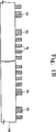
Wie in 1A und 1B gezeigt, kann eine Flash-Speichervorrichtung eine Mehrzahl von parallelen aktiven Bereichen ACT in einem Halbleitersubstrat enthalten, die durch Vorrichtungsisolierschichten getrennt sind. Zusätzlich können Masseauswahlleitungen GSL, Reihenauswahlleitungen SSL und Wortleitungen WL die aktiven Bereiche ACT kreuzen. Insbesondere kann ein jeweiliges Ladungsspeichergate zwischen jeder Wortleitung WL und jedem aktiven Bereich ACT vorgesehen sein zum Bereitstellen einer jeweiligen Speicherzelle an jeder Überschneidung einer Wortleitung WL mit einem aktiven Bereich ACT. Darüber hinaus kann eine Mehrzahl von Speicherzellen entlang eines aktiven Bereiches ACT zwischen einer Masseauswahlleitung GSL und einer Reihenauswahlleitung SSL eine Speicherzellenreihe definieren. Wie weiter in 1A und 1B gezeigt, können benachbarte Speicherzellenreihen durch zwei Masseauswahlleitungen GSL oder durch zwei Reihenauswahlleitungen SSL getrennt sein.As in 1A and 1B As shown, a flash memory device may include a plurality of parallel active regions ACT in a semiconductor substrate separated by device isolation layers. In addition, ground select lines GSL, row select lines SSL and word lines WL may cross the active areas ACT. In particular, a respective charge storage gate may be provided between each word line WL and each active area ACT for providing a respective memory cell at each intersection of a word line WL with an active area ACT. Moreover, a plurality of memory cells along an active area ACT between a ground select line GSL and a row select line SSL may define a memory cell row. As in further 1A and 1B As shown, adjacent memory cell rows may be separated by two ground select lines GSL or by two row select lines SSL.
Wie in den vergrößerten Querschittsansichten aus 1C und 1D gezeigt, kann eine Gateisolierschicht GIL zwischen der Masseauswahlleitung GSL und dem aktiven Bereich ACT des Halbleitersubstrates SUB vorgesehen sein. Zusätzlich kann ein Ladungsspeichergate CSG zwischen der Wortleitung WL1 und dem aktiven Bereich ACT des Substrates SUB vorgesehen sein, kann eine Tunnelisolierschicht TIL zwischen dem Ladungsspeichergate CSG und dem aktiven Bereich ACT vorgesehen sein, und kann eine Barrierenisolierschicht BIL zwischen dem Ladungsspeichergate CSG und der Wortleitung WL1 vorgesehen sein.As in the enlarged cross section views 1C and 1D As shown, a gate insulating film GIL may be provided between the ground select line GSL and the active region ACT of the semiconductor substrate SUB. In addition, a charge storage gate CSG may be provided between the word line WL1 and the active area ACT of the substrate SUB, a tunnel insulating layer TIL may be provided between the charge storage gate CSG and the active area ACT, and a barrier insulating layer BIL may be provided between the charge storage gate CSG and the word line WL1 be.
Während eines Programmiervorgangs (für eine andere Speicherzelle als die in 1C gezeigte) können 0 Volt an die Masseauswahlleitung GSL angelegt sein und kann eine Durchgangsspannung Vpass an die nicht-ausgewählte Wortleitung WL1 angelegt sein, wie in 1C gezeigt ist. Zusätzlich kann eine Programmierspannung Vpgm an eine ausgewählte Wortleitung (nicht dargestellt) angelegt sein, welche einer zu programmierenden Speicherzelle (zu programmierenden Speicherzellen) entspricht. Eine Gate-Spannung des Masseauswahltransistors (der durch die Masseauswahlleitung GSL und die Gateisolierschicht GIL definiert ist) kann somit 0 Volt sein, während eine Drain-Spannung des Masseauswahltransistors etwa 10 Volt sein kann, was zu einem von einem Gate indizierten Leckstrom GIDL führt.During a programming operation (for a memory cell other than the one in 1C 0 volts may be applied to the ground select line GSL, and a continuity voltage Vpass may be applied to the unselected word line WL1 as shown in FIG 1C is shown. In addition, a program voltage Vpgm may be applied to a selected word line (not shown) corresponding to a memory cell to be programmed (memory cells to be programmed). Thus, a gate voltage of the ground select transistor (defined by the ground select line GSL and gate insulating layer GIL) may be 0 volts, while a drain voltage of the ground select transistor may be about 10 volts, resulting in a gate current leakage current GIDL.
Während eines Löschvorgangs kann der Masseauswahlleitung GSL ermöglicht werden, zu schweben, und eine Löschspannung Vers von etwa 20 Volt kann an eine p-Wanne des Substrates SUB angelegt werden, und 0 Volt können an die Wortleitung WL1 angelegt werden, wie in 1D gezeigt. Dementsprechend kann die an die p-Wanne angelegte Löschspannung Vers von 20 Volt ein Potential der Masseauswahlleitung GSL erhöhen, und ein Potential des Ladungsspeichergates CSG (benachbart zu der Masseauswahlleitung GSL) kann aufgrund der kapazitiven Kopplung Cp zwischen der Masseauswahlleitung GSL und dem Ladungsspeichergate CSG ansteigen. Eine ungewünschte Löschstörung kann somit an dem Ladungsspeichergate CSG und/oder der Wortleitung WL1 resultieren.During an erase operation, ground select line GSL may be allowed to float, and an erase voltage vers of about 20 volts may be applied to a p-well of substrate SUB, and 0 volts may be applied to word line WL1, as in FIG 1D shown. Accordingly, the erase voltage V s applied to the p-well can increase a potential of the ground select line GSL, and a potential of the charge storage gate CSG (adjacent to the ground select line GSL) may vary due to the capacitive coupling Cp between the ground select line GSL and the Charge storage rate CSG increase. An undesired erase fault can thus result at the charge storage gate CSG and / or the word line WL1.
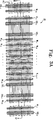
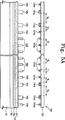
2A ist eine Draufsicht einer nicht-flüchtigen Speichervorrichtung 20 (wie z. B. einer Flash-Speichervorrichtung) gemäß einigen Ausführungsformen der vorliegenden Erfindung, und 2B ist eine Querschnittsansicht entlang Schnittlinie II-II' aus 2A. Die Flash-Speichervorrichtung 20, kann eine Mehrzahl von parallelen aktiven Bereichen ACT in einem Halbleitersubstrat SUB getrennt durch Vorrichtungsisolierschichten enthalten. Zusätzlich können Masseauswahlleitungen GSL0-2, Reihenauswahlleitungen SSL0-2, Dummy-Wortleitungen WLd und Speicherzellen-Wortleitungen WL1-2n (wobei n eine ganze Zahl ist) die aktiven Bereiche ACT kreuzen. Insbesondere kann ein jeweiliges Ladungsspeichergate zwischen jeder Speicherzellen-Wortleitung WL1-2n und jedem aktiven Bereich ACT vorgesehen sein, um eine jeweilige Speicherzelle an jeder Überschneidung einer Speicherzellen-Wortleitung WL1-2n mit einem aktiven Bereich ACT bereitzustellen. Genauso kann ein Ladungsspeichergate zwischen jeder Dummy-Wortleitung WLd und dem aktiven Bereich ACT vorgesehen sein, so dass die Strukturen der Dummy-Wortleitungen WLd und der Speicherzellen-Wortleitungen WL1-2n die gleichen sind. 2A Fig. 10 is a plan view of a non-volatile memory device 20 (such as a flash memory device) according to some embodiments of the present invention, and 2 B is a cross-sectional view along section line II-II 'from 2A , The flash memory device 20 , a plurality of parallel active regions ACT may be included in a semiconductor substrate SUB separated by device insulating layers. In addition, ground select lines GSL 0-2 , row select lines SSL 0-2 , dummy word lines WL d, and memory cell word lines WL 1-2n (where n is an integer) may cross the active areas ACT. In particular, a respective charge storage gate may be provided between each memory cell word line WL 1-2n and each active area ACT to provide a respective memory cell at each intersection of a memory cell word line WL 1-2n with an active area ACT. Similarly, a charge storage gate may be provided between each dummy word line WL d and the active area ACT, so that the structures of the dummy word lines WL d and the memory cell word lines WL 1-2n are the same.
Eine gerade Anzahl von Speicherzellen-Wortleitungen WL1-2n entlang eines aktiven Bereichs ACT zwischen einer Masseauswahlleitung GSL und einer Reihenauswahlleitung SSL (z. B. zwischen GSL1 und SSL1) kann eine Speicherzellenreihe mit einer geraden Anzahl an Speicherzellen definieren. Wie weiter in den 2A–B gezeigt ist, können benachbarte Speicherzellen-Reihen durch zwei Masseauswahlleitungen GSL (z. B. GSL0 und GSL1) oder durch zwei Reihenauswahlleitungen SSL (z. B. SSL1 und SSL2) getrennt sein. Genauer können 2k (wobei k eine positive ganze Zahl ist) Speicherzellen-Wortleitungen WL1-2n eine Speicherzellenreihe mit 2k zum Speichern von Daten verwendeten Speicherzellen definieren. Die Dummy-Wortleitung WLd wird jedoch nicht zum Speichern von Daten verwendet.An even number of memory cell word lines WL 1-2n along an active area ACT between a ground select line GSL and a row select line SSL (eg, between GSL 1 and SSL 1 ) may define a memory cell array having an even number of memory cells. As further in the 2A - B, adjacent memory cell rows may be separated by two ground select lines GSL (eg GSL 0 and GSL 1 ) or by two row select lines SSL (eg SSL 1 and SSL 2 ). More specifically can 2 k (where k is a positive integer) memory cell word lines WL 1-2n define a row of memory cells with 2 k used for storing data memory cells. However, the dummy word line WL d is not used for storing data.
Darüber hinaus kann eine Anordnung von Speicherzellen-Wortleitungen WL1-2n und einer Dummy-Wortleitung WLd von benachbarten Speicherzellen-Reihen eine Spiegelsymmetrie aufweisen. Z. B. kann eine Anordnung von Speicherzellen-Wortleitungen WL1-2n und Dummy-Wortleitungen WLd zwischen der Masseauswahlleitung GSL0 und der Reihenauswahlleitung SSL0 Spiegelsymmetrie relativ zu einer Anordnung von Speicherzellen-Wortleitungen WL1-2n und der Dummy-Wortleitung WLd zwischen der Masseauswahlleitung GSL1 und der Reihenauswahlleitung SSL1 besitzen. Genauso kann eine Anordnung von Speicherzellen-Wortleitungen WL1-2n und der Dummy-Wortleitung WLd zwischen der Masseauswahlleitung GSL1 und der Reihenauswahlleitung SSL1 Spiegelsymmetrie relativ zu einer Anordnung von Speicherzellen-Wortleitungen WL1-2n und der Dummy-Wortleitung WLd zwischen der Masseauswahlleitung GSL2 und der Reihenauswahlleitung SSL2 besitzen.In addition, an array of memory cell word lines WL 1-2n and a dummy word line WL d of adjacent memory cell rows may have mirror symmetry. For example, an array of memory cell word lines WL 1-2n and dummy word lines WL d between ground select line GSL 0 and row select line SSL 0 may have mirror symmetry relative to an array of memory cell word lines WL 1-2n and dummy word line WL d between Mass selection line GSL 1 and the series selection line SSL 1 own. Similarly, an arrangement of memory cell word lines WL 1-2n and dummy word line WL d between ground select line GSL 1 and row select line SSL 1 may mirror symmetry relative to an array of memory cell word lines WL 1-2n and dummy word line WL d the ground selection line GSL 2 and the row selection line SSL 2 have.
Durch Vorsehen einer Dummy-Wortleitung WLd zwischen einer Masseauswahlleitung GSL und einer ersten Speicherzellen-Wortleitung WL1 einer Speicherzellen-Reihe kann ein masseinduzierter Leckstrom und/oder eine Löschstörung an der ersten Speicherzellen-Wortleitung WL1 verringert werden. Darüber hinaus kann ein Controller der nicht-flüchtigen Speichervorrichtung an die Masseauswahlleitungen, die Reihenauswahlleitungen, die Speicherzellen-Wortleitungen und die Dummy-Wortleitungen angeschlossen sein. Während eines Löschvorgangs kann der Controller z. B. derart konfiguriert sein, dass er den Masseauswahlleitungen GSL1 ermöglicht, zu schweben, dass er eine Löschspannung Vers von etwa 20 Volt an eine p-Wanne des Substrates SUB anlegt und dass er 0 Volt an die Speicherzellen-Wortleitungen WL1-2n anlegt. Zusätzlich kann der Controller derart konfiguriert sein, dass er eine Vorspannung Vb an die Dummy-Wortleitung WLd anlegt, wobei die Vorspannung Vb zwischen einer Versorgungsspannung Vcc und einer Durchgangsspannung Vpass ist (d. h. Vcc < Vb < Vpass), um dadurch eine Löschstörung bei der ersten Speicherzellen-Wortleitung WL1 und/oder bei jeweiligen Ladungssspeicherschichten zu verringert.By providing a dummy word line WL d between a ground select line GSL and a first memory cell word line WL 1 of a memory cell row, a ground-induced leakage current and / or an erase fault on the first memory cell word line WL 1 can be reduced. Moreover, a controller of the nonvolatile memory device may be connected to the ground select lines, the row select lines, the memory cell word lines, and the dummy word lines. During an erase operation, the controller z. B. configured to enable the ground select lines GSL 1 to float applying an erase voltage vers of about 20 volts to a p-well of the substrate SUB and to apply 0 volts to the memory cell word lines WL 1-2n , In addition, the controller may be configured to apply a bias voltage Vb to the dummy word line WL d , where the bias voltage Vb is between a supply voltage Vcc and a pass voltage Vpass (ie, Vcc <Vb <Vpass) to thereby provide an erase fault in the first memory cell word line WL 1 and / or reduced at respective charge storage layers.
Während eines Schreib-(oder Programmier-)Vorgangs kann der Controller derart konfiguriert sein, dass er die Versorgungsspannung Vcc an die Masseauswahlleitung GSL1 anlegt, dass er 0 Volt an eine p-Wanne des Substrates SUB anlegt, dass er eine Durchgangsspannung Vpass an die nicht-ausgewählten Wortleitungen anlegt, und dass er eine Programmierspannung Vpgm an die ausgewählte Wortleitung anlegt. Zusätzlich kann der Controller derart konfiguriert sein, dass er eine Vorspannung Vd an die Dummy-Wortleitung WLd anlegt, wobei die Vorspannung Vb zwischen der Versorgungsspannung Vcc und der Durchgangsspannung Vpass ist (d. h. Vcc < Vbc < Vpass), um dadurch den von Masse induzierten Leckstrom bei der zu der Dummy-Wortleitung benachbarten Masseauswahlleitung zu verringern.During a write (or program) operation, the controller may be configured to apply the supply voltage Vcc to the ground select line GSL 1 , to apply 0 volts to a p-well of the substrate SUB, to apply a pass voltage Vpass to the applying undelected word lines, and applying a programming voltage Vpgm to the selected word line. In addition, the controller may be configured to apply a bias voltage Vd to the dummy word line WL d , where the bias voltage Vb between the supply voltage Vcc and the through voltage is Vpass (ie, Vcc <Vbc <Vpass) thereby to be ground-induced To reduce leakage current at the adjacent to the dummy word line ground selection line.
Wie in den 2A–B gezeigt können die Dummy-Wortleitung WLd und jede der Speicherzellen-Wortleitungen WL1 bis WL2n etwa eine gleiche Breite F1 haben. Zusätzlich kann etwa eine gleiche Weite/ein gleicher Abstand W1 eine Gateauswahlleitung GSL und eine benachbarte Dummy-Wortleitung WLd trennen, kann etwa die gleiche Weite/der gleichen Abstand W1 eine Dummy-Wortleitung WLd und eine benachbarte erste Speicherzellen-Wortleitung WL1 trennen, kann etwa die gleiche Weite/der gleiche Abstand W1 benachbarte Speicherzellen-Wortleitungen WLx und WLx+1 trennen, und kann etwa die gleiche Weite/der gleiche Abstand W1 eine letzte Speicherzellen-Wortleitung WL2n und eine benachbarte Reihenauswahlleitung SSL trennen. Darüber hinaus können die Weiten F1 und W1 etwa gleich sein und insbesondere kann jede der Weiten F1 und W1 etwa ein Viertel (1/4) einer Periode P1 sein, die durch benachbarte gerade Speicherzellen-Wortleitungen WLgerade und WLgerade+2 (d. h. gerade Speicherzellen-Wortleitungen, die durch nur eine ungerade Speicherzellen-Wortleitung getrennt sind) definiert ist oder durch benachbarte ungerade Speicherzellen-Wortleitungen WLumgerade und WLumgerade+2 (d. h. ungerade Speicherzellen-Wortleitungen, die durch nur eine gerade Speicherzellen-Wortleitung getrennt sind) definiert ist. Wie weiter in den 2A–B gezeigt ist können benachbarte Masseauswahlleitungen GSL0 und GSL1 durch etwa eine Weite/einen Abstand W2 getrennt sein, und können benachbarte Reihenauswahlleitungen SSL0 und SSL1 durch etwa die gleiche Weite/den gleichen Abstand W2 getrennt sein. Die Weite/der Abstand W2 kann zumindest etwa 3 Mal größer als die Weite/der Abstand W1 sein.As in the 2A 3B, the dummy word line WL d and each of the memory cell word lines WL 1 to WL 2n may be approximately equal in width F 1 . In addition, about a same width / spacing W 1 may separate a gate select line GSL and an adjacent dummy word line WL d , approximately the same width / spacing W 1 may include a dummy word line WL d and an adjacent first memory cell word line WL 1 , can be about the same width / the the same distance W 1 separate adjacent memory cell word lines WL x and WL x + 1 , and approximately the same width / spacing W 1 may separate one last memory cell word line WL 2n and an adjacent row select line SSL. Moreover, the widths F 1 and W 1 may be approximately equal and, in particular, each of the widths F 1 and W 1 may be about one quarter (1/4) of a period P 1 that is even and WL even by adjacent even memory cell word lines WL +2 (ie even memory cell word lines, which are separated by only an odd memory cell word line) is defined or umgerade by adjacent odd memory cell word lines WL and WL umgerade + 2 (ie, odd memory cell word lines by only an even memory cell Word line are separated) is defined. As further in the 2A B-B, adjacent ground select lines GSL 0 and GSL 1 may be separated by approximately one width W 2 , and adjacent row select lines SSL 0 and SSL 1 may be separated by approximately the same width / distance W 2 . The width W 2 may be at least about 3 times larger than the width W 1 .
Jede Speicherzellen-Wortleitung WL1 bis WL2n kann somit eine jeweilige Steuerelektrode für eine nichtflüchtige Speicherzelle (wie z. B. eine Flash-Speicherzelle) einer Speicherzellen-Reihe auf einem gleichen aktiven Bereich ACT zwischen einer Masseauswahlleitung (z. B. GSL1) und einer Reihenauswahlleitung (z. B. SSL1) bereitstellen. Jede nichtflüchtige Speicherzelle kann außerdem eine Ladungsspeicherschicht zwischen der jeweiligen Speicherzellen-Wortleitung und dem aktiven Bereich, eine Tunnelisolierschicht zwischen dem aktiven Bereich und der Ladungsspeicherschicht sowie eine Barrierenisolierschicht zwischen der Speicherzellen-Wortleitung und der Ladungsspeicherschicht enthalten.Each memory cell word line WL 1 to WL 2n may thus have a respective control electrode for a nonvolatile memory cell (such as a flash memory cell) of a memory cell array on a same active area ACT between a ground select line (eg, GSL 1 ). and a row select line (e.g., SSL 1 ). Each non-volatile memory cell may further include a charge storage layer between the respective memory cell word line and the active region, a tunnel insulating layer between the active region and the charge storage layer, and a barrier insulating layer between the memory cell word line and the charge storage layer.
Jede Dummy-Wortleitung WLd kann einen Aufbau haben, der gleich wie der oben diskutierte mit Bezug auf die Speicherzellen-Wortleitungen ist (mit einer Tunnelisolierschicht, einer Ladungsspeicherschicht und einer Barrierenisolierschicht zwischen jeder Dummy-Wortleitung und jeweiligen aktiven Bereichen). Die Dummy-Zellwortleitungen (und verknüpfte Tunnelisolierschichten, Ladungsspeicherschichten sowie Barriereisolierschichten) werden jedoch nicht zum Speichern von Daten verwendet, sondern sind stattdessen vorgesehen zum Verringern von masseinduziertem Leckstrom an benachbarten Masseauswahlleitungen während Programmiervorgängen und/oder zum Verringern der Löschvorspannung an den benachbarten Speicherzellen während der Löschvorgänge.Each dummy word line WL d may have a construction similar to that discussed above with respect to the memory cell word lines (having a tunnel insulating layer, a charge storage layer, and a barrier insulating layer between each dummy word line and respective active regions). However, the dummy cell word lines (and associated tunnel insulating layers, charge storage layers, and barrier insulating layers) are not used to store data, but instead are designed to reduce bulk induced leakage current on adjacent ground select lines during programming operations and / or to reduce the erase bias on the adjacent memory cells during erase operations ,
Das Muster der Masseauswahlleitungen GSL, der Dummy-Wortleitungen WLd, der Speicherzellen-Wortleitungen WL1 bis WL2n und der Reihenauswahlleitungen SSL kann gebildet werden unter Verwendung von selbstausgerichteter Doppelmusterung, wie sie unten genauer diskutiert wird. Z. B. können die Masseauswahlleitungen GSL, die Reihenauswahlleitungen SSL und die ungeraden Speicherzellen-Wortleitungen (WL1, WL3, WL5, ..., WL2n-1) gebildet werden entsprechend einem Muster einer Fotolithographiemaske, und können die Dummy-Wortleitungen WLd und die geraden Speicherzellen-Wortleitungen (WL2, WL4, WL6, ..., WL2n) gebildet werden unter Verwendung selbstausgerichteter Doppelmusterung.The pattern of the ground select lines GSL, the dummy word lines WL d , the memory cell word lines WL 1 to WL 2n, and the row selection lines SSL may be formed using self-aligned double patterning as discussed in more detail below. For example, the ground selection lines GSL, the row selection lines SSL and the odd memory cell word lines (WL 1 , WL 3 , WL 5 , ..., WL 2n-1 ) may be formed according to a pattern of a photolithography mask, and the dummy word lines WL d and the even memory cell word lines (WL 2 , WL 4 , WL 6 , ..., WL 2n ) are formed using self-aligned double patterning.
Gemäß einigen Ausführungsformen der vorliegenden Erfindung, die in den 2A–B dargestellt sind, kann eine erste Speicherzellen-Reihe auf dem aktiven Bereich (ACT) eine erste Mehrzahl von Speicherzellen-Wortleitungen WL1 bis WL2n enthalten, die den aktiven Bereich ACT zwischen der ersten Masseauswahlleitung GSL1 und der ersten Reihenauswahlleitung SSL1 kreuzen, und etwa ein gleicher erster Abstand W1 kann vorgesehen sein zwischen benachbarten der ersten Mehrzahl von Wortleitungen. Zusätzlich kann eine zweite Speicherzellen-Reihe auf dem aktiven Bereich ACT eine zweite Mehrzahl von Wortleitungen WL1 bis WL2n enthalten, die den aktiven Bereich ACT zwischen einer zweiten Masseauswahlleitung GSL0 und einer zweiten Reihenauswahlleitung SSL1 kreuzen, und etwa der gleiche erste Abstand WL1 kann vorgesehen sein zwischen benachbarten der zweiten Mehrzahl von Wortleitungen. Genauer kann die erste Masseauswahlleitung GSL1 zwischen der zweiten Masseauswahlleitung GSL0 und der ersten Mehrzahl von Wortleitungen sein, und die zweite Masseauswahlleitung GSL0 kann zwischen der ersten Masseauswahlleitung GSL1 und der zweiten Mehrzahl von Wortleitungen sein. Darüber hinaus können Abschnitte des aktiven Bereichs ACT zwischen der ersten und der zweiten Masseauswahlleitung GSL1 und GSL0 frei von Wortleitungen sein, und der zweite Abstand W2 zwischen der ersten und der zweiten Masseauswahlleitung GSL1 und GSL0 können zumindest etwa dreimal größer als der erste Abstand W1 sein. Z. B. kann der zweite Abstand W2 zwischen etwa drei bis viermal größer als der erste Abstand W1 sein, und genauer kann der zweite Abstand W2 mehr als dreimal größer als der erste Abstand W1 und insbesondere mehr als viermal größer als der erste Abstand W1 sein.According to some embodiments of the present invention, which are incorporated in the 2A 1B, a first memory cell row on the active area (ACT) may include a first plurality of memory cell word lines WL 1 to WL 2n crossing the active area ACT between the first ground select line GSL 1 and the first row select line SSL 1 , And about a same first distance W 1 may be provided between adjacent ones of the first plurality of word lines. In addition, a second memory cell row on the active area ACT may include a second plurality of word lines WL 1 to WL 2n crossing the active area ACT between a second ground select line GSL 0 and a second row select line SSL 1 , and about the same first distance WL 1 may be provided between adjacent ones of the second plurality of word lines. Specifically, the first ground select line GSL 1 may be between the second ground select line GSL 0 and the first plurality of word lines, and the second ground select line GSL 0 may be between the first ground select line GSL 1 and the second plurality of word lines. In addition, portions of the active region ACT between the first and second ground selection lines GSL 1 and GSL 0 may be free of word lines, and the second distance W 2 between the first and second ground selection lines GSL 1 and GSL 0 may be at least about three times larger than that be first distance W 1 . For example, the second distance W 2 may be between about three to four times greater than the first distance W 1 , and more specifically, the second distance W 2 may be more than three times greater than the first distance W 1 and in particular more than four times greater than the first distance W Be 1 .
Zusätzlich kann die Dummy-Wortleitung WLd zwischen der ersten Speicherzellen-Wortleitung WL1 und der ersten Masseauswahlleitung GSL1 sein, und etwa der gleiche erste Abstand W1 kann zwischen der ersten Masseauswahlleitung GSL1 und der Dummy-Wortleitung WLd vorgesehen sein. Etwa der gleiche erste Abstand W1 kann außerdem vorgesehen sein zwischen der Dummy-Wortleitung WLd und der ersten Speicherzellen-Wortleitung WL1 sowie zwischen der letzten Speicherzellen-Wortleitung WL2n-1 und der Reihenauswahlleitung SSL1.In addition, the dummy word line WL d may be between the first memory cell word line WL 1 and the first ground select line GSL 1 , and approximately the same first distance W 1 may be provided between the first ground select line GSL 1 and the dummy word line WL d . About the same first distance W 1 can also be provided between the dummy word line WL d and the first memory cell word line WL 1 and between the last memory cell word line WL 2n-1 and the row selection line SSL 1 .
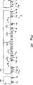
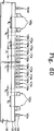
Die 5A–D sind Querschnittsansichten, die Arbeitsschritte des Bildens der nichtflüchtigen Speicherstrukturen aus den 2A–B unter Verwendung selbstausgerichteter Doppelmusterung gemäß einigen Ausführungsformen der vorliegenden Erfindung darstellen. Wie in 5A gezeigt kann ein Substrat 50 eine Ätzzielschicht 52 darauf enthalten, und kann die Ätzzielschicht 52 Schichten der Materialien beinhalten, die zum Bilden der Speicherzellen, Wortleitungen, Auswahltransistoren und Auswahlleitungen aus 2A–B verwendet werden.The 5A D are cross-sectional views illustrating the operations of forming the nonvolatile memory structures from FIGS 2A B using self aligned dual pattern according to some embodiments of the present invention. As in 5A a substrate can be shown 50 an etching target layer 52 contained on it, and can the etching target layer 52 Layers of materials include those used to form the memory cells, word lines, select transistors, and select lines 2A -B be used.
Genauer kann die Zielschicht eine Tunnelisolierschicht (wie Z. B. eine Schicht aus Siliziumoxid), eine Ladungsspeichergateschicht (wie z. B. eine Schicht aus Polysilizium oder Siliziumnitrid), eine Barrierenisolierschicht (wie z. B. eine Schicht aus Siliziumoxid oder einem anderen dielektrischen Material, das verschieden von der Ladungsspeichergateschicht ist) sowie eine leitfähige Schicht (wie z. B. eine Schicht aus Polysilizium und/oder Metall) enthalten. Die Ladungsspeicherschicht kann zwischen der leitfähigen Schicht und dem Substrat sein, wobei die Tunnelisolierschicht die Ladungsspeicherschicht und das Substrat trennt und wobei die Barrierenisolierschicht die Ladungsspeicherschicht und die leitfähige Schicht trennt. Zusätzlich kann eine erste Hartmaskenschicht 55 auf der Ätzzielschicht 52 ausgebildet werden, und die erste Hartmaskenschicht 55 kann eine Siliziumnitridschicht 56 auf einer Pad-Oxidschicht 54 enthalten.Specifically, the target layer may be a tunnel insulating layer (such as a layer of silicon oxide), a charge storage gate layer (such as a layer of polysilicon or silicon nitride), a barrier insulating layer (such as a layer of silicon oxide or other dielectric material, e.g. different from the charge storage gate layer) as well as a conductive layer (such as a layer of polysilicon and / or metal). The charge storage layer may be between the conductive layer and the substrate, wherein the tunnel insulating layer separates the charge storage layer and the substrate, and wherein the barrier insulating layer separates the charge storage layer and the conductive layer. In addition, a first hard mask layer 55 on the etching target layer 52 are formed, and the first hard mask layer 55 may be a silicon nitride layer 56 on a pad oxide layer 54 contain.
Eine Fotolackschicht auf der ersten Hartmaskenschicht 55 kann unter Verwendung der Fotomaske 100 derart gemustert werden, dass das Fotolackmuster 58 mit ungeraden Wortleitungs-Fotolackmustern 58w, Masseauswahlleitungs-Fotolackmustern 58g und Reihenauswahlleitungs-Fotolackmustern 58s bereitgestellt wird. Genauer enthält die Fotomaske 100 ein Fotomaskenmuster 104 auf einem transparenten Substrat 102. Das Fotomaskenmuster 104 kann ungerade Wortleitungs-Fotomaskenmuster 104w, die den ungeraden Wortleitungs-Fotolackmustern 58w entsprechen, Masseauswahlleitungs-Fotomaskenmuster 104g, die den Masseauswahlleitungs-Fotolackmustern 58g entsprechen, sowie Reihenauswahlleitungs-Fotomaskenmuster 104s, die den Reihenauswahlleitungs-Fotolackmustern 58s entsprechen, enthalten.A photoresist layer on the first hardmask layer 55 can using the photomask 100 be patterned such that the photoresist pattern 58 with odd word line photoresist patterns 58w , Earth selection line photoresist patterns 58g and row selection line photoresist patterns 58s provided. More precisely contains the photomask 100 a photomask pattern 104 on a transparent substrate 102 , The photomask pattern 104 may have odd wordline photomask patterns 104w representing the odd word line photoresist patterns 58w Corresponds to ground selection photo-mask pattern 104g picking up the ground array photo resist patterns 58g and row select line photomask patterns 104s patterning the row selection line photoresist 58s correspond, included.
Wie weiter in 5A gezeigt, können benachbarte ungerade Wortleitungs-Fotomaskenmuster 104w voneinander um etwa eine Weite/einen Abstand W11 beabstandet sein, und können benachbarte ungerade Wortleitungs-Fotolackmuster 58w um etwa die Weite/den Abstand W11 voneinander beabstandet sein. Ein erstes der ungeraden Wortleitungs-Fotomaskenmuster 104w kann von einem benachbarten Masseauswahlleitungs-Fotomaskenmuster 104g um etwa die Weite/den Abstand W11 beabstandet sein, und ein letztes der ungeraden Wortleitungs-Fotomaskenmuster 104w kann von einem benachbarten Reihenauswahlleitungs-Fotomaskenmuster 104s um etwa die Weite/den Abstand W11 beabstandet sein. Genauso kann ein erstes der ungeraden Wortleitungs-Fotolackmuster 58w von einem benachbarten Masseauswahlleitungs-Fotolackmuster 58g um etwa die Weite/den Abstand W11 beabstandet sein, und kann ein letztes der ungeraden Wortleitungs-Fotomaskenmuster 58w von einem benachbarten Reihenauswahlleitungs-Fotomaskenmuster 58s um etwa die Weite/den Abstand W11 beabstandet sein.As in further 5A may show adjacent odd word line photomask patterns 104w be spaced apart by about a distance W 11 , and may have adjacent odd word line photoresist patterns 58w be spaced apart by about the width / distance W 11 . A first of the odd wordline photomask patterns 104w may be from an adjacent ground select line photomask pattern 104g by about the distance W 11 and a last one of the odd word line photomask patterns 104w may be from an adjacent row select line photomask pattern 104s be spaced by about the width / distance W 11 . Likewise, a first of the odd word line photoresist patterns may be used 58w from an adjacent ground select line photoresist pattern 58g may be spaced by about the distance W 11 , and may be a last one of the odd word line photomask patterns 58w from an adjacent row select line photomask pattern 58s be spaced by about the width / distance W 11 .
Darüber hinaus kann jedes der ungeraden Wortleitungs-Fotomaskenmuster 104w und jedes der ungeraden Wortleitungs-Fotolackmuster 58w eine Breite von etwa F1 haben, und die Weite/der Abstand W11 kann etwa das dreifache der Breite F1 sein. Zusätzlich können benachbarte der ungeraden Wortleitungs-Fotomaskenmuster 104w und benachbarte der ungeraden Wortleitungs-Fotolackmuster 58w eine Periode P1 definieren, und die Periode P1 kann etwa das Vierfache der Breite F1 sein. Die Breite F1 kann eine minimale Strukturgröße sein, die bei der verwendeten Fotolithographietechnik verfügbar ist. Benachbarte Masseauswahlleitungs-Fotomaskenmuster 104g, benachbarte Reihenauswahlleitungs-Fotomaskenmuster 104s, benachbarte Masseauswahlleitungs-Fotolackmuster 58g sowie benachbarte Reihenauswahlleitungs-Fotolackmuster 58s können durch eine Weite/einen Abstand W2 voneinander getrennt sein, und die Weite/der Abstand W2 kann größer als das Vierfache der Breite F1 sein. Darüber hinaus kann der zweite Abstand W2 zumindest dreimal größer als der erste Abstand W1 sein. Z. B. kann der zweite Abstand W2 zwischen etwa drei und viermal größer als der erste Abstand W1 sein, und insbesondere kann der zweite Abstand W2 dreimal größer als der erste Abstand W1 sein, und noch genauer, mehr als viermal größer als der erste Abstand W1.In addition, each of the odd word line photomask patterns 104w and each of the odd wordline photoresist patterns 58w have a width of about F 1 , and the width / distance W 11 may be about three times the width F 1 . In addition, adjacent ones of the odd word line photomask patterns may be used 104w and adjacent the odd word line photoresist patterns 58w define a period P 1 , and the period P 1 may be about four times the width F 1 . The width F 1 may be a minimum feature size available in the photolithography technique used. Neighboring ground selection line photomask patterns 104g adjacent row select line photomask patterns 104s , neighboring ground selection line photoresist patterns 58g and adjacent row select line photoresist patterns 58s may be separated by a width W 2 , and the width W 2 may be greater than four times the width F 1 . In addition, the second distance W 2 may be at least three times greater than the first distance W 1 . For example, the second distance W 2 may be between about three and four times greater than the first distance W 1 , and in particular, the second distance W 2 may be three times greater than the first distance W 1 , and more specifically, more than four times greater than the first distance W 2 Distance W 1 .
Genauer kann eine durchgehende Fotolackschicht durch die Fotomaske 100 hindurch selektiv Strahlung ausgesetzt und dann entwickelt werden zum Bereitstellen des Fotolackmusters 58 aus 5A. Dementsprechend wird eine Anordnung des Fotolackmusters 58 durch eine Anordnung des Fotomaskenmusters 104 definiert. Zusätzlich entspricht das Fotolackmuster 58 einem Muster von Gateauswahlleitungen, Reihenauswahlleitungen und ungeraden Wortleitungen, die oben mit Bezug auf die 2A–B diskutiert wurden.More specifically, a continuous photoresist layer may pass through the photomask 100 be selectively exposed to radiation and then developed to provide the photoresist pattern 58 out 5A , Accordingly, an arrangement of the resist pattern becomes 58 by an arrangement of the photomask pattern 104 Are defined. In addition, the photoresist pattern corresponds 58 a pattern of gate select lines, row select lines, and odd word lines described above with respect to FIGS 2A -B were discussed.
Abschnitte der ersten Hartmaskenschicht 55 (mit der Siliziumnitridschicht 56 und der Pad-Oxidschicht 54), die durch das Fotolackmuster 58 freigelegt sind, können selektiv entfernt werden (z. B. durch Trockenätzen) zum Bereitstellen eines ersten Hartmaskenmusters 60 (mit Masseauswahlleitungs-Hartmaskenmustern 60g, Reihenauswahlleitungs-Hartmaskenmustern 60s und ungeraden Wortleitungs-Hartmaskenmustern 60w), wie in 5B gezeigt ist. Wenn die erste Hartmaskenschicht 55 separate Schickten 54 und 56 enthält, kann jedes Element des ersten Hartmaskenmusters 60 auch separate Schichten 54 und 56 enthalten. Etwa ein gleicher Abstand/eine gleiche Weite W11 kann vorgesehen sein zwischen einem Masseauswahlleitungs-Hartmaskenmuster 60g und einem ersten ungeraden Wortleitungs-Hartmaskenmuster 60w, zwischen benachbarten ungeraden Wortleitungs-Hartmaskenmustern 60w, sowie zwischen einem letzten ungeraden Wortleitungs-Hartmaskenmuster 60w und einem Reihenauswahlleitungs-Hartmaskenmuster 60s. Jedes Element des ersten Hartmaskenmusters 60 kann eine Schicht aus Siliziumnitrid und/oder Siliziumoxid enthalten. Nach dem selektiven Entfernen von Abschnitten der ersten Hartmaskenschicht kann das Fotolackmuster 58 entfernt werden.Sections of the first hard mask layer 55 (with the silicon nitride layer 56 and the pad oxide 54 ) passing through the photoresist pattern 58 can be selectively removed (eg, by dry etching) to provide a first hard mask pattern 60 (with ground selection hardmask patterns 60g , Row selection line hard mask patterns 60s and odd wordline hardmask patterns 60w ), as in 5B is shown. When the first hard mask layer 55 separate send 54 and 56 can contain any element of the first hardmask pattern 60 also separate layers 54 and 56 contain. Approximately an equal distance / an equal width W 11 may be provided between a ground select line hard mask pattern 60g and a first odd wordline hardmask pattern 60w , between adjacent odd word line hardmask patterns 60w , as well as between a last odd word line hard mask pattern 60w and a row select line hard mask pattern 60s , Each element of the first hardmask pattern 60 may contain a layer of silicon nitride and / or silicon oxide. After selectively removing portions of the first hardmask layer, the photoresist pattern may 58 be removed.
Wie weiter in 5B gezeigt kann eine Opfermaskenschicht 62 auf dem ersten Hartmaskenmuster 60 und auf Abschnitten der Ätzzielschicht 52 gebildet werden, die durch das erste Hartmaskenmuster 60 freilgelegt sind, und die Opfermaskenschicht 62 und das erste Hartmaskenmuster 60 können verschiedene Materialien umfassen. Z. B. können obere Schichten 56 des ersten Hartmaskenmusters 60 eine Schicht aus Siliziumnitrid sein, und die Opfermaskenschicht 62 kann eine Schicht aus Polysilizium sein. Darüber hinaus kann eine Dicke der Opfermaskenschicht 62 derart bereitgestellt werden, dass: Lücken zwischen Abschnitten der Opfermaskenschicht 62 an Seitenwänden von benachbarten der ungeraden Wortleitungs-Hartmaskenmuster 60w bleiben; Lücken zwischen Abschnitten der Opfermaskenschicht 62 an Seitenwänden von benachbarten Masseauswahlleitungs-Hartmaskenmustern 60g bleiben; Lücken zwischen Abschnitten der Opfermaskenschicht 62 an Seitenwänden von benachbarten Reihenauswahlleitungs-Hartmaskenmustern 60s bleiben; Lücken zwischen Abschnitten der Opfermaskenschicht 62 an Seitenwänden von benachbarten Auswahlleitungs-Hartmaskenmustern 60g und ersten ungeraden Wortleitungs-Hartmaskenmustern 60w bleiben; sowie Lücken zwischen Abschnitten der Opfermaskenschicht 62 an Seitenwänden von benachbarten Auswahlleitungs-Hartmaskenmustern 60s und letzten ungeraden Wortleitungs-Hartmaskenmustern 60w bleiben.As in further 5B a victim mask layer can be shown 62 on the first hardmask pattern 60 and on portions of the etch target layer 52 formed by the first hard mask pattern 60 are exposed, and the victim mask layer 62 and the first hard mask pattern 60 can include different materials. For example, upper layers can 56 of the first hard mask pattern 60 a layer of silicon nitride, and the sacrificial mask layer 62 may be a layer of polysilicon. In addition, a thickness of the sacrificial mask layer 62 be provided such that: gaps between portions of the sacrificial mask layer 62 on sidewalls of adjacent ones of the odd word line hardmask patterns 60w stay; Gaps between sections of the victim mask layer 62 on sidewalls of adjacent ground select line hard mask patterns 60g stay; Gaps between sections of the victim mask layer 62 on sidewalls of adjacent row select line hardmask patterns 60s stay; Gaps between sections of the victim mask layer 62 on sidewalls of adjacent select line hardmask patterns 60g and first odd wordline hardmask patterns 60w stay; as well as gaps between sections of the victim mask layer 62 on sidewalls of adjacent select line hardmask patterns 60s and last odd word line hard mask patterns 60w stay.
Eine Dicke der Opfermaskenschicht 62 an Seitenwänden der ersten Hartmaskenmuster 60w, 60g und 60s kann etwa gleich der Weite/dem Abstand W1 zwischen benachbarten Wortleitungen WLx und WLn+1 sein, die in 2A–B gezeigt sind. Eine Weite/ein Abstand einer zwischen Abschnitten der Opfermaskenschicht 62 auf benachbarten ungeraden Wortleitungs-Maskenmustern 60w verbleibenden Lücke kann etwa gleich einer Breite F1 einer geraden Wortleitung WL2, WL4, ..., WL2n sein, die in den 2A–B gezeigt sind.A thickness of the sacrificial mask layer 62 on sidewalls of the first hard mask patterns 60w . 60g and 60s can be approximately equal to the width / distance W 1 between adjacent word lines WL x and WL n + 1 , which in 2A -B are shown. A distance / a distance between sections of the sacrificial mask layer 62 on adjacent odd wordline mask patterns 60w remaining gap may be approximately equal to a width F 1 of a straight word line WL 2 , WL 4 , ..., WL 2n , which in the 2A -B are shown.
Nach dem Bilden der Opfermaskenschicht 62 kann eine zweite Hartmaskenschicht 64 auf der Opfermaskenschicht 62 gebildet werden, wie weiter in 5B gezeigt ist. Darüber hinaus kann die zweite Hartmaskenschicht 64 eine Schicht aus Siliziumoxid sein, und kann die zweite Hartmaskenschicht 64 eine Dicke besitzen, die zumindest die Hälfte der Breite F1 ist, um dadurch Lücken in der Opfermaskenschicht 62 zwischen ungeraden Wortleitungs-Hartmaskenmustern 60w zu füllen. Da breitere Lücken zwischen benachbarten Masseauswahlleitungs-Hartmaskenmustern 60g sowie zwischen benachbarten Reihenauswahlleitungs-Hartmaskenmustern 60s bereitgestellt werden, können jedoch Lücken 68 in der zweiten Hartmaskenschicht 64 verbleiben. Wenn eine Dicke der zweiten Hartmaskenschicht 64 etwa die Breite F1 einer Wortleitung ist, können benachbarte Masseauswahlleitungs-Muster 60g und benachbarte Reihenauswahlleitungs-Muster 60s durch eine Weite/einen Abstand von mehr als dem Vierfachen von F1 voneinander getrennt sein.After forming the sacrificial mask layer 62 may be a second hardmask layer 64 on the sacrificial mask layer 62 be formed, as further in 5B is shown. In addition, the second hard mask layer 64 may be a layer of silicon oxide, and may be the second hardmask layer 64 have a thickness which is at least half of the width F 1 , thereby leaving gaps in the sacrificial mask layer 62 between odd wordline hardmask patterns 60w to fill. Because wider gaps between adjacent ground select line hard mask patterns 60g and between adjacent row select line hardmask patterns 60s can be provided, however, gaps 68 in the second hardmask layer 64 remain. When a thickness of the second hard mask layer 64 is about the width F 1 of a word line, adjacent ground select line patterns 60g and adjacent row selection line patterns 60s separated by a distance / distance of more than four times F 1 .
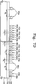
Die zweite Hartmaskenschicht 64 kann dann einem Rückätz-Arbeitsschritt unterzogen werden zum Entfernen von Abschnitten der Hartmaskenschicht 64 zwischen benachbarten Masseauswahlleitungs-Hartmaskenmustern 60g, zwischen benachbarten Reihenauswahlleitungs-Hartmaskenmustern 60s und von oberen Oberflächen der Opfermaskenschicht 62, wie in 5C gezeigt ist. Nach dem Rückätz-Arbeitsschritt verbleibende Abschnitte der zweiten Hartmaskenschicht 64 können somit etwa die Dicke F1 besitzen. Genauer können nach dem Rückätz-Arbeitsschritt verbleibende Abschnitte der zweiten Hartmaskenschicht 64 ein zweites Hartmaskenmuster 70 auf der Opfermaskenschicht 62 definieren. Das zweite Hartmaskenmuster 70 kann ein Dummy-Wortleitungsmuster 70d zwischen dem Masseauswahlleitungsmuster 60g und dem ersten ungeraden Wortleitungsmuster 60w sowie gerade Wortleitungsmuster 70w zwischen benachbarten ungeraden Wortleitungsmustern 60w sowie zwischen dem letzten ungeraden Wortleitungsmuster 60w und dem Reihenauswahlleitungsmuster 60s enthalten.The second hard mask layer 64 may then be subjected to an etch-back operation to remove portions of the hardmask layer 64 between adjacent ground select line hard mask patterns 60g , between adjacent row select line hardmask patterns 60s and upper surfaces of the sacrificial mask layer 62 , as in 5C is shown. After the etch-back operation, remaining portions of the second hard mask layer remain 64 can thus have about the thickness F 1 . More specifically, after the etch back process, remaining portions of the second hard mask layer may be left 64 a second hard mask pattern 70 on the sacrificial mask layer 62 define. The second hard mask pattern 70 can be a dummy word line pattern 70d between the ground selection line pattern 60g and the first odd word line pattern 60w as well as straight word line pattern 70w between adjacent odd word line patterns 60w and between the last odd word line pattern 60w and the row selection line pattern 60s contain.
Freiliegende Abschnitte der Opfermaskenschicht 62 können dann entfernt werden (z. B. durch Trockenätzen), wie in 5D gezeigt ist, zum Freilegen von Abschnitten der Ätzzielschicht 52, die nicht von den ersten und/oder zweiten Hartmaskenmustern 60 und/oder 70 bedeckt sind. Freiliegende Abschnitte der Ätzzielschicht 52 können dann entfernt werden (z. B. durch Trockenätzen), wobei die ersten und zweiten Hartmaskenmuster 60 und 70 als eine Ätzmaske verwendet werden, und die ersten und zweiten Hartmaskenmuster 60 und 70 können dann entfernt werden zum Bereitstellen der Struktur aus den 2A–B.Exposed sections of the sacrificial mask layer 62 can then be removed (eg by dry etching) as in 5D is shown for exposing portions of the etching target layer 52 not from the first and / or second hardmask patterns 60 and or 70 are covered. exposed Portions of the etch target layer 52 can then be removed (eg, by dry etching) using the first and second hardmask patterns 60 and 70 are used as an etching mask, and the first and second hardmask patterns 60 and 70 can then be removed to provide the structure from the 2A -B.
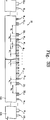
3A ist eine Draufsicht einer nichtflüchtigen Speichervorrichtung 30 (wie z. B. einer Flash-Speichervorrichtung) gemäß einigen Ausführungsformen der vorliegenden Erfindung, und 3B ist eine Querschnittsansicht entlang der Schnittlinie II-II' aus 3A. Die Flash-Speichervorrichtung 30 kann eine Mehrzahl von parallelen aktiven Bereichen ACT in einem Halbleitersubstrat SUB, getrennt durch Vorrichtungsisolierschichten enthalten. Zusätzlich können Masseauswahlleitungen GSL0-2, Reihenauswahlleitungen SSL0-2, Dummy-Wortleitungen WLd und Speicherzellen-Wortleitungen WL1-2n (wobei n eine ganze Zahl ist) die aktiven Bereiche ACT kreuzen. Genauer kann ein jeweiliges Ladungsspeichergate zwischen jeder Speicherzellen-Wortleitung WL1-2n und jedem aktiven Bereich ACT vorgesehen sein zum Bereitstellen einer jeweiligen Speicherzelle an jeder Überschneidung einer Speicherzellen-Wortleitung WL1-2n mit einem aktiven Bereich ACT. Genauso kann ein Ladungsspeichergate zwischen jeder Dummy-Wortleitung WLd und dem aktiven Bereich ACT vorgesehen sein, so dass die Strukturen der Dummy-Wortleitungen WLd und der Speicherzellen-Wortleitungen WL1-2n die gleichen sind. 3A Fig. 10 is a plan view of a nonvolatile memory device 30 (such as a flash memory device) according to some embodiments of the present invention, and 3B is a cross-sectional view along the section line II-II 'from 3A , The flash memory device 30 may include a plurality of parallel active regions ACT in a semiconductor substrate SUB separated by device isolation layers. In addition, ground select lines GSL 0-2 , row select lines SSL 0-2 , dummy word lines WL d, and memory cell word lines WL 1-2n (where n is an integer) may cross the active areas ACT. More specifically, a respective charge storage gate may be provided between each memory cell word line WL 1-2n and each active area ACT for providing a respective memory cell at each intersection of a memory cell word line WL 1-2n with an active area ACT. Similarly, a charge storage gate may be provided between each dummy word line WL d and the active area ACT, so that the structures of the dummy word lines WL d and the memory cell word lines WL 1-2n are the same.
Eine gerade Anzahl an Speicherzellen-Wortleitungen WL1-2n entlang einem aktiven Bereich ACT zwischen einer Masseauswahlleitung GSL und einer Reihenauswahlleitung SSL (z. B. zwischen GSL1 und SSL1) können eine Speicherzellen-Reihe mit einer geraden Anzahl an Speicherzellen definieren. Wie weiter in den 3A–B gezeigt ist können benachbarte Speicherzellenreihen durch zwei Masseauswahlleitungen GSL (z. B. GSL0 und GSL1) oder durch zwei Reihenauswahlleitungen SSL (z. B. SSL1 und SSL2) voneinander getrennt sein. Genauer können 2k (wobei k eine positive ganze Zahl ist) Speicherzellen-Wortleitungen WL1-2n eine Speicherzellen-Reihe mit 2k zum Speichern von Daten verwendeten Speicherzellen definieren. Die Dummy-Wortleitung WLd wird jedoch nicht zum Speichern von Daten verwendet.An even number of memory cell word lines WL 1-2n along an active area ACT between a ground select line GSL and a row select line SSL (eg, between GSL 1 and SSL 1 ) may define a memory cell array having an even number of memory cells. As further in the 3A -B adjacent memory cell rows may be separated by two ground select lines GSL (eg GSL 0 and GSL 1 ) or by two row select lines SSL (eg SSL 1 and SSL 2 ). More specifically can 2 k (where k is a positive integer) memory cell word lines WL 1-2n define a memory cell row with 2 k used for storing data memory cells. However, the dummy word line WL d is not used for storing data.
Darüber hinaus kann eine Anordnung von Speicherzellen-Wortleitungen WL1-2n und einer Dummy-Wortleitung WLd von benachbarten Speicherzellen-Reihen eine Spiegelsymmetrie besitzen. Z. B. kann eine Anordnung von Speicherzellen-Wortleitungen WL1-2n und einer Dummy-Wortleitung WLd zwischen der Masseauswahlleitung GLS0 und der Reihenauswahlleitung SSL0 Spiegelsymmetrie relativ zu einer Anordnung von Speicherzellen-Wortleitungen WL1-2n und einer Dummy-Wortleitung WLd zwischen der Masseauswahlleitung GSL1 und der Reihenauswahlleitung SSL1 besitzen. Genauso kann eine Anordnung von Speicherzellen-Wortleitungen WL1-2n und einer Dummy-Wortleitung WLd zwischen der Masseauswahlleitung GSL1 und der Reihenauswahlleitung SSL1 Spiegelsymmetrie relativ zu einer Anordnung von Speicherzellen-Wortleitungen WL1-2n und einer Dummy-Wortleitung WLd zwischen der Masseauswahlleitung GLS2 und der Reihenauswahlleitung SSL2 besitzen.In addition, an array of memory cell word lines WL 1-2n and a dummy word line WL d of adjacent memory cell rows may have mirror symmetry. For example, an arrangement of memory cell word lines WL 1-2n and a dummy word line WL d between ground select line GLS 0 and row select line SSL 0 may mirror symmetry relative to an array of memory cell word lines WL 1-2n and a dummy word line WL d the ground selection line GSL 1 and the row selection line SSL 1 have. Similarly, an arrangement of memory cell word lines WL 1-2n and a dummy word line WL d between ground select line GSL 1 and row select line SSL 1 may mirror symmetry relative to an array of memory cell word lines WL 1-2n and a dummy word line WL d the ground selection line GLS 2 and the row selection line SSL 2 have.
Durch Bereitstellen einer Dummy-Wortleitung WLd zwischen einer Masseauswahlleitung GSL und einer ersten Speicherzellen-Wortleitung WL1 einer Speicherzellenreihe kann ein masseinduzierter Leckstrom und/oder eine Löschstörung an der ersten Speicherzellen-Wortleitung WL1 verringert werden. Darüber hinaus kann ein Controller der nichtflüchtigen Speichervorrichtung an die Masseauswahlleitungen, die Reihenauswahlleitungen, die Speicherzellen-Wortleitungen und die Dummy-Wortleitungen angeschlossen sein. Während eines Löschvorgangs kann der Controller z. B. derart konfiguriert sein, dass er der Masseauswahlleitung GSL1 ermöglicht, zu schweben, dass eine Löschspannung Vers von etwa 20 V an eine p-Wanne des Substrats SUB angelegt wird, und dass 0 V an die Speicherzellen-Wortleitungen WL1-2n angelegt werden. Zusätzlich kann der Controller derart konfiguriert sein, dass eine Vorspannung Vb an die Dummy-Wortleitung WLd angelegt wird, wobei die Vorspannung Vb zwischen einer Versorgungsspannung Vcc und einer Durchgangsspannung Vpass (d. h. Vcc < Vb < Vpass) ist, um dadurch eine Löschstörung an der ersten Speicherzellenwortleitung WL1 und/oder an jeweiligen Ladungsspeicherschichten zu verringern.By providing a dummy word line WL d between a ground select line GSL and a first memory cell word line WL 1 of a memory cell row, a ground-induced leakage current and / or an erase fault on the first memory cell word line WL 1 can be reduced. In addition, a controller of the nonvolatile memory device may be connected to the ground select lines, the row select lines, the memory cell word lines, and the dummy word lines. During an erase operation, the controller z. B. may be configured to allow the ground selection line GSL 1 to float an erase voltage Ver of about 20V to a p-well of the substrate SUB and to apply 0V to the memory cell word lines WL 1-2n become. In addition, the controller may be configured such that a bias voltage Vb is applied to the dummy word line WL d , where the bias voltage Vb is between a supply voltage Vcc and a continuity voltage Vpass (ie, Vcc <Vb <Vpass), thereby canceling the erase first memory cell word line WL 1 and / or at respective charge storage layers.
Während eines Schreib-(oder Programmier-)Vorgangs kann der Controller derart konfiguriert sein, dass die Versorgungsspannung Vcc an die Masseauswahlleitung GSL1 anlegt wird, dass 0 V an eine p-Wanne des Substrats SUB anlegt wird, dass er eine Durchgangsspannung Vpass an die nicht-ausgewählten Wortleitungen anlegt wird, und dass er eine Programmierspannung Vpgm an die ausgewählte Wortleitung anlegt wird. Zusätzlich kann der Controller derart konfiguriert sein, dass er eine Vorspannung Vb an die Dummy-Wortleitung WLd anlegt, wobei die Vorspannung Vb zwischen der Versorgungsspannung Vcc und der Durchgangsspannung Vpass ist (d. h. Vcc < Vb < Vpass), um dadurch den masseinduzierten Leckstrom an der Masseauswahlleitung benachbart zu der Dummy-Wortleitung zu verringern.During a write (or program) operation, the controller may be configured to apply the supply voltage Vcc to the ground select line GSL 1, apply 0 V to a p-well of the substrate SUB to apply a pass voltage Vpass to the unselected word lines is applied, and that it applies a programming voltage Vpgm to the selected word line. In addition, the controller may be configured to apply a bias voltage Vb to the dummy word line WL d , where the bias voltage Vb is between the supply voltage Vcc and the through voltage Vpass (ie, Vcc <Vb <Vpass), thereby indicating the ground-induced leakage current of the ground select line adjacent to the dummy word line.
Wie in den 3A–B gezeigt können die Dummy-Wortleitungen WLd und jede der Speicherzellen-Wortleitungen WL1 bis WL2n etwa eine gleiche Breite F1 haben. Zusätzlich kann etwa eine gleiche Weite/ein gleicher Abstand W, eine Dummy-Wortleitung WLd und eine benachbarte erste Speicherzellen-Wortleitung WL1 trennen, und kann etwa die gleiche Weite/der gleiche Abstand W1 benachbarte Speicherzellen/Wortleitungen WLx und WLx+1 trennen. Darüber hinaus können die Weiten F1 und W1 etwa gleich sein und insbesondere können jede der Weiten F1 und W1 etwa ein Viertel (1/4) einer Periode P1 sein, die durch benachbarte gerade Speicherzellen-Wortleitungen WLgerade und WLgerade+2 (d. h. die geraden Speicherzellen/Wortleitungen, die nur durch eine ungerade Speicherzellen-Wortleitung getrennt sind) definiert ist oder die durch benachbarte ungerade Speicherzellen-Wortleitungen WLungerade WLungerade+2 (d. h. die ungeraden Speicherzellen-Wortleitungen, die nur durch eine gerade Speicherzellen-Wortleitung getrennt sind) definiert ist.As in the 3A 3B, the dummy word lines WL d and each of the memory cell word lines WL 1 to WL 2n may be approximately equal in width F 1 . In addition, about an equal width / distance W, a dummy word line WL d and an adjacent first one may be used Memory cell word line WL 1 separate, and can about the same width / the same distance W 1 adjacent memory cells / word lines WL x and WL x + 1 separate. Moreover, the widths F 1 and W 1 may be approximately equal, and in particular, each of the widths F 1 and W 1 may be about one quarter (1/4) of a period P 1 caused by adjacent even memory cell word lines WL even and WL even +2 (ie, the even memory cells / wordlines that are only separated by an odd memory cell wordline) or odd + 2 by adjacent odd memory cell wordlines WLungerade WL (ie, the odd memory cell wordlines that are driven only by even memory cells Word line are separated) is defined.
Wie weiter in den 3A–B gezeigt ist, können benachbarte Masseauswahlleitungen GSL0 und SL1 durch etwa eine Weite/einen Abstand W2 getrennt sein, und können benachbarte Reihenauswahlleitungen SSL0 und SSL1 durch die gleiche Weite/den gleichen Abstand W2 getrennt sein. Darüber hinaus kann die zweite Weite/der zweite Abstand W2 zumindest etwa dreimal größer als der Abstand W1 sein. Z. B. kann der zweite Abstand W2 zwischen etwa drei- und viermal größer als der erste Abstand W1 sein, und kann genauer der zweite Abstand W2 mehr als dreimal größer als der erste Abstand W1 und noch genauer mehr als viermal größer als der erste Abstand W1 sein. Außerdem kann eine Weite/ein Abstand W3 eine Gate-Auswahl-Leitung GSL und eine benachbarte Dummy-Wortleitung WLd trennen, und kann etwa die gleiche Weite/der gleiche Abstand W3 eine letzte Speicherzellen-Wortleitung WL2n und eine benachbarte Reihenauswahlleitung SSL trennen. Die Weite/der Abstand W3 kann größer als die Weite/der Abstand W1 und geringer als das zweifache von W1 sein (d. h. W1 < W3 < 2 × W1), und noch genauer kann die Weite/der Abstand W3 größer als das 1,5-fache der Weite/des Abstandes W1 und geringer als das zweifache von W1 sein (d. h. 1,5 × W1 < W3 < 2 × W1).As further in the 3A - B, adjacent ground select lines GSL 0 and SL 1 may be separated by approximately one width W 2 , and adjacent row select lines SSL 0 and SSL 1 may be separated by the same width W 2 . In addition, the second width / the second distance W 2 may be at least about three times greater than the distance W 1 . For example, the second distance W 2 may be between about three and four times greater than the first distance W 1 , and more specifically the second distance W 2 may be more than three times greater than the first distance W 1, and more specifically more than four times greater than the first distance W 2 Be distance W 1 . In addition, a width W 3 may separate a gate select line GSL and an adjacent dummy word line WL d , and may have about the same width / spacing W 3 a last memory cell word line WL 2n and an adjacent row select line SSL separate. The width / the distance W 3 can be greater than the width / the distance W 1 and less than two times of W 1 (ie, W 1 <W 3 <2 × W 1), and more specifically, the width / the distance W 3 is greater than 1.5 times the width W 1 and less than twice W 1 (ie, 1.5 x W 1 <W 3 <2 x W 1 ).
Jede Speicherzellen-Wortleitung WL1 bis WL2n kann somit eine jeweilige Steuerelektrode für eine nicht-flüchtige Speicherzelle (z. B. eine Flash-Speicherzelle) einer Speicherzellen-Reihe auf einem gleichen aktiven Bereich ACT zwischen einer Masseauswahlleitung (z. B. GLS1) und einer Reihenauswahlleitung (z. B. SSL1) bereitstellen. Jede nicht-flüchtige Speicherzelle kann außerdem eine Ladungsspeicherschicht zwischen der jeweiligen Speicherzellen-Wortleitung und dem aktiven Bereich, eine Tunnelisolierschicht zwischen dem aktiven Bereich und der Ladungsspeicherschicht, sowie eine Barrierenisolierschicht zwischen der Speicherzellen-Wortleitung und der Ladungsspeicherschicht enthalten.Each memory cell word line WL 1 to WL 2n may thus have a respective non-volatile memory cell (eg, a flash memory cell) control gate of a memory cell array on a same active area ACT between a ground select line (eg, GLS 1 ) and a row select line (eg, SSL 1 ). Each non-volatile memory cell may further include a charge storage layer between the respective memory cell word line and the active region, a tunnel insulating layer between the active region and the charge storage layer, and a barrier insulating layer between the memory cell word line and the charge storage layer.
Jede Dummy-Wortleitung WLd kann eine gleiche Struktur wie oben diskutiert mit Bezug auf die Speicherzellen-Wortleitungen besitzen (mit einer Tunnelisolierschicht, einer Ladungsspeicherschicht und einer Barrierenisolierschicht zwischen jeder Dummy-Wortleitung und jeweiligen aktiven Bereichen). Die Dummy-Zellen-Wortleitungen und die entsprechenden Tunnelisolierschichten, Ladungsspeicherschichten sowie Barriereisolierschichten werden jedoch nicht zum Speichern von Daten, sondern sind stattdessen vorgesehen zum Verringern des masseinduzierten Leckstroms an der benachbarten Masseauswahlleitung während Programmiervorgängen und/oder zum Verringern der Löschvorspannung an der benachbarten Speicherzelle während Löschvorgängen.Each dummy word line WL d may have a similar structure as discussed above with respect to the memory cell word lines (having a tunnel insulating layer, a charge storage layer, and a barrier insulating layer between each dummy word line and respective active regions). However, the dummy cell wordlines and the corresponding tunneling insulating layers, charge storage layers and barrier insulating layers do not store data, but instead are designed to reduce the ground induced leakage current on the adjacent ground select line during programming operations and / or to reduce the erase bias on the adjacent memory cell during erase operations ,
Das Muster von Masseauswahlleitungen GSL, Dummy-Wortleitungen WLd, Speicherzellen-Wortleitungen WL1 bis WL2n sowie Reihenauswahlleitungen SSL kann gebildet werden unter Verwendung von selbstausgerichteter Doppelmusterung wie mehr im Detail unten beschrieben ist. Z. B. können die Masseauswahlleitungen GSL, die Reihennauswahlleitungen SSL, die Dummy-Wortleitungen WLd und die geraden Speicherzellen-Wortleitungen (WL2, WL4, WL6 ... WL2n) entsprechend einem Muster einer Fotolithographiemaske gebildet werden, und können die ungeraden Speicherzellen-Wortleitungen (WL1, WL3, WL5 ... WL2n-1) unter Verwendung der selbstausgerichteten Doppelmusterung gebildet werden.The pattern of ground select lines GSL, dummy word lines WL d , memory cell word lines WL 1 to WL 2n, and row select lines SSL may be formed using self-aligned dual pattern as described in more detail below. For example, the ground select lines GSL, the row select lines SSL, the dummy word lines WL d and the even memory cell word lines (WL 2 , WL 4 , WL 6 ... WL 2n ) may be formed according to a pattern of a photolithography mask, and may be the odd memory cells Word lines (WL 1 , WL 3 , WL 5 ... WL 2n-1 ) are formed using the self-aligned double pattern.
Gemäß einigen Ausführungsformen der vorliegenden Erfindung, die in den 3A–B dargestellt sind, kann eine erste Speicherzellen-Reihe auf einem aktiven Bereich ACT eine erste Mehrzahl von Wortleitungen WL1 bis WL2n enthalten, die den aktiven Bereich ACT zwischen einer ersten Masseauswahlleitung GSL1 und einer ersten Reihenauswahlleitung SSL1 kreuzen, und kann etwa ein gleicher erster Abstand W1 zwischen benachbarten der ersten Mehrzahl von Wortleitungen WL1 bis WL2n vorgesehen sein. Eine zweite Speicherzellen-Reihe auf dem aktiven Bereich ACT kann eine zweite Mehrzahl von Wortleitungen WL1 bis WL2n enthalten, die den aktiven Bereich ACT zwischen einer zweiten Masseauswahlleitung GSL0 und einer zweiten Reihenauswahlleitung SSL0 kreuzen, und etwa der gleiche erste Abstand W1 kann zwischen benachbarten der zweiten Mehrzahl von Wortleitungen WL1 bis WL2n vorgesehen sein. Die erste Masseauswahlleitung GSL1 kann zwischen der zweiten Masseauswahlleitung GSL0 und der ersten Mehrzahl von Wortleitungen sein, und die zweite Masseauswahlleitung GSL0 kann zwischen der ersten Masseauswahlleitung GSL1 und der zweiten Mehrzahl von Wortleitungen sein. Darüber hinaus können Abschnitte des aktiven Bereichs ACT zwischen der ersten und der zweiten Masseauswahlleitung GSL1 und GSL0 frei von Wortleitungen sein, und kann ein zweiter Abstand W2 zwischen der ersten und der zweiten Masseauswahlleitung GSL1 und GSL0 zumindest etwa dreimal größer als der erste Abstand W1 sein. Z. B. kann der zweite Abstand W2 zwischen etwa drei- und viermal größer als der erste Abstand W1 sein, und genauer kann der zweite Abstand W2 mehr als dreimal größer als der erste Abstand W1 und nach genauer mehr als viermal größer als der erste Abstand W1 sein.According to some embodiments of the present invention, which are incorporated in the 3A 1B, a first memory cell row on an active area ACT may include a first plurality of word lines WL 1 to WL 2n crossing the active area ACT between a first ground select line GSL 1 and a first row select line SSL 1 , and may be approximately a same first distance W 1 may be provided between adjacent ones of the first plurality of word lines WL 1 to WL 2n . A second memory cell row on the active area ACT may include a second plurality of word lines WL 1 to WL 2n crossing the active area ACT between a second ground select line GSL 0 and a second row select line SSL 0 , and about the same first distance W 1 may be provided between adjacent ones of the second plurality of word lines WL 1 to WL 2n . The first ground select line GSL 1 may be between the second ground select line GSL 0 and the first plurality of word lines, and the second ground select line GSL 0 may be between the first ground select line GSL 1 and the second plurality of word lines. In addition, sections of the active area ACT between the first and second ground selection lines GSL 1 and GSL 0 are free of word lines, and a second distance W 2 between the first and second ground selection lines GSL 1 and GSL 0 may be at least about three times larger than the first distance W 1 . For example, the second distance W 2 may be between about three and four times greater than the first distance W 1 , and more specifically, the second distance W 2 may be more than three times greater than the first distance W 1 and, more specifically, more than four times greater than the first distance W 2 Be distance W 1 .
Zusätzlich kann die erste Mehrzahl von Wortleitungen WL1 bis WL2n eine gerade Anzahl von Speicherzellen-Wortleitungen enthalten, und kann eine Dummy-Wortleitung WLd zwischen einer ersten der Speicherzellen-Wortleitungen WL1 bis WL2n und der Masseauswahlleitung GSL1 vorgesehen sein. Etwa der gleiche erste Abstand W1 kann zwischen der Dummy-Wortleitung WLd und der ersten der Speicherzellen-Wortleitungen WL1 bis WL2n vorgesehen sein. Darüber hinaus kann ein dritter Abstand W3 zwischen der Masseauswahlleitung GSL1 und der Dummy-Wortleitung WLd vorgesehen sein, und kann der dritte Abstand W3 größer als der erste Abstand W1 und nicht größer als das Zweifache des ersten Abstandes W1 sein (d. h. W1 < W3 < 2 × W1).In addition, the first plurality of word lines WL 1 to WL 2n may include an even number of memory cell word lines, and a dummy word line WL d may be provided between a first one of the memory cell word lines WL 1 to WL 2n and the ground select line GSL 1 . About the same first distance W 1 may be provided between the dummy word line WL d and the first one of the memory cell word lines WL 1 to WL 2n . In addition, a third distance W 3 may be provided between the ground selection line GSL 1 and the dummy word line WL d , and the third distance W 3 may be greater than the first distance W 1 and not greater than twice the first distance W 1 ( ie W 1 <W 3 <2 × W 1 ).
Die 6A–D sind Querschnittsansichten, die Arbeitsschritte des Bildens von nichtflüchtigen Speicherstrukturen aus den 3A–B unter Verwendung von selbstausgerichteter Doppelmusterung gemäß einigen Ausführungsformen der vorliegenden Erfindung darstellen. Wie in 6A gezeigt kann ein Substrat 150 eine Ätzzielschicht 152 darauf enthalten, und kann die Ätzzielschicht 152 Schichten aus Materialien enthalten, die zum Bilden der Speicherzellen, Wortleitungen, Auswahltransistoren und Auswahlleitungen aus 3A–B verwendet werden.The 6A D are cross-sectional views illustrating the operations of forming nonvolatile memory structures from the 3A B using self-aligned dual pattern according to some embodiments of the present invention. As in 6A a substrate can be shown 150 an etching target layer 152 contained on it, and can the etching target layer 152 Layers of materials included for forming the memory cells, word lines, select transistors, and select lines 3A -B be used.
Genauer kann die Ätzzielschicht 152 eine Tunnelisolierschicht (wie z. B. eine Schicht aus Siliziumoxid), eine Ladungsspeichergateschicht (wie z. B. eine Schicht aus Polysilizium oder Siliziumnitrid), eine Barrierenisolierschicht (wie z. B. eine Schicht aus Siliziumoxid oder einem anderen von der Ladungsspeichergateschicht verschiedenen di-elektrischen Material), sowie eine leitfähige Schicht (wie z. B. eine Schicht aus Polysilizium und/oder Metall) enthalten. Die Ladungsspeicherschicht kann zwischen der leitfähigen Schicht und dem Substrat sein, wobei die Tunnelisolierschicht die Ladungsspeicherschicht und das Substrat trennt, und wobei die Barrierenisolierschicht die Ladungsspeicherschicht und die leitfähige Schicht trennt. Zusätzlich kann eine erste Hartmaskenschicht 155 auf der Ätzzielschicht 152 gebildet werden, und kann die erste Hartmaskenschicht 155 eine Siliziumnitridschicht 156 auf einer Pad-Oxidschicht 154 enthalten.More specifically, the etching target layer 152 a tunnel insulating layer (such as a layer of silicon oxide), a charge storage gate layer (such as a layer of polysilicon or silicon nitride), a barrier insulating layer (such as a layer of silicon oxide or another layer different from the charge storage gate layer) -electric material), as well as a conductive layer (such as a layer of polysilicon and / or metal). The charge storage layer may be between the conductive layer and the substrate, wherein the tunnel insulating layer separates the charge storage layer and the substrate, and wherein the barrier insulating layer separates the charge storage layer and the conductive layer. In addition, a first hard mask layer 155 on the etching target layer 152 may be formed, and may be the first hard mask layer 155 a silicon nitride layer 156 on a pad oxide layer 154 contain.
Eine Fotolackschicht auf der ersten Hartmaskenschicht 155 kann unter Verwendung der Fotomaske 200 gemustert werden zum Bereitstellen des Fotolackmusters 158 mit Dummy-Wortleitungs-Fotolackmustern 158d, geraden Wortleitungs-Fotolackmustern 158w, Masseauswahlleitungs-Fotolackmustern 158g und Reihenauswahl-Fotolackmustern 158s. Genauer kann die Fotomaske 200 ein Fotomaskenmuster 204 auf einem transparenten Substrat 202 enthalten. Das Fotomaskenmuster 204 kann Dummy-Wortleitungs-Fotomaskenmuster 204d, die den Dummy-Wortleitungs-Fotolackmustern 158d entsprechen, gerade Wortleitungs-Fotomaskenmuster 204w, die geraden Wortleitungs-Fotolackmustern 158w entsprechen, Masseauswahlleitungs-Fotomaskenmuster 204g, die Masseauswahlleitungs-Fotolackmustern 158g entsprechen sowie Reihenauswahlleitungs-Fotomaskenmuster 204s, die Reihenauswahlleitungs-Fotolackmustern 158s entsprechen, enthalten.A photoresist layer on the first hardmask layer 155 can using the photomask 200 patterned to provide the photoresist pattern 158 with dummy word line photoresist patterns 158d , straight word line photoresist patterns 158W , Earth selection line photoresist patterns 158g and row selection photoresist patterns 158s , More precisely, the photomask 200 a photomask pattern 204 on a transparent substrate 202 contain. The photomask pattern 204 may be dummy wordline photomask pattern 204d patterning the dummy word line photoresist patterns 158d correspond to, just word line photomask patterns 204w , the straight word line photoresist patterns 158W Corresponds to ground selection photo-mask pattern 204g , the earth selection line photoresist patterns 158g correspond as well as row select line photomask patterns 204s , the row selection line photoresist patterns 158s correspond, included.
Wie weiter in 6A gezeigt, können benachbarte gerade Wortleitungs-Fotomaskenmuster 204w durch eine Weite/einen Abstand W11 beabstandet sein, und können benachbarte gerade Wortleitungs-Fotolackmuster 158w durch etwa die Weite/den Abstand W11 beabstandet sein. Ein erstes der geraden Wortleitungs-Fotomaskenmuster 204w kann von einem benachbarten Dummy-Wortleitungs-Fotomaskenmuster 204d durch etwa die Weite/den Abstand W11 beabstandet sein, und ein erstes der geraden Wortleitungs-Fotolackmuster 158w kann von einem benachbarten Dummy-Wortleitungs-Fotolackmuster 158d um etwa die Weite/den Abstand W11 beabstandet sein. Ein Dummy-Wortleitungs-Fotomaskenmuster 204d kann von einem benachbarten Masseauswahlleitungs-Fotomaskenmuster 204d durch einen Abstand W3 beabstandet sein, und ein letztes der geraden Wortleitungs-Fotolackmuster 204w kann von einem benachbarten Reihenauswahlleitungs-Fotomaskenmuster 204s durch etwa die Weite/den Abstand W3 beabstandet sein. Genauso kann ein Dummy-Wortleitungs-Fotolackmuster 158d von einem benachbarten Masseauswahlleitungs-Fotolackmuster 158g durch etwa die Weite/den Abstand W3 beabstandet sein, und kann ein letztes der geraden Wortleitungs-Fotomaskenmuster 158w von einem benachbarten Reihenauswahlleitungs-Fotomaskenmuster 158s durch etwa die Weite/den Abstand W3 beabstandet sein.As in further 6A may show adjacent even wordline photomask patterns 204w may be spaced apart by a width W 11 , and may include adjacent even word line photoresist patterns 158W be spaced by about the width / distance W 11 . A first one of the even wordline photomask patterns 204w may be from an adjacent dummy wordline photomask pattern 204d be spaced apart by about the width W 11 and a first one of the even word line photoresist patterns 158W may be from an adjacent dummy wordline photoresist pattern 158d be spaced by about the width / distance W 11 . A dummy word line photomask pattern 204d may be from an adjacent ground select line photomask pattern 204d by a distance W 3 , and a last one of the even word line photoresist patterns 204w may be from an adjacent row select line photomask pattern 204s be spaced by about the width / the distance W 3 . Likewise, a dummy wordline photoresist pattern may be used 158d from an adjacent ground select line photoresist pattern 158g 3 be spaced by about the width / the distance W, and may be a last word line of the straight photomask pattern 158W from an adjacent row select line photomask pattern 158s be spaced by about the width / the distance W 3 .
Darüber hinaus kann jedes der geraden Wortleitungs-Fotomaskenmuster 204w und jedes der geraden Wortleitungs-Fotolackmuster 158w eine Breite von etwa F1 besitzen, und kann die Weite/der Abstand W3 in den Bereich von zumindest etwa der Breite F1 bis nicht größer als etwa das Zweifache der Breite F1(F1 ≤ W3 ≤ 2 × F1) sein. Zusätzlich können benachbarte der geraden Wortleitungs-Fotomaskenmuster 204w und benachbarte der geraden Wortleitungs-Fotolackmuster 158w eine Periode P1 definieren, und kann die Periode P1 etwa das Vierfache der Breite F1 sein. Die Breite F1 kann eine minimale Strukturgröße sein, die für die verwendete Fotolithographietechnik verfügbar ist. Benachbarte Masseauswahlleitungs-Fotomaskenmuster 204g, benachbarte Reihenauswahlleitungs-Fotomaskenmuster 204s, benachbarte Masseauswahlleitungs-Fotolackmuster 158g und benachbarte Reihenauswahlleitungs-Fotolackmuster 158s können durch eine Weite/einen Abstand W2 getrennt sein, und die Weite/der Abstand W2 können größer als dass Dreifache der Breite F1 sein. Z. B. kann der zweite Abstand W2 zwischen etwa drei- und viermal größer als der erste Abstand W1 sein, oder kann der zweite Abstand W2 mehr als dreimal größer als der erste Abstand W1, und noch genauer mehr als viermal größer als der erste Abstand W1 sein.In addition, each of the even word line photomask patterns 204w and each of the even wordline photoresist patterns 158W have a width of about F 1 , and the width / distance W 3 may be in the range of at least about the width F 1 to not greater than about twice the width F 1 (F 1 ≦ W 3 ≦ 2 × F 1 ) be. In addition, adjacent ones of the even word line photomask patterns may be used 204w and adjacent to the even word line photoresist patterns 158W define a period P 1 , and the period P 1 may be about four times the width F 1 . The width F 1 may be a minimum feature size available for the photolithography technique used. Neighboring ground selection line photomask patterns 204g adjacent row select line photomask patterns 204s , neighboring ground selection line photoresist patterns 158g and adjacent row select line photoresist patterns 158s may be separated by a width W 2 , and the width W 2 may be greater than three times the width F 1 . For example, the second distance W 2 may be between about three and four times greater than the first distance W 1 , or the second distance W 2 may be more than three times greater than the first distance W 1 , and more particularly more than four times greater than the first distance W 2 Be distance W 1 .
Genauer kann eine durchgehende Fotolackschicht durch die Fotomaske 200 selektiv belichtet und dann entwickelt werden zum Bereitstellen des Fotolackmusters 158 aus 6A. Dementsprechend wird eine Anordnung des Fotolackmusters 158 durch eine Anordnung des Fotomaskenmusters 204 definiert. Zusätzlich entspricht das Fotolackmuster 158 einem Muster von Gate-Auswahlleitungen, Reihenauswahlleitungen und geraden Wortleitungen, die oben mit Bezug auf die 3A–B diskutiert wurden.More specifically, a continuous photoresist layer may pass through the photomask 200 selectively exposed and then developed to provide the photoresist pattern 158 out 6A , Accordingly, an arrangement of the resist pattern becomes 158 by an arrangement of the photomask pattern 204 Are defined. In addition, the photoresist pattern corresponds 158 a pattern of gate select lines, row select lines, and even word lines described above with reference to FIGS 3A -B were discussed.
Abschnitte der ersten Hartmaskenschicht 155 (mit der Siliziumnitridschicht 156 und der Pad-Oxidschicht 154), die durch das Fotolackmuster 158 freigelegt sind, können selektiv entfernt werden (z. B. durch Trockenätzern), um ein erstes Hartmaskenmuster 160 (mit Masseauswahlleitungs-Hartmaskenmustern 160g, Reihenauswahlleitungs-Hartmaskenmustern 160s, Dummy-Wortleitungs-Hartmaskenmustern 160d und geraden Wortleitungs-Hartmaskenmustern 160w) wie in 6B gezeigt bereitzustellen. Wenn die erste Hartmaskenschicht 155 separate Schichten 154 und 156 enthält, kann außerdem jedes Element des ersten Hartmaskenmusters 160 separate Schichten 154 und 156 enthalten. Etwa ein gleicher Abstand/eine gleiche Weite W11 kann vorgesehen sein zwischen einem Dummy-Wortleitungs-Hartmaskenmuster 160d und einem ersten geraden Wortleitungs-Hartmaskenmuster 160w, sowie zwischen benachbarten geraden Wortleitungs-Hartmaskenmustern 160w. Etwa der gleiche Abstand/die gleiche Weite W3 kann vorgesehen sein zwischen einem Masseauswahlleitungs-Hartmaskenmuster 160g und einem Dummy-Wortleitungs-Hartmaskenmuster 160d sowie zwischen einem letzten geraden Wortleitungs-Hartmaskenmuster 160w und einem Reihenauswahlleitungs-Hartmaskenmuster 160s. Jedes Element des ersten Hartmaskenmusters 160 kann eine Schicht aus Siliziumnitrid und/oder Siliziumoxid enthalten. Nach dem selektiven Entfernen von Abschnitten der ersten Hartmaskenschicht kann das Fotolackmuster 158 entfernt werden.Sections of the first hard mask layer 155 (with the silicon nitride layer 156 and the pad oxide layer 154 ) passing through the photoresist pattern 158 can be selectively removed (eg, by dry etch) to form a first hard mask pattern 160 (with ground selection hardmask patterns 160g , Row selection line hard mask patterns 160s , Dummy wordline hardmask patterns 160d and even wordline hardmask patterns 160w ) as in 6B to provide shown. When the first hard mask layer 155 separate layers 154 and 156 Also, any element of the first hardmask pattern may contain 160 separate layers 154 and 156 contain. Approximately an equal distance / an equal width W 11 may be provided between a dummy word line hard mask pattern 160d and a first straight wordline hardmask pattern 160w , as well as between adjacent even wordline hardmask patterns 160w , Approximately the same distance / width W 3 may be provided between a ground select line hard mask pattern 160g and a dummy wordline hardmask pattern 160d and between a last even wordline hardmask pattern 160w and a row select line hard mask pattern 160s , Each element of the first hardmask pattern 160 may contain a layer of silicon nitride and / or silicon oxide. After selectively removing portions of the first hardmask layer, the photoresist pattern may 158 be removed.
Wie weiter in 6B gezeigt, kann eine Opfermaskenschicht 162 auf dem ersten Hartmaskenmuster 160 und auf Abschnitten der Ätzzielschicht 152, die durch das erste Hartmaskenmuster 160 freigelegt sind, gebildet werden, und die Opfermaskenschicht 162 und das erste Hartmaskenmuster 160 können verschiedene Materialien umfassen. Z. B. können obere Schichten 156 des ersten Hartmaskenmusters 160 eine Schicht aus Siliziumnitrid sein, und kann die Opfermaskenschicht 152 eine Schicht aus Polysilizium sein. Darüber hinaus kann eine Dicke der Opfermaskenschicht 162 so bereit gestellt werden, dass: zwischen Abschnitten der Opfermaskenschicht 162 an Seitenwänden von benachbarten der geraden Wortleitungs-Hartmaskenmustern 160w Lücken bleiben; zwischen Abschnitten der Opfermaskenschicht 162 an Seitenwänden von benachbarten Masseauswahlleitungs-Hartmaskenmustern 160g Lücken bleiben; zwischen Abschnitten der Opfermaskenschicht 162 an Seitenwänden von benachbarten Reihenauswahlleitungs-Hartmaskenmustern 160s Lücken bleiben; und zwischen Abschnitten der Opfermaskenschicht 162 an Seitenwänden von benachbarten Dummy-Wortleitungs-Hartmaskenmustern 160d und ersten geraden Wortleitungs-Hartmaskenmustern 160w Lücken bleiben. Jedoch kann die Opfermaskenschicht 162 Lücken zwischen Masseauswahlleitungs-Hartmaskenmustern 160g und Dummy-Wortleitungs-Hartmaskenmustern 160d füllen, und kann die Opferschicht 162 Lücken zwischen einem letzten der geraden Wortleitungs-Hartmaskenmuster 160w und einem benachbarten Reihenauswahlleitungs-Hartmaskenmuster 160s füllen.As in further 6B can show a sacrificial mask layer 162 on the first hardmask pattern 160 and on portions of the etch target layer 152 passing through the first hard mask pattern 160 are exposed, and the sacrificial mask layer 162 and the first hard mask pattern 160 can include different materials. For example, upper layers can 156 of the first hard mask pattern 160 may be a layer of silicon nitride, and may be the sacrificial mask layer 152 be a layer of polysilicon. In addition, a thickness of the sacrificial mask layer 162 be provided so that: between sections of the sacrificial mask layer 162 on sidewalls of adjacent ones of the even wordline hardmask patterns 160w Gaps remain; between sections of the victim mask layer 162 on sidewalls of adjacent ground select line hard mask patterns 160g Gaps remain; between sections of the victim mask layer 162 on sidewalls of adjacent row select line hardmask patterns 160s Gaps remain; and between sections of the victim mask layer 162 on sidewalls of adjacent dummy wordline hardmask patterns 160d and first straight wordline hardmask patterns 160w Gaps remain. However, the sacrificial mask layer 162 Gaps between ground select line hard mask patterns 160g and dummy wordline hardmask patterns 160d fill, and may be the sacrificial layer 162 Gaps between a last one of the even wordline hardmask patterns 160w and an adjacent row select line hard mask pattern 160s to fill.
Eine Dicke der Opfermaskenschicht 162 an Seitenwänden der ersten Hartmaskenmuster 160d, 160w, 160g und 160s kann etwa gleich der Weite/dem Abstand W1 zwischen benachbarten Wortleitungen WLx und WLx+1 sein, die in den 3A–B gezeigt sind. Eine Weite/ein Abstand einer zwischen Abschnitten der Opfermaskenschicht 162 auf benachbarten geraden Wortleitungs-Maskenmustern 160w verbleibenden Lücke kann etwa gleich einer Breite F1 einer ungeraden Wortleitung WL1, WL3, ... WL2n-1 sein, die in den Figuren A–D gezeigt sind.A thickness of the sacrificial mask layer 162 on sidewalls of the first hard mask patterns 160d . 160w . 160g and 160s can be approximately equal to the width / distance W 1 between adjacent word lines WL x and WL x + 1 , which in the 3A -B are shown. A distance / a distance between sections of the sacrificial mask layer 162 on adjacent even wordline mask patterns 160w remaining gap may be approximately equal to a width F 1 of an odd word line WL 1 , WL 3 , ... WL 2n-1 shown in Figs.
Nach den Bildern der Opfermaskenschicht 162 kann eine zweite Hartmaskenschicht 164 auf der Opfermaskenschicht 162 gebildet werden, wie weiter in 6B gezeigt ist. Darüber hinaus kann die zweite Hartmaskenschicht 164 eine Schicht aus Siliziumoxid sein, und kann die zweite Hartmaskenschicht 164 eine Dicke aufweisen, die zumindest die Hälfte der Breite F1 ist, um dadurch Lücken in der Opfermaskenschicht 162 zwischen ungeraden Wortleitungs-Hartmaskenmustern 160w zu füllen. Da breitere Lücken zwischen den benachbarten Masseauswahlleitungs-Hartmaskenmustern 160g und zwischen benachbarten Reihenauswahlleitungs-Hartmaskenmustern 160s vorgesehen sind, können jedoch Lücken 168 in der zweiten Hartmaskenschicht 164 verbleiben. Wenn eine Dicke der zweiten Hartmaskenschicht 164 etwa die Breite F1 einer Wortleitung ist, können benachbarte Masseauswahlleitungsmuster 160g und benachbarte Reihenauswahlleitungsmuster 160s durch eine Weite/einen Abstand von mehr als dem Vierfachen von F1 getrennt sein.After the pictures of the sacrificial mask layer 162 may be a second hardmask layer 164 on the sacrificial mask layer 162 be formed, as further in 6B is shown. In addition, the second hard mask layer 164 may be a layer of silicon oxide, and may be the second hardmask layer 164 have a thickness that is at least half of the width F 1 , thereby leaving gaps in the sacrificial mask layer 162 between odd wordline hardmask patterns 160w to fill. Because wider gaps between the adjacent ground line Hartmaskenmustern 160g and between adjacent row select line hardmask patterns 160s intended but there are gaps 168 in the second hardmask layer 164 remain. When a thickness of the second hard mask layer 164 is about the width F 1 of a word line, adjacent ground select line patterns 160g and adjacent row selection line patterns 160s separated by a distance / distance of more than four times F 1 .
Die zweite Hartmaskenschicht 164 kann dann einem Rückätzen unterzogen werden zum Entfernen von Abschnitten der Hartmaskenschicht 164 zwischen benachbarten Masseauswahlleitungs-Hartmaskenmustern 160g, zwischen benachbarten Reihenauswahlleitungs-Hartmaskenmustern 160s und von oberen Oberflächen der Opfermaskenschicht 162, wie in 6C gezeigt ist. Nach dem Rückätzen verbleibende Abschnitte der zweiten Hartmaskenschicht 164 können daher etwa die Dicke F1 haben. Genauer können Abschnitte der zweiten Hartmaskenschicht 164, die nach dem Rückätzen verbleiben, ein zweites Hartmaskenmuster 170 auf der Opfermaskenschicht 162 definieren. Das zweite Hartmaskenmuster 170 kann ungerade Wortleitungsmuster 170w zwischen benachbarten geraden Wortleitungsmustern 160w sowie zwischen dem letzten ungeraden Wortleitungsmuster 160w und dem Reihenauswahlleitungsmuster 160s enthalten.The second hard mask layer 164 can then be etched back to remove portions of the hardmask layer 164 between adjacent ground select line hard mask patterns 160g , between adjacent row select line hardmask patterns 160s and upper surfaces of the sacrificial mask layer 162 , as in 6C is shown. After etching back remaining portions of the second hard mask layer 164 can therefore have about the thickness F 1 . More specifically, portions of the second hardmask layer 164 remaining after etching back, a second hard mask pattern 170 on the sacrificial mask layer 162 define. The second hard mask pattern 170 may have odd word line patterns 170w between adjacent even wordline patterns 160w and between the last odd word line pattern 160w and the row selection line pattern 160s contain.
Freiliegende Abschnitte der Opfermaskenschicht 162 können dann entfernt werden (z. B. durch Trockenätzen), wie in 6D gezeigt ist, zum Freilegen von Abschnitten der Ätzzielschicht 152, die nicht von dem ersten und/oder dem zweiten Hartmaskenmuster 160 und/oder 170 bedeckt sind. Freiliegende Abschnitte der Ätzzielschicht 152 können dann entfernt werden (z. B. durch Trockenätzen) unter Verwendung des ersten und des zweiten Hartmaskenmusters 160 und 170 als eine Ätzmaske, und die ersten und das zweiten Hartmaskenmuster 160 und 170 können dann entfernt werden, um die Struktur aus den 3A–B bereitzustellen.Exposed sections of the sacrificial mask layer 162 can then be removed (eg by dry etching) as in 6D is shown for exposing portions of the etching target layer 152 not from the first and / or the second hardmask pattern 160 and or 170 are covered. Exposed portions of the etching target layer 152 can then be removed (eg, by dry etching) using the first and second hardmask patterns 160 and 170 as an etch mask, and the first and second hardmask patterns 160 and 170 can then be removed to remove the structure from the 3A -B provide.
4A ist eine Draufsicht einer nicht-flüchtigen Speichervorrichtung 40 (wie z. B. eine Flash-Speichervorrichtung) gemäß einigen Ausführungsformen der vorliegenden Erfindung, und 4B ist eine Querschnittsansicht entlang Schnittlinie IV-IV' aus 4A. Die Flash-Speichervorrichtung 40 kann eine Mehrzahl von parallelen aktiven Bereichen ACT in einem Halbleitersubstrat SUB, getrennt durch Vorrichtungsisolierschichten beinhalten. Zusätzlich können Masseauswahlleitungen GSL0-2, Reihenauswahlleitungen SSL0-2 und Speicherzellen-Wortleitungen WL1-2n (wobei n eine ganze Zahl ist) die aktiven Bereiche ACT kreuzen. Genauer kann ein jeweiliges Ladungsspeichergate zwischen jeder Speicherzellen-Wortleitung WL1-2n und jedem aktiven Bereich ACT vorgesehen sein zum Bereitstellen einer jeweiligen Speicherzelle an jeder Überschneidung einer Speicherzellen-Wortleitung WL1-2n mit einem aktiven Bereich ACT. Die Struktur aus den 4A–B ist gleich der aus den 2A–B, wobei die Dummy-Wortleitungen weggelassen sind. 4A Fig. 10 is a plan view of a non-volatile memory device 40 (such as a flash memory device) according to some embodiments of the present invention, and 4B is a cross-sectional view along section line IV-IV 'from 4A , The flash memory device 40 may include a plurality of parallel active regions ACT in a semiconductor substrate SUB separated by device isolation layers. In addition, ground select lines GSL 0-2 , row select lines SSL 0-2, and memory cell word lines WL 1-2n (where n is an integer) may cross the active areas ACT. More specifically, a respective charge storage gate may be provided between each memory cell word line WL 1-2n and each active area ACT for providing a respective memory cell at each intersection of a memory cell word line WL 1-2n with an active area ACT. The structure of the 4A -B is equal to the one from the 2A -B, with the dummy word lines omitted.
Eine gerade Anzahl an Speicherzellen-Wortleitungen WL1-2n entlang eines aktiven Bereiches ACT zwischen einer Masseauswahlleitung GSL und einer Reihenauswahlleitung SSL (z. B. zwischen GSL1 und SSL1) kann eine Speicherzellen-Reihe mit einer geraden Anzahl von Speicherzellen definieren. Wie weiter in den 4A–B gezeigt, können benachbarte Speicherzellen-Reihen durch zwei Masseauswahlleitungen GSL (z. B. GSL0 und GSL1) oder durch zwei Reihenauswahlleitungen SSL (z. B. SSL1 und SSL2) getrennt sein. Insbesondere können 2k (wobei k eine ganze positive Zahl ist) Speicherzellen-Wortleitungen WL1-2n eine Speicherzellen-Reihe mit 2k zum Speichern von Daten verwendeten Speicherzellen definieren.An even number of memory cell word lines WL 1-2n along an active area ACT between a ground select line GSL and a row select line SSL (eg, between GSL 1 and SSL 1 ) may define a memory cell array having an even number of memory cells. As further in the 4A - B, adjacent memory cell rows may be separated by two ground select lines GSL (eg GSL 0 and GSL 1 ) or by two row select lines SSL (eg SSL 1 and SSL 2 ). In particular, 2 k (where k is a positive integer) memory cell word lines WL 1-2n define a memory cell row with 2 k used for storing data memory cells.
Darüber hinaus kann eine Anordnung von Speicherzellen-Wortleitungen WL1-2n von benachbarten Speicherzellen-Reihen eine Spiegelsymmetrie besitzen. Z. B. kann eine Anordnung von Speicherzellen-Wortleitungen WL1-2n zwischen der Masseauswahlleitung GSL0 und der Reihenauswahlleitung SSL0 Spiegelsymmetrie relativ zu einer Anordnung von Speicherzellen-Wortleitungen WL1-2n zwischen der Masseauswahlleitung GSL1 und der Reihenauswahlleitung SSL1 besitzen. Genauso kann eine Anordnung von Speicherzellen-Wortleitungen WL1-2n zwischen der Masseauswahlleitung GSL1 und der Reihenauswahlleitung SSL1 Spiegelsymmetrie relativ zu einer Anordnung von Speicherzellen-Wortleitungen WL1-2n zwischen der Masseauswahlleitung GSL2 und der Reihenauswahlleitung SSL2 besitzen. Durch Bereitstellen eines ausreichenden Abstandes/einer ausreichenden Weite WL4 zwischen einer Masseauswahlleitung GSL und einer ersten Speicherzellen-Wortleitung WL1 einer Speicherzellen-Reihe kann ein masseinduzierter Leckstrom und/oder eine Löschstörung an der ersten Speicherzellen-Wortleitung WL1 verringert werden.In addition, an array of memory cell word lines WL 1-2n of adjacent memory cell rows may have mirror symmetry. For example, an array of memory cell word lines WL 1-2n between ground select line GSL 0 and row select line SSL 0 may have mirror symmetry relative to an array of memory cell word lines WL 1-2n between ground select line GSL 1 and row select line SSL 1 . Similarly, an array of memory cell word lines WL 1-2n between ground select line GSL 1 and row select line SSL 1 may have mirror symmetry relative to an array of memory cell word lines WL 1-2n between ground select line GSL 2 and row select line SSL 2 . By providing a sufficient distance / width WL 4 between a ground select line GSL and a first memory cell word line WL 1 of a memory cell row, a ground-induced leakage current and / or an erase fault on the first memory cell word line WL 1 can be reduced.
Ein Controller der nicht-flüchtigen Speichervorrichtung kann an die Masseauswahlleitungen, die Reihenauswahlleitungen und die Speicherzellen-Wortleitungen angeschlossen sein. Während eines Löschvorgangs kann der Controller z. B. derart konfiguriert sein, dass er der Masseauswahlleitung GSL1 ermöglicht, zu schweben, dass er eine Löschspannung Vers von etwa 20 Volt an eine p-Wanne des Substrates SUB anlegt und dass er 0 Volt an die Speicherzellen-Wortleitungen WL1-2n anlegt. Während eines Schreib-(oder Programmier-)Vorgangs kann der Controller derart konfiguriert sein, dass er die Versorgungsspannung Vcc an die Masseauswahlleitung GSL1 anlegt, dass er 0 Volt an eine p-Wanne des Substrates SUB anlegt und dass er eine Durchgangsspannung Vpass an die nicht-ausgewählten Wortleitungen anlegt, sowie eine Programmierspannung Vpgm an die ausgewählten Wortleitungen anlegt.A controller of the non-volatile memory device may be connected to the ground select lines, the row select lines, and the memory cell word lines. During an erase operation, the controller z. B. configured to allow the ground select line GSL 1 to float to apply an erase voltage vers of about 20 volts to a p-well of the substrate SUB and to apply 0 volts to the memory cell word lines WL 1-2n , During a write (or program) operation, the controller may be configured to apply the supply voltage Vcc to the ground select line GSL 1 , to apply 0 volts to a p-well of the substrate SUB, and to have a Passing voltage Vpass applied to the non-selected word lines, and applies a programming voltage Vpgm to the selected word lines.
Wie in den 4A–B gezeigt, kann jede der Speicherzellen-Wortleitungen WL1 bis WL2n etwa eine gleiche Breite F1 besitzen, und kann eine Weite/ein Abstand W5 eine Gate-Auswahlleitung GSL und eine benachbarte erste Speicherzellen-Wortleitung WL1 einer zugehörigen Speicherzellen-Reihe trennen. Etwa die gleiche Weite/der gleiche Abstand W1 kann benachbarte Speicherzellen-Wortleitungen WLx und WLx+1 trennen, und etwa die gleiche Weite/der gleiche Abstand W1 kann eine letzte Speicherzellen-Wortleitung WL2n und eine benachbarte Reihenauswahlleitung SSL trennen. Darüber hinaus können die Weiten F1 und W1 etwa gleich sein, und genauer kann jede der Weiten F1 und W1 jeweils etwa ein Viertel (1/4) einer Periode Pi sein, die durch benachbarte gerade Speicherzellen-Wortleitungen WLgerade und WLgerade+2 (d. h. gerade Speicherzellen-Wortleitungen, die durch nur eine ungerade Speicherzellen-Wortleitung getrennt sind) definiert ist, oder die durch benachbarte ungerade Speicherzellen-Wortleitungen WLungerade und WLungerade+2 (d. h. ungerade Speicherzellen-Wortleitungen, die durch nur eine gerade Speicherzellen-Wortleitung getrennt sind) definiert ist. Wie weiter in den 4A–B gezeigt, können benachbarte Masseauswahlleitungen GSL0 und GSL1 durch etwa eine Weite/einen Abstand W2 getrennt sein, und benachbarte Reihenauswahlleitungen SSL0 und SSL1 können durch etwa die gleiche Weite/den gleichen Abstand W2 getrennt sein. Der Abstand/die Weite W2 kann zumindest etwa dreimal größer als der Abstand/die Weite W1 sein. Darüber hinaus kann der Abstand/die Weite W5 größer als etwa das Dreifache des Abstands/der Weite W1 sein (d. h. W5 > 3 × W1). Z. B. können der zweite und/oder der fünfte Abstand W2 und/oder W5 zwischen etwa drei- und viermal größer als der erste Abstand W1 sein, oder können der zweite und/oder der fünfte Abstand W2 und/oder W5 mehr als dreimal größer als der erste Abstand W1, und noch genauer mehr als viermal größer als der erste Abstand W1 sein.As in the 4A -B, each of the memory cell word lines WL 1 to WL 2n may have about a same width F 1 , and a width / a distance W 5 may be a gate select line GSL and an adjacent first memory cell word line WL 1 of an associated memory cell. Separate row. Approximately the same width / spacing W 1 can separate adjacent memory cell word lines WL x and WL x + 1 , and approximately the same width / spacing W 1 can separate a last memory cell word line WL 2n and an adjacent row select line SSL. Moreover, the widths F 1 and W 1 may be approximately equal, and more specifically, each of the widths F 1 and W 1 may each be about one quarter (1/4) of a period P i that is even and adjacent to adjacent even memory cell word lines WL WL straight + 2 (ie even memory cell word lines, which are separated by only an odd memory cell word line) is defined, or the odd through adjacent odd memory cell word lines WL and WL odd + 2 (ie, odd memory cell word lines by only an even memory cell word line are separated). As further in the 4A - B, adjacent ground select lines GSL 0 and GSL 1 may be separated by approximately one width W 2 , and adjacent row select lines SSL 0 and SSL 1 may be separated by approximately the same width / distance W 2 . The distance / width W 2 may be at least about three times greater than the distance / width W 1 . Moreover, the distance / width W 5 may be greater than about three times the distance / width W 1 (ie, W 5 > 3 × W 1 ). For example, the second and / or the fifth distance W 2 and / or W 5 may be between about three and four times greater than the first distance W 1 , or may be the second and / or the fifth distance W 2 and / or W 5 more than three times greater than the first distance W 1 , and more particularly more than four times greater than the first distance W 1 be.
Jede Speicherzellen-Wortleitung WL1 bis WL2n kann somit eine jeweilige Steuerelektrode für eine nicht-flüchtige Speicherzelle (z. B. eine Flash-Speicherzelle) einer Speicherzellen-Reihe auf einem gleichen aktiven Bereich ACT zwischen einer Masseauswahlleitung (z. B. GSL1) und einer Reihenauswahlleitung (z. B. SSL1) bereitstellen. Jede nicht-flüchtige Speicherzelle kann außerdem eine Ladungsspeicherschicht zwischen der jeweiligen Speicherzellen-Wortleitung und dem aktiven Bereich, eine Tunnelisolierschicht zwischen dem aktiven Bereich und der Ladungsspeicherschicht, sowie eine Barrierenisolierschicht zwischen der Speicherzellen-Wortleitung und der Ladungsspeicherschicht enthalten.Each memory cell word line WL 1 to WL 2n may thus have a respective non-volatile memory cell (eg, flash memory cell) control gate of a memory cell row on a same active area ACT between a ground select line (eg, GSL 1 ) and a row select line (eg, SSL 1 ). Each non-volatile memory cell may further include a charge storage layer between the respective memory cell word line and the active region, a tunnel insulating layer between the active region and the charge storage layer, and a barrier insulating layer between the memory cell word line and the charge storage layer.
Das Muster der Masseauswahlleitungen GSL, der Speicherzellen-Wortleitungen WL1 bis WL2n und der Reihenauswahlleitungen SSL kann gebildet werden durch selbst ausgerichtete Doppelmusterungen, wie unten mehr im Detail diskutiert ist. Z. B. können die Masseauswahlleitungen GSL, die Reihenauswahlleitungen SSL und die ungeraden Speicherzellen-Wortleitungen (WL1, WL3, WL5, ... WL2n-1) entsprechend einem Muster einer Fotolithographiemaske gebildet werden, und können gerade Speicherzellen-Wortleitungen WL2, WL4, WL6, ... WL2n unter Verwendung von selbst ausgerichteter Doppelmusterung gebildet werden.The pattern of the ground select lines GSL, the memory cell word lines WL 1 to WL 2n, and the row select lines SSL may be formed by self-aligned double patterns, as discussed in more detail below. For example, the ground select lines GSL, the row select lines SSL and the odd memory cell word lines (WL 1 , WL 3 , WL 5 , ... WL 2n-1 ) may be formed according to a pattern of a photolithography mask, and may be even memory cell word lines WL 2 , WL 4 , WL 6 , ... WL 2n are formed using self-aligned double patterning.
Gemäß einigen Ausführungsformen der vorliegenden Erfindung, die in den 4A–B dargestellt sind, kann eine erste Speicherzellen-Reihe auf dem aktiven Bereich ACT eine erste Mehrzahl von Speicherzellen-Wortleitungen WL1 bis WL2n enthalten, die den aktiven Bereich ACT zwischen der ersten Masseauswahlleitung GSL1 und der ersten Reihenauswahlleitung SSL1 kreuzen, und etwa ein gleicher erster Abstand W1 kann vorgesehen sein zwischen benachbarten der ersten Mehrzahl von Wortleitungen.According to some embodiments of the present invention, which are incorporated in the 4A -B, a first memory cell row on the active area ACT may include a first plurality of memory cell word lines WL 1 to WL 2n crossing the active area ACT between the first ground select line GSL 1 and the first row select line SSL 1 , and approximately a same first distance W 1 can be provided between adjacent ones of the first plurality of word lines.
Zusätzlich kann eine zweite Speicherzellen-Reihe auf dem aktiven Bereich ACT eine zweite Mehrzahl von Wortleitungen WL1 bis WL2n enthalten, die den aktiven Bereich ACT zwischen einer zweiten Masseauswahlleitung GSL0 und einer zweiten Reihenauswahlleitung SSL0 kreuzen, und etwa der gleiche erste Abstand W1 kann zwischen benachbarten der zweiten Mehrzahl von Wortleitungen vorgesehen sein. Insbesondere kann die erste Masseauswahlleitung GSL1 zwischen der zweiten Masseauswahlleitung GSL0 und der ersten Mehrzahl von Wortleitungen sein, und kann die zweite Masseauswahlleitung GSL0 zwischen der ersten Masseauswahlleitung GSL1 und der zweiten Mehrzahl von Wortleitungen sein. Darüber hinaus können Abschnitte des aktiven Bereichs ACT zwischen der ersten und der zweiten Masseauswahlleitung GSL1 und GSL0 frei von Wortleitungen sein, und der zweite Abstand W2 zwischen der ersten und der zweiten Masseauswahlleitung GSL1 und GSL0 kann zumindest etwa dreimal größer als der erste Abstand W1 sein. Z. B. kann der zweite Abstand W2 zwischen etwa drei- und viermal größer als der erste Abstand W1 sein, und genauer kann der zweite Abstand W2 genauer etwa dreimal größer als der erste Abstand W1 sein. Wie weiter in den 4A–B gezeigt, kann die erste Mehrzahl von Wortleitungen WL1 bis WL2n eine gerade Anzahl von Speicherzellen-Wortleitungen enthalten, und kann ein Abstand/eine Weite W5, der/die größer als das Dreifache des ersten Abstands W1 ist, zwischen der Masseauswahlleitung GSL1 und der ersten Speicherzellen-Wortleitung WL1 der jeweiligen Speicherzellen-Reihe sein. Darüber hinaus kann etwa der erste Abstand/die erste Weite W1 zwischen der letzten Speicherzellen-Wortleitung WL2n der jeweiligen Speicherzellen-Reihe und der Reihenauswahlleitung SSL1 vorgesehen sein, und Abschnitte des aktiven Bereichs ACT zwischen der Masseauswahlleitung GSL1 und der ersten Speicherzellen-Wortleitung WL1 können frei von Wortleitungen sein.In addition, a second memory cell row on the active area ACT may include a second plurality of word lines WL 1 to WL 2n crossing the active area ACT between a second ground select line GSL 0 and a second row select line SSL 0 , and about the same first distance W 1 may be provided between adjacent ones of the second plurality of word lines. Specifically, the first ground select line GSL 1 may be between the second ground select line GSL 0 and the first plurality of word lines, and may be the second ground select line GSL 0 between the first ground select line GSL 1 and the second plurality of word lines. Moreover, portions of the active region ACT between the first and second ground selection lines GSL 1 and GSL 0 may be free of word lines, and the second distance W 2 between the first and second ground selection lines GSL 1 and GSL 0 may be at least about three times larger than that be first distance W 1 . For example, the second distance W 2 may be between about three and four times greater than the first distance W 1 , and more specifically, the second distance W 2 may be more precisely about three times greater than the first distance W 1 . As further in the 4A -B, the first plurality of word lines WL 1 to WL 2n may include an even number of memory cell word lines, and a pitch W 5 greater than three times the first distance W 1 may be between the Mass selection line GSL 1 and the first memory cell word line WL 1 of the respective memory cell row. In addition, about the first distance / the first width W 1 between the last memory cell word line WL 2n of the respective Memory cell row and the row selection line SSL 1 be provided, and portions of the active area ACT between the ground selection line GSL 1 and the first memory cell word line WL 1 may be free of word lines.
Die 7A–D sind Querschnittsansichten, die Arbeitsschritte des Bildens von nicht-flüchtigen Speichervorrichtungen aus den 4A–B unter Verwendung von selbst ausgerichteter Doppelmusterung gemäß einigen Ausführungsformen der vorliegenden Erfindung darstellen. Wie in 7A gezeigt, kann ein Substrat 350 eine Ätzzielschicht 352 darauf enthalten, und die Ätzzielschicht 352 kann Schichten aus Materialien zum Bilden von Speicherzellen-Wortleitungen, Auswahltransistoren und Auswahlleitungen aus 4A–B enthalten.The 7A D are cross-sectional views illustrating the operations of forming nonvolatile memory devices from FIGS 4A B using self-aligned double pattern according to some embodiments of the present invention. As in 7A can be a substrate 350 an etching target layer 352 and the etch target layer 352 may include layers of materials for forming memory cell wordlines, select transistors, and select lines 4A -B included.
Genauer kann die Zielschicht eine Tunnelisolierschicht (wie z. B. eine Schicht aus Siliziumoxid), eine Ladungsspeichergateschicht (wie z. B. eine Schicht aus Polysilizium oder Siliziumnitrid) eine Barrierenisolierschicht (wie z. B. eine Schicht aus Siliziumoxid oder einem anderen von der Ladungsspeichergateschicht verschiedenen dielektrischen Material) sowie eine leitfähige Schicht (wie z. B. eine Schicht aus Polysilizium und/oder Metall) enthalten. Die Ladungsspeicherschicht kann zwischen der leitfähigen Schicht und dem Substrat sein, wobei die Tunnelisolierschicht die Ladungsspeicherschicht und das Substrat trennt, und wobei die Barrierenisolierschicht die Ladungsspeicherschicht und die leitfähige Schicht trennt. Zusätzlich kann eine erste Hartmaskenschicht 355 auf der Ätzzielschicht 352 gebildet werden, und die erste Hartmaskenschicht 355 kann eine Siliziumnitridschicht 356 auf einer Pad-Oxidschicht 354 enthalten.Specifically, the target layer may be a tunnel insulating layer (such as a layer of silicon oxide), a charge storage gate layer (such as a layer of polysilicon or silicon nitride), a barrier insulating layer (such as a layer of silicon oxide or another of the one of FIG Charge storage gate layer of different dielectric material) as well as a conductive layer (such as a layer of polysilicon and / or metal). The charge storage layer may be between the conductive layer and the substrate, wherein the tunnel insulating layer separates the charge storage layer and the substrate, and wherein the barrier insulating layer separates the charge storage layer and the conductive layer. In addition, a first hard mask layer 355 on the etching target layer 352 are formed, and the first hard mask layer 355 may be a silicon nitride layer 356 on a pad oxide layer 354 contain.
Eine Fotolackschicht auf der ersten Hartmaskenschicht 355 kann unter Verwendung der Fotomaske 300 derart gemustert werden, dass das Fotolackmuster 358 mit ungeraden Wortleitungs-Fotolackmustern 358w, Masseauswahlleitungs-Fotolackmustern 358g und Reihenauswahlleitungs-Fotolackmustern 358s bereitgestellt wird. Insbesondere kann die Fotomaske 300 ein Fotomaskenmuster 304 auf einem transparenten Substrat 302 enthalten. Das Fotomaskenmuster 304 kann ungeraden Wortleitungs-Fotolackmustern 358b entsprechende ungerade Wortleitungs-Fotomaskenmuster 304w, Masseauswahlleitungs-Fotolackmustern 358g entsprechende Masseauswahlleitungs-Fotomaskenmuster 304g sowie Reihenauswahlleitungs-Fotolackmustern 304s entsprechende Reihenauswahl-Fotomaskenmuster 158s enthalten.A photoresist layer on the first hardmask layer 355 can using the photomask 300 be patterned such that the photoresist pattern 358 with odd word line photoresist patterns 358w , Earth selection line photoresist patterns 358g and row selection line photoresist patterns 358s provided. In particular, the photomask 300 a photomask pattern 304 on a transparent substrate 302 contain. The photomask pattern 304 can odd wordline photoresist patterns 358b corresponding odd word line photomask patterns 304W , Earth selection line photoresist patterns 358g corresponding ground select line photomask patterns 304g and row select line photoresist patterns 304s corresponding row selection photomask patterns 158s contain.
Wie weiter in 7A gezeigt, können ungerade Wortleitungs-Fotomaskenmuster 304w durch etwa eine Weite/einen Abstand W11 getrennt sein, und können benachbarte ungerade Wortleitungs-Fotolackmuster 358w durch etwa die Weite/den Abstand W11 beabstandet sein. Ein erstes der ungeraden Wortleitungs-Fotomaskenmuster 304w kann von einem benachbarten Masseauswahlleitungs-Fotomaskenmuster 304g durch etwa eine Weite/einen Abstand W5 getrennt sein, und ein letztes der ungeraden Wortleitungs-Fotomaskenmuster 304w kann von einem benachbarten Reihenauswahlleitungs-Fotomaskenmuster 304s durch etwa die Weite/den Abstand W11 beabstandet sein. Genauso kann ein erstes der ungeraden Wortleitungs-Fotolackmuster 358w von einem benachbarten Masseauswahlleitungs-Fotolackmuster 358g durch etwa die Weite/den Abstand W5 beabstandet sein, und kann ein letztes der ungeraden Wortleitungs-Fotomaskenmuster 358w von einem benachbarten Reihenauswahl-Fotomaskenmuster 358s durch etwa die Weite/den Abstand W11 beabstandet sein.As in further 7A can show odd wordline photomask patterns 304W may be separated by about one width W 11 , and may have adjacent odd word line photoresist patterns 358w be spaced by about the width / distance W 11 . A first of the odd wordline photomask patterns 304W may be from an adjacent ground select line photomask pattern 304g be separated by about a width W 5 and a last one of the odd word line photomask patterns 304W may be from an adjacent row select line photomask pattern 304s be spaced by about the width / distance W 11 . Likewise, a first of the odd word line photoresist patterns may be used 358w from an adjacent ground select line photoresist pattern 358g may be spaced by about the width / spacing W 5 , and may be a last one of the odd wordline photomask patterns 358w from an adjacent row selection photomask pattern 358s be spaced by about the width / distance W 11 .
Darüber hinaus kann jedes der ungeraden Wortleitungs-Fotomaskenmuster 304w und jedes der ungeraden Wortleitungs-Fotolackmuster 358w eine Breite von etwa F1 besitzen, und die Weite/der Abstand W11 kann etwa das Dreifache der Breite F1 sein. Zusätzlich können benachbarte der ungeraden Wortleitungs-Fotomaskenmuster 304w und benachbarte der ungeraden Wortleitungs-Fotolackmuster 358w eine Periode P1 definieren, und die Periode P1 kann etwa das Vierfache der Breite F1 sein. Die Breite F1 kann eine minimale Strukturgröße sein, die für die verwendete Lithographietechnik verfügbar ist. Benachbarte Masseauswahlleitungs-Fotomaskenmuster 304g, benachbarte Reihenauswahlleitungs-Fotomaskenmuster 304s, benachbarte Masseauswahlleitungs-Fotolackmuster 358g, sowie benachbarte Reihenauswahlleitungs-Fotolackmuster 358s können durch eine Weite/einen Abstand W2 getrennt sein, und die Weite/der Abstand W2 kann größer als das dreifache der Breite F1 sein. Z. B. kann der zweite Abstand W2 zwischen etwa drei- und viermal größer als der erste Abstand W1 sein, oder der zweite Abstand W2 kann mehr als dreimal größer als der erste Abstand W1, und noch genauer mehr als viermal größer als der erste Abstand W1 sein.In addition, each of the odd word line photomask patterns 304W and each of the odd wordline photoresist patterns 358w have a width of about F 1 , and the width / distance W 11 may be about three times the width F 1 . In addition, adjacent ones of the odd word line photomask patterns may be used 304W and adjacent the odd word line photoresist patterns 358w define a period P 1 , and the period P 1 may be about four times the width F 1 . The width F 1 may be a minimum feature size available for the lithography technique used. Neighboring ground selection line photomask patterns 304g adjacent row select line photomask patterns 304s , neighboring ground selection line photoresist patterns 358g , as well as adjacent row select line photoresist patterns 358s may be separated by a width W 2 , and the width W 2 may be greater than three times the width F 1 . For example, the second distance W 2 may be between about three and four times greater than the first distance W 1 , or the second distance W 2 may be more than three times greater than the first distance W 1 , and more specifically more than four times greater than the first distance W 2 Be distance W 1 .
Zusätzlich kann ein Abstand/eine Weite W5 zwischen einem ersten ungeraden Wortleitungs-Fotomaskenmuster 304w und einem benachbarten Masseauswahlleitungs-Fotomaskenmuster 304g, sowie zwischen einem ersten ungeraden Wortleitungs-Fotolackmuster 358w und einem benachbarten Masseauswahlleitungs-Fotolackmuster 358g größer als W11 sein (z. B. größer als das Dreifache der Breite F1). Z. B. kann der Abstand/die Weite W5 größer als das Vierfache von F1 sein.In addition, a distance W 5 between a first odd word line photomask pattern 304W and an adjacent ground select line photomask pattern 304g , as well as between a first odd wordline photoresist pattern 358w and an adjacent ground select line photoresist pattern 358g greater than W 11 (eg greater than three times the width F 1 ). For example, the distance / width W 5 may be greater than four times F 1 .
Insbesondere kann eine durchgehende Fotolackschicht durch die Fotomaske 300 selektiv Strahlung ausgesetzt und dann entwickelt werden zum Bereitstellen des Fotolackmusters 358 aus 7A. Dementsprechend wird eine Anordnung des Fotolackmusters 358 durch eine Anordnung des Fotomaskenmusters 304 definiert. Zusätzlich entspricht das Fotolackmuster 358 einem Muster von Gateauswahlleitungen, von Reihenauswahlleitungen und von ungeraden Wortleitungen, die oben mit Bezug auf die 4A–B diskutiert wurden.In particular, a continuous photoresist layer can pass through the photomask 300 selectively exposed to radiation and then developed to provide the photoresist pattern 358 out 7A , Accordingly, an arrangement of the resist pattern becomes 358 by an arrangement of the photomask pattern 304 Are defined. In addition, the photoresist pattern corresponds 358 a pattern of gate select lines, row select lines, and odd word lines described above with respect to FIGS 4A -B were discussed.
Abschnitte der ersten Hartmaskenschicht 355 (mit Siliziumnitridschicht 356 und Pad-Oxidschicht 354), die durch das Fotolackmuster 358 freigelegt sind, können selektiv entfernt werden (z. B. durch Trockenätzen) zum Bereitstellen eines Hartmaskenmusters 360 (mit Masseauswahlleitungs-Hartmaskenmustern 360g, Reihenauswahlleitungs-Hartmaskenmustern 360s und ungeraden Wortleitungs-Hartmaskenmustern 360w), wie in 7B gezeigt ist. Wenn die erste Hartmaskenschicht 355 separate Schichten 354 und 356 enthält, kann jedes Element des ersten Hartmaskenmusters 360 außerdem separate Schichten 354 und 356 enthalten. Etwa der gleiche Abstand/die gleiche Weite W5 (größer als W11) kann zwischen einem Masseauswahlleitungs-Hartmaskenmuster 360g und einem ersten ungeraden Wortleitungs-Hartmaskenmuster 360w vorgesehen sein. Etwa der gleiche Abstand/die gleiche Weite W11 kann zwischen benachbarten ungeraden Wortleitungs-Hartmaskenmustern 360w sowie zwischen einem letzten ungeraden Wortleitungs-Hartmaskenmuster 360w, und einem Reihenauswahlleitungs-Hartmaskenmuster 360s vorgesehen sein. Jedes Element des ersten Hartmaskenmuster 360 kann eine Schicht aus Siliziumnitrid und/oder Siliziumoxid enthalten. Nach dem selektiven Entfernen von Abschnitten der ersten Hartmaskenschicht kann das Fotolackmuster 358 entfernt werden.Sections of the first hard mask layer 355 (with silicon nitride layer 356 and pad oxide layer 354 ) passing through the photoresist pattern 358 can be selectively removed (eg, by dry etching) to provide a hard mask pattern 360 (with ground selection hardmask patterns 360g , Row selection line hard mask patterns 360s and odd wordline hardmask patterns 360w ), as in 7B is shown. When the first hard mask layer 355 separate layers 354 and 356 can contain any element of the first hardmask pattern 360 also separate layers 354 and 356 contain. Approximately the same distance / width W 5 (greater than W 11 ) may exist between a ground select line hard mask pattern 360g and a first odd wordline hardmask pattern 360w be provided. Approximately the same distance / width W 11 may exist between adjacent odd wordline hardmask patterns 360w and between a last odd word line hard mask pattern 360w , and a row select line hard mask pattern 360s be provided. Each element of the first hardmask pattern 360 may contain a layer of silicon nitride and / or silicon oxide. After selectively removing portions of the first hardmask layer, the photoresist pattern may 358 be removed.
Wie weiter in 7B gezeigt, kann eine Opfermaskenschicht 362 auf dem ersten Hartmaskenmuster 360 sowie auf Abschnitten der Ätzzielschicht 352 gebildet werden, die durch das erste Hartmaskenmuster 360 freigelegt sind, und die Opfermaskenschicht 362 und das erste Hartmaskenmuster 360 können verschiedene Materialien umfassen.As in further 7B can show a sacrificial mask layer 362 on the first hardmask pattern 360 and on portions of the etch target layer 352 formed by the first hard mask pattern 360 exposed, and the sacrificial mask layer 362 and the first hard mask pattern 360 can include different materials.
Z. B. können obere Schichten 356 des ersten Hartmaskenmusters 360 eine Schicht aus Siliziumnitrid sein, und können die Opfermaskenschichten 362 eine Schicht aus Polysilizium sein. Darüber hinaus kann eine Dicke der Opfermaskenschicht 362 so bereitgestellt werden, dass: Lücken zwischen Abschnitten der Opfermaskenschicht 362 an Seitenwänden von benachbarten der ungeraden Wortleitungs-Hartmaskenmuster 360w bleiben; Lücken zwischen Abschnitten der Opfermaskenschicht 362 an Seitenwänden von benachbarten Masseauswahlleitungs-Hartmaskenmustern 360g bleiben; Lücken zwischen Abschnitten der Opfermaskenschicht 362 an Seitenwänden von benachbarten Reihenauswahlleitungs-Hartmaskenmustern 360s bleiben; Lücken zwischen Abschnitten der Opfermaskenschicht 362 an Seitenwänden von benachbarten Reihenleitungs-Hartmaskenmustern 360g und ersten ungeraden Wortleitungs-Hartmaskenmustern 360w bleiben; und Lücken zwischen Abschnitten der Opfermaskenschicht 362 an Seitenwänden von benachbarten Auswahlleitungs-Hartmaskenmustern 360s und letzten ungeraden Wortleitungs-Hartmaskenmustern 360w bleiben.For example, upper layers can 356 of the first hard mask pattern 360 be a layer of silicon nitride, and can the sacrificial mask layers 362 be a layer of polysilicon. In addition, a thickness of the sacrificial mask layer 362 be provided such that: gaps between portions of the sacrificial mask layer 362 on sidewalls of adjacent ones of the odd word line hardmask patterns 360w stay; Gaps between sections of the victim mask layer 362 on sidewalls of adjacent ground select line hard mask patterns 360g stay; Gaps between sections of the victim mask layer 362 on sidewalls of adjacent row select line hardmask patterns 360s stay; Gaps between sections of the victim mask layer 362 on sidewalls of adjacent row-line hardmask patterns 360g and first odd wordline hardmask patterns 360w stay; and gaps between sections of the victim mask layer 362 on sidewalls of adjacent select line hardmask patterns 360s and last odd word line hard mask patterns 360w stay.
Eine Dicke der Opfermaskenschicht 362 an Seitenwänden der ersten Hartmaskenmuster 360w, 360d und 360s kann etwa gleich der Weite/dem Abstand W1 zwischen benachbarten Wortleitungen WLx und WLx+1 sein, die in den 4A–B gezeigt sind. Eine Weite einer Lücke, die zwischen Abschnitten der Opfermaskenschicht 362 auf benachbarten ungeraden Wortleitungs-Maskenmustern 360w verbleibt, kann etwa gleich einer Breite F1 einer geraden Wortleitung WL2, WL4, WL6, ... WL2n sein, die in den 4A–B gezeigt sind.A thickness of the sacrificial mask layer 362 on sidewalls of the first hard mask patterns 360w . 360d and 360s can be approximately equal to the width / distance W 1 between adjacent word lines WL x and WL x + 1 , which in the 4A -B are shown. A width of a gap between sections of the sacrificial mask layer 362 on adjacent odd wordline mask patterns 360w can remain approximately equal to a width F 1 of a straight word line WL 2 , WL 4 , WL 6 , ... WL 2n be in the 4A -B are shown.
Nach dem Bilden der Opfermaskenschicht 362 kann eine zweite Hartmaskenschicht 364 auf der Opfermaskenschicht 362 gebildet werden, wie weiter in 7B gezeigt ist. Darüber hinaus kann die zweite Hartmaskenschicht 364 eine Schicht aus Siliziumoxid sein, und kann die zweite Hartmaskenschicht 364 eine Dicke besitzen, die zumindest die Hälfte der Breite F1 ist, um dadurch Lücken in der Opfermaskenschicht 362 zwischen ungeraden Wortleitungs-Hartmaskenmustern 360w zu füllen. Da breitere Lücken zwischen benachbarten Masseauswahlleitungs-Hartmaskenmustern 360g, zwischen benachbarten Reihenauswahlleitungs-Hartmaskenmustern 360s, sowie zwischen Masseauswahlleitungs-Hartmaskenmustern 360g und benachbarten ersten ungeraden Wortleitungs-Hartmaskenmustern 360w vorgesehen sind, können jedoch Lücken 368 in der zweiten Hartmaskenschicht 364 verbleiben. Wenn eine Dicke einer zweiten Hartmaskenschicht 364 etwa gleich der Breite F1 einer Wortleitung ist, können benachbarte Masseauswahlleitungs-Muster 360g, benachbarte Auswahlleitungs-Muster 360s, sowie Masseauswahl-Hartmaskenmuster 360g und benachbarte erste ungerade Wortleitungs-Hartmaskenmuster 360w durch eine Weite/einen Abstand größer als das Vierfache von F1 getrennt sein.After forming the sacrificial mask layer 362 may be a second hardmask layer 364 on the sacrificial mask layer 362 be formed, as further in 7B is shown. In addition, the second hard mask layer 364 may be a layer of silicon oxide, and may be the second hardmask layer 364 have a thickness which is at least half of the width F 1 , thereby leaving gaps in the sacrificial mask layer 362 between odd wordline hardmask patterns 360w to fill. Because wider gaps between adjacent ground select line hard mask patterns 360g , between adjacent row select line hardmask patterns 360s , as well as between ground select line hard mask patterns 360g and adjacent first odd word line hardmask patterns 360w However, there are gaps 368 in the second hardmask layer 364 remain. When a thickness of a second hard mask layer 364 is approximately equal to the width F 1 of a wordline, adjacent ground select line patterns 360g , adjacent select line patterns 360s , as well as mass selection hardmask pattern 360g and adjacent first odd wordline hardmask patterns 360w be separated by a distance greater than four times F 1 .
Die zweite Hartmaskenschicht 364 kann dann einem Rückätzvorgang unterzogen werden zum Entfernen von Abschnitten der Hartmaskenschicht 364 zwischen benachbarten Masseauswahlleitungs-Hartmaskenmustern 360g, zwischen benachbarten Reihenauswahlleitungs-Hartmaskenmustern 360s, zwischen Masseauswahl-Hartmaskenmustern 360g und benachbarten ersten ungeraden Wortleitungs-Hartmaskenmustern 360w, sowie von oberen Oberflächen der Opfermaskenschicht 362, wie in 7C gezeigt ist. Abschnitte der zweiten Hartmaskenschicht 364, die nach dem Rückätzvorgang verbleiben, können somit etwa die Dicke F1 besitzen. Genauer können Abschnitte der zweiten Hartmaskenschicht 364, die nach dem Rückätzvorgang verbleiben, ein zweites Hartmaskenmuster 370 auf der Opfermaskenschicht 362 definieren. Das zweite Hartmaskenmuster 370 kann gerade Wortleitungsmuster 370w zwischen benachbarten ungeraden Wortleitungs-Mustern 360w, sowie zwischen den letzten ungeraden Wortleitungs-Mustern 360w und dem benachbarten Reihenauswahlleitungs-Muster 360s enthalten.The second hard mask layer 364 may then be subjected to an etch back process to remove portions of the hardmask layer 364 between adjacent ground select line hard mask patterns 360g , between adjacent row select line hardmask patterns 360s , between mass selection hardmask patterns 360g and adjacent first odd word line hardmask patterns 360w , as well as upper surfaces of the sacrificial mask layer 362 , as in 7C is shown. Sections of the second hard mask layer 364 , which remain after the Rückätzvorgang, thus may have about the thickness F 1 . More specifically, portions of the second hardmask layer 364 remaining after the etch back process, a second hard mask pattern 370 on the sacrificial mask layer 362 define. The second hard mask pattern 370 can just word line pattern 370w between adjacent odd word line patterns 360w , as well as between the last odd word line patterns 360w and the adjacent row selection line pattern 360s contain.
Freigelegte Abschnitte der Opfermaskenschicht 362 können dann entfernt werden (z. B. durch Trockenätzen) wie in 7D gezeigt ist zum Freilegen von Abschnitten der Ätzzielschicht 352, die nicht von der ersten und/oder der zweiten Hartmaskenschicht 360 und/oder 370 bedeckt sind. Freigelegte Abschnitte der Ätzzielschicht 352 können dann entfernt werden (z. B. durch Trockenätzen) unter Verwendung des ersten und des zweiten Hartmaskenmusters 360 und 370 als eine Ätzmaske, und die ersten und zweiten Hartmaskenmuster 360 und 370 können dann entfernt werden zum Bereitstellen der Struktur aus den 4A–B.Exposed sections of the sacrificial mask layer 362 can then be removed (eg by dry etching) as in 7D is shown for exposing portions of the etching target layer 352 not from the first and / or the second hardmask layer 360 and or 370 are covered. Exposed sections of the etching target layer 352 can then be removed (eg, by dry etching) using the first and second hardmask patterns 360 and 370 as an etch mask, and the first and second hardmask patterns 360 and 370 can then be removed to provide the structure from the 4A -B.
Gemäß Ausführungsformen der vorliegenden Erfindung können nicht-flüchtige Speichervorrichtungen vom NAND-Typ mit Strukturen mit Abmessungen vorgesehen sein, die kleiner sind als Abmessungen, die verfügbar sein können beim Verwenden einer von Ätzen gefolgten fotolithographischen Belichtung. Dementsprechend können nicht-flüchtige Speichervorrichtungen vom NAND-Typ mit relativ feinen Linien– und Raum-Mustern (wie z. B. Mustern von Wortleitungen) bereitgestellt werden, und vergrößerte Integrationsdichte und/oder erhöhte Leistungsfähigkeit kann resultieren.According to embodiments of the present invention, non-volatile NAND-type memory devices may be provided with structures having dimensions smaller than dimensions that may be available using a photolithographic exposure followed by etching. Accordingly, NAND type nonvolatile memory devices may be provided with relatively fine line and space patterns (such as patterns of word lines), and increased integration density and / or increased performance may result.