DE102004030552B4 - Layer arrangement, field effect transistor and method for producing a layer arrangement - Google Patents
Layer arrangement, field effect transistor and method for producing a layer arrangement Download PDFInfo
- Publication number
- DE102004030552B4 DE102004030552B4 DE102004030552A DE102004030552A DE102004030552B4 DE 102004030552 B4 DE102004030552 B4 DE 102004030552B4 DE 102004030552 A DE102004030552 A DE 102004030552A DE 102004030552 A DE102004030552 A DE 102004030552A DE 102004030552 B4 DE102004030552 B4 DE 102004030552B4
- Authority
- DE
- Germany
- Prior art keywords
- layer
- carbon
- semiconductor layer
- trench
- silicon
- Prior art date
- Legal status (The legal status is an assumption and is not a legal conclusion. Google has not performed a legal analysis and makes no representation as to the accuracy of the status listed.)
- Expired - Fee Related
Links
Classifications
-
- H—ELECTRICITY
- H10—SEMICONDUCTOR DEVICES; ELECTRIC SOLID-STATE DEVICES NOT OTHERWISE PROVIDED FOR
- H10D—INORGANIC ELECTRIC SEMICONDUCTOR DEVICES
- H10D30/00—Field-effect transistors [FET]
- H10D30/60—Insulated-gate field-effect transistors [IGFET]
- H10D30/67—Thin-film transistors [TFT]
- H10D30/6729—Thin-film transistors [TFT] characterised by the electrodes
- H10D30/6737—Thin-film transistors [TFT] characterised by the electrodes characterised by the electrode materials
- H10D30/6739—Conductor-insulator-semiconductor electrodes
-
- H—ELECTRICITY
- H10—SEMICONDUCTOR DEVICES; ELECTRIC SOLID-STATE DEVICES NOT OTHERWISE PROVIDED FOR
- H10D—INORGANIC ELECTRIC SEMICONDUCTOR DEVICES
- H10D30/00—Field-effect transistors [FET]
- H10D30/60—Insulated-gate field-effect transistors [IGFET]
- H10D30/67—Thin-film transistors [TFT]
- H10D30/674—Thin-film transistors [TFT] characterised by the active materials
-
- H—ELECTRICITY
- H10—SEMICONDUCTOR DEVICES; ELECTRIC SOLID-STATE DEVICES NOT OTHERWISE PROVIDED FOR
- H10D—INORGANIC ELECTRIC SEMICONDUCTOR DEVICES
- H10D30/00—Field-effect transistors [FET]
- H10D30/60—Insulated-gate field-effect transistors [IGFET]
- H10D30/67—Thin-film transistors [TFT]
- H10D30/6757—Thin-film transistors [TFT] characterised by the structure of the channel, e.g. transverse or longitudinal shape or doping profile
-
- H—ELECTRICITY
- H10—SEMICONDUCTOR DEVICES; ELECTRIC SOLID-STATE DEVICES NOT OTHERWISE PROVIDED FOR
- H10D—INORGANIC ELECTRIC SEMICONDUCTOR DEVICES
- H10D64/00—Electrodes of devices having potential barriers
- H10D64/01—Manufacture or treatment
- H10D64/018—Spacers formed inside holes at the prospective gate locations, e.g. holes left by removing dummy gates
-
- H—ELECTRICITY
- H10—SEMICONDUCTOR DEVICES; ELECTRIC SOLID-STATE DEVICES NOT OTHERWISE PROVIDED FOR
- H10D—INORGANIC ELECTRIC SEMICONDUCTOR DEVICES
- H10D64/00—Electrodes of devices having potential barriers
- H10D64/01—Manufacture or treatment
- H10D64/025—Manufacture or treatment forming recessed gates, e.g. by using local oxidation
- H10D64/027—Manufacture or treatment forming recessed gates, e.g. by using local oxidation by etching at gate locations
Landscapes
- Thin Film Transistor (AREA)
Abstract
Schicht-Anordnung,
• mit einem
Substrat (101);
• mit
einer Halbleiter-Schicht (103, 201) auf dem Substrat (101);
• mit einem
Graben (704) in der Halbleiter-Schicht (201);
• mit elektrisch
isolierendem Material (801, 802) an den Seitenwänden und am Boden des Grabens
(704);
• mit
Kohlenstoff aufweisendem elektrisch leitfähigem Material (1101) auf dem
elektrisch isolierenden Material (802) in dem Graben (704).Layer arrangement,
• with a substrate (101);
With a semiconductor layer (103, 201) on the substrate (101);
• with a trench (704) in the semiconductor layer (201);
With electrically insulating material (801, 802) on the sidewalls and bottom of the trench (704);
Carbon conductive electroconductive material (1101) on the electrically insulating material (802) in the trench (704).
Description
Die Erfindung betrifft eine Schicht-Anordnung, einen Feldeffekttransistor und ein Verfahren zum Herstellen einer Schicht-Anordnung.The The invention relates to a layer arrangement, a field effect transistor and a method of making a layer assembly.
Sogenannte fully-depleted Silicon-on-Insulator (FD-SOI) Devices mit ultradünnen Kanal-Bereichen werden als vielversprechende Alternative für konventionelle Bulk-Substrat-Transistoren in künftigen CMOS-Generationen angesehen. Ein fully-depleted Silicon-on-Insulator Device kann die Anforderungen der ITRS ("International Technology Roadmap für Semiconductors") erfüllen. Durch die extreme Skalierung der Kanaldicke (insbesondere im Bereich von 10 nm und weniger) entsprechend der Gate-Länge (z. B. Verhältnis 1:4) kann insbesondere ein geforderter geringer Off-Strom eines FD-SOI-Transistors erreicht werden.So-called Fully-depleted silicon-on-insulator (FD-SOI) devices with ultra-thin channel regions are considered a promising alternative for conventional bulk-substrate transistors in future Viewed in CMOS generations. A fully-depleted silicon-on-insulator Device can meet the requirements of the ITRS (International Technology Roadmap for Semiconductors). By the extreme scaling of the channel thickness (especially in the range of 10 nm and less) according to the gate length (eg ratio 1: 4) In particular, a required low off-current of an FD-SOI transistor be achieved.
In der SOI-Technologie ("Silicon-On-Insulator") wird als Ausgangswafer ein SOI-Substrat verwendet, das ein Silizium-Substrat, eine auf dem Silizium-Substrat gebildete Siliziumoxid-Schicht und eine auf der Siliziumoxid-Schicht gebildete dünne Top-Silizium-Schicht aufweist.In the SOI ("Silicon On Insulator") technology is used as the starting wafer an SOI substrate is used, which is a silicon substrate, one on the silicon substrate formed silicon oxide layer and one on the silicon oxide layer formed thin top silicon layer having.
Bei SOI-MOSFETs handelt es sich um Feldeffekttransistoren, welche auf bzw. in der dünnen einkristallinen Silizium-Schicht (Top-Silizium-Schicht) eines SOI-Substrats prozessiert werden. Besonders interessant für zukünftige CMOS-Technologien sind SOI-MOSFETs, bei welchen die Schichtdicke des Silizium-Films kleiner als die Tiefe der Verarmungszone ist, welche sich von der Silizium- Siliziumoxid-Grenzfläche in die Silizium-Schicht hineinerstreckt. Ist die Silizium-Schicht an Ladungsträgern vollständig verarmt, werden derartige SOI-MOSFETs als fully depleted (FD) bezeichnet.at SOI-MOSFETs are field-effect transistors, which are based on or in the thin one single crystal silicon layer (Top silicon layer) of an SOI substrate are processed. Especially interesting for future CMOS technologies are SOI MOSFETs in which the layer thickness of the silicon film smaller than the depth of the depletion zone, which differs from the Silicon-silicon oxide interface in the Silicon layer hineinerstreckt. Is the silicon layer completely depleted of charge carriers, Such SOI MOSFETs are referred to as fully depleted (FD).
Durch Herunterskalieren der Schichtdicke der einkristallinen Silizium-Schicht des SOI-Substrats, welche bei bekannten SOI-MOSFETs der Body- bzw. Kanaldicke des Transistors entspricht, können störende Kurzkanaleffekte effektiv unterdrückt werden.By Scaling down the layer thickness of the monocrystalline silicon layer the SOI substrate, which in known SOI MOSFETs the body or channel thickness of Transistor equivalent, can be annoying short channel effects effectively suppressed become.
Zum Bilden eines SOI-Substrats wird zum Beispiel das SIMOX-Verfahren ("Separation by Implantation of Oxygen") eingesetzt. Das SIMOX-Verfahren beruht auf einer Innenimplantation von Sauerstoff in schwach dotierte n-leitende oder p-leitende Siliziumwafer, wodurch unterhalb der Scheibenoberfläche eine vergrabene elektrisch isolierende Schicht aus Siliziumoxid erzeugt wird.To the Forming an SOI substrate, for example, the SIMOX method ("Separation by Implantation of Oxygen "). The SIMOX procedure is based on an internal implantation of oxygen in weakly doped n-type or p-type silicon wafers, whereby below the wafer surface a Buried electrically insulating layer of silicon oxide produced becomes.
Ein alternatives Verfahren zum Bilden eines SOI-Substrats ist das sogenannte ELTRAN-Verfahren, mit welchem eine defektarme, dünne, einkristalline Silizium-Schicht auf einer vergrabenen Siliziumoxid-Schicht angeordnet werden kann. Das ELTRAN-Verfahren ist in [1] beschrieben.One alternative method of forming an SOI substrate is the so-called ELTRAN method, with which a low-defect, thin, single-crystal silicon layer can be arranged on a buried silicon oxide layer. The ELTRAN process is described in [1].
Eine der Herausforderungen beim Herstellen eines planaren SOI-MOS-Transistors ist das Verringern der parasitären Widerstände an den Source- und Drain-Bereichen. Eine teilweise Umgehung des Problems wird häufig mittels des epitaktischen Aufwachsens von (insbesondere "raised", d. h. erhöht vorgesehenem) Silizium-Material auf der Oberseite einer dünnen Kanal-Schicht erreicht, so dass genügend Material für eine Silizidierung verfügbar ist, und für nachfolgende Kontaktlochprozesse.A the challenges of fabricating a planar SOI-MOS transistor is reducing the parasitic resistors at the source and drain regions. A partial workaround of the problem becomes common by means of the epitaxial growth of (in particular "raised", that is to say increased) Reaches silicon material on the top of a thin channel layer, so that enough Material for Silicidation available is, and for subsequent contact hole processes.
Eine andere Herausforderung beim Herstellen von SOI-MOS-Vorrichtungen ist das häufig erforderliche Einführen von neuartigen Materialien wie beispielsweise metallische Gate-Materialien, High-k-Gate-Dielektrika, Silizium-Germanium-Legierungen, etc., um eine bessere Leistungsfähigkeit und Skalierbarkeit eines Device zu erreichen. Allerdings bringen solche neuen Materialien den Nachteil mit sich, dass beim Bilden anderer halbleitertechnologischer Komponenten (zum Beispiel der Gate-isolierenden Schicht eines Feldeffekttransistors) auftretende Temperaturen so hoch sind, dass diese neuartigen Materialien bei derart hohen Prozesstemperaturen negativ beeinflusst oder gar zerstört werden können. Wenn die Dimensionen kleiner werden, wird auch das Handling von existierenden Dotierstoffen aus ähnlichen Gründen schwierig.A another challenge is in fabricating SOI-MOS devices that often required insertion of novel materials such as metallic gate materials, high-k gate dielectrics, Silicon-germanium alloys, etc. to better performance and scalability of a device. However, bring Such new materials have the disadvantage of being in the making other semiconductor technology components (for example, the Gate insulating layer of a field effect transistor) occurring Temperatures are so high that these novel materials contribute to such high process temperatures are adversely affected or even destroyed can. When the dimensions get smaller, the handling of existing dopants from similar establish difficult.
Probleme bei der FD-SOI-Technologie bestehen insbesondere darin, einen Kanal-Bereich mit sehr geringer Dicke zu bilden, die Source-/Drain-Gebiete mit ausreichend geringem Anschlusswiderstand zu kontaktieren und die Einsatzspannung eines an Ladungsträgern verarmten Transistors mittels Auswählens des Gate-Materials (und nicht wie bei herkömmlichen Transistoren mittels Einstellens der Kanal-Dotierung) zu justieren.issues in particular, in FD SOI technology, there is a channel region with very small thickness, the source / drain regions with sufficiently low connection resistance to contact and the Seed voltage of a charge carrier depleted transistor by selecting of the gate material (and not as in conventional transistors by means of Adjusting the channel doping) to adjust.
Eine Möglichkeit zum Erzeugen eines sehr dünnen Kanal-Bereichs ist die "Recessed-Channel"-Technologie, die in [2] beschrieben ist.A possibility to create a very thin one Channel area is the "recessed channel" technology that in [2].
In [2] ist ein Verfahren zum Prozessieren eines Fully-Depleted-SOI-Transistors offenbart, das auf dem Bilden einer Aussparung in einem Kanal-Bereich beruht ("Recessed-Channel"- Technologie). Nachdem ein Kanal-Bereich als gedünnter Bereich einer Silizium-Schicht gebildet worden ist, wird darüber ein Gate-Bereich aus polykristallinem Silizium gebildet.In [2] is a method of processing a fully-depleted SOI transistor disclosed that on forming a recess in a channel area is based on "recessed channel" technology. Having a channel area as thinned Area of a silicon layer has been formed, it is about Gate region formed of polycrystalline silicon.
Insbesondere ist in [2] ein Verfahren zum Herstellen eines SOI-Feldeffekttransistors offenbart, bei dem eine Hartmaske auf einer strukturierten Silizium-Schicht eines SOI-Substrats gebildet wird. Nachfolgend wird ein Fenster in der Hartmaske zum Freilegen der Silizium-Schicht in einem Fensterbereich gebildet. Die Silizium-Schicht wird in dem Fensterbereich abgetragen. Danach wird in dem Fenster eine Gate-isolierende Schicht gebildet, und es wird auf dieser eine Gate-Elektrode gebildet. Die nicht zurückgeätzten Bereiche der Silizium-Schicht werden als Source-/Drain-Bereiche verwendet, der zurückgeätzte Bereich der Silizium-Schicht wird als Kanal-Bereich verwendet. Es wird ein Gate-Bereich aus polykristallinem Silizium-Material gebildet.In particular, [2] discloses a method of manufacturing an SOI field effect transistor in which a hard mask is formed on a patterned silicon layer of an SOI substrate. Below is a window in the hard mask for Exposing the silicon layer formed in a window area. The silicon layer is removed in the window area. Thereafter, a gate insulating layer is formed in the window, and a gate electrode is formed thereon. The unetched portions of the silicon layer are used as source / drain regions, and the re-etched portion of the silicon layer is used as the channel region. A gate region of polycrystalline silicon material is formed.
[3] offenbart, dass die Austrittsarbeit von Kohlenstoff-Material ungefähr 4.85 eV ist.[3] discloses that the work function of carbon material is about 4.85 eV is.
In [4] sind Strukturen offenbart, welche zum Ableiten von Wärme aus Halbleiter-Devices dienen. Die Wärmeableitung wird dabei durch thermisch leitfähige Strukturen aus Diamant oder Diamant-ähnlichem Material erreicht, wobei zur Ausbildung der thermisch leitfähigen Strukturen in einer Siliziumschicht Gräben geformt und anschließend mit Diamant oder Diamantähnlichem Material gefüllt werden.In [4] structures are disclosed which are capable of dissipating heat Semiconductor devices serve. The heat dissipation is characterized by thermally conductive Achieves structures of diamond or diamond-like material, wherein for forming the thermally conductive structures in a silicon layer trenches shaped and then with diamond or diamond-like Material filled become.
Der Erfindung liegt insbesondere das Problem zugrunde, eine gegenüber [2] verbesserte Schicht-Anordnung, die insbesondere als Feldeffekttransistor verwendbar ist, zu schaffen.Of the Invention is in particular based on the problem, one compared to [2] improved layer arrangement, in particular as a field effect transistor is usable to create.
Das Problem wird durch eine Schicht-Anordnung, durch einen Feldeffekttransistor und durch ein Verfahren zum Herstellen einer Schicht-Anordnung mit den Merkmalen gemäß den unabhängigen Patentansprüchen gelöst.The Problem is solved by a layer arrangement, by a field effect transistor and by a method for producing a layer arrangement with the features solved according to the independent claims.
Die erfindungsgemäße Schicht-Anordnung enthält ein Substrat, eine Halbleiter-Schicht auf dem Substrat, einen Graben in der Halbleiter-Schicht, elektrisch isolierendes Material an den Seitenwänden und am Boden des Grabens und Kohlenstoff aufweisendes elektrisch leitfähiges Material auf dem elektrisch isolierenden Material in dem Graben.The layer arrangement according to the invention contains a substrate, a semiconductor layer on the substrate, a trench in the semiconductor layer, electrically insulating material on the sidewalls and at the bottom of the trench and carbon-containing electrically conductive material on the electrical insulating material in the trench.
Darüber hinaus ist erfindungsgemäß ein Feldeffekttransistor mit einer Schicht-Anordnung mit den oben beschriebenen Merkmalen geschaffen.Furthermore is a field effect transistor according to the invention with a layer arrangement with the features described above created.
Ferner ist erfindungsgemäß ein Verfahren zum Herstellen einer Schicht-Anordnung geschaffen, bei dem eine Halbleiter-Schicht auf einem Substrat vorgesehen wird, in der Halbleiter-Schicht ein Graben gebildet wird, elektrisch isolierendes Material an den Seitenwänden und am Boden des Grabens gebildet wird und Kohlenstoff aufweisendes elektrisch leitfähiges Material auf dem elektrisch isolierenden Material in dem Graben gebildet wird.Further According to the invention is a method for Producing a layer arrangement provided in which a semiconductor layer is provided on a substrate in the semiconductor layer Trench is formed, electrically insulating material on the sidewalls and is formed at the bottom of the trench and having carbon electrically conductive Material on the electrically insulating material in the trench is formed.
Eine Grundidee der Erfindung ist darin zu sehen, eine als Feldeffekttransistor einrichtbare Schicht-Anordnung zu schaffen, bei der ein gedünnter Abschnitt einer Halbleiter-Schicht als Kanal-Bereich in "Recessed-Channel"-Technologie mit einer extrem geringen Dicke vorgesehen wird und ein aufgrund des gedünnten Halbleiter-Schichtbereichs generierter Graben mit Kohlenstoff aufweisendem elektrisch leitfähigem Material als Gate-Bereich gefüllt wird.A The basic idea of the invention is to be seen as a field effect transistor to create a settable layer arrangement in which a thinned section a semiconductor layer as channel area in "recessed channel" technology with an extremely small thickness is provided and a due to the thinned Semiconductor layer region generated trench with carbon electrically conductive Material is filled as a gate area.
Die Verwendung von Kohlenstoff-Material als Gate-Bereich ist für einen FD-SOI-Feldeffekttransistor sehr vorteilhaft. Bei einem solchen FD-SOI-Feldeffekttransistor mit ultradünnem Kanal-Bereich können die Transistoreigenschaften (insbesondere die Einsatzspannung) mittels Auswählens der Gate-Materials und nicht wie herkömmlich mittels einer Kanaldotierung eingestellt werden. Kohlenstoff-Material ist ein sogenanntes "Midgap-Material", d. h. die Einsatzspannung eines Feldeffekttransistors auf Basis der erfindungsgemäßen Schicht-Anordnung ist aufgrund der Implementierung eines Kohlenstoff-Gate-Bereichs sowohl für einen n-MOS-Feldeffekttransistor als auch für einen p-MOS-Feldeffekttransistor möglich. Somit eignet sich die erfindungsgemäße Schicht-Anordnung hervorragend für CMOS-Anwendungen. Die Midgap-Material-Eigenschaft von Kohlenstoff beruht darauf, dass die Austrittsarbeit für Kohlenstoff im Bereich von ungefähr 5 eV liegt (gemäß [3] bei etwa 4.85 eV), d. h. näher bei Silizium-Midgap als im Falle von n+-dotiertem oder p+-dotiertem Polysilizium.The use of carbon material as a gate region is very advantageous for a FD-SOI field effect transistor. In such an ultrathin channel FD-SOI field effect transistor, the transistor characteristics (particularly the threshold voltage) can be adjusted by selecting the gate material rather than by channel doping, as is conventional. Carbon material is a so-called "midgap material", ie the threshold voltage of a field effect transistor based on the layer arrangement according to the invention is due to the implementation of a carbon gate region for both an n-MOS field effect transistor and a p-MOS Field effect transistor possible. Thus, the layer arrangement according to the invention is outstandingly suitable for CMOS applications. The midgap material property of carbon is based on the fact that the work function for carbon is in the range of about 5 eV (according to [3] at about 4.85 eV), ie closer to silicon midgap than in the case of n + doped or p + -doped polysilicon.
Kohlenstoff als den Graben auffüllendes Material der Schicht-Anordnung ist gut verträglich mit anderen für die Schicht-Anordnung einsetzbaren Prozessmaterialien, insbesondere im Rahmen der Silizium-Mikrotechnologie (z. B. Silizium, Siliziumoxid, Siliziumnitrid) und kann somit auch in bestehende Prozesse mit vertretbarem Aufwand eingegliedert werden. Insbesondere weist Kohlenstoff-Material eine gute Depositionseigenschaft auf elektrisch isolierendem Material an der Innenwand des Grabens auf, welche als elektrisch isolierendes Material vorzugsweise Siliziumoxid enthält und bei einer Ausgestaltung der Schicht-Anordnung als Feldeffekttransistor als Gate-isolierende Schicht dienen kann. Auch ist Kohlenstoff-Material mit typischen Prozessbedingungen (Temperatur, chemisches Milieu) der Silizium-Mikrotechnologie insbesondere zum Herstellen von Feldeffekttransistoren verträglich. Diese Verträglichkeit beinhaltet die Eigenschaft einer guten Temperaturbeständigkeit und die Möglichkeit, eine Kohlenstoff-Schicht mittels Trockenätzens (zum Beispiel H2-, O2-, Luft- oder Plasma-Ätzung) einfach zurückzuätzen.Carbon as the trench-filling material of the layer arrangement is well compatible with other process materials which can be used for the layer arrangement, in particular in the context of silicon microtechnology (eg silicon, silicon oxide, silicon nitride) and thus can also be used in existing processes with justifiable Expenses to be incorporated. In particular, carbon material has a good deposition property on electrically insulating material on the inner wall of the trench, which preferably contains silicon oxide as electrically insulating material and can serve as a field-effect transistor as a gate-insulating layer in one embodiment of the layer arrangement. Also, carbon material is compatible with typical process conditions (temperature, chemical environment) of silicon micro-technology, in particular for the production of field-effect transistors. This compatibility includes the property of good temperature resistance and the ability to easily etch back a carbon layer by dry etching (eg, H 2 , O 2 , air or plasma etching).
Ein wichtiger Aspekt der Erfindung kann darin gesehen werden, eine "Recessed-Channel"-Prozessierung zum Bilden der Schicht-Anordnung mit dem Einsatz von Kohlenstoff, insbesondere von polykristallinem Kohlenstoff, als neuartiges Material zum Auffüllen des Grabens zu kombinieren. Hierbei kann das Kohlenstoff-Material aufgrund seiner "Midgap-Workfunction" vorteilhafterweise sowohl für p-MOS-Devices als auch für n-MOS-Devices eingesetzt werden.An important aspect of the invention may be seen as a recessed channel processing for forming the layer assembly with the use of carbon, in particular polycrystalline carbon, as a novel material Filling the trench to combine. In this case, due to its "midgap workfunction", the carbon material can advantageously be used both for p-MOS devices and for n-MOS devices.
Die erfindungsgemäße Schicht-Anordnung dient gemäß einer bevorzugten Ausgestaltung als Fully-Depleted-Feldeffekttransistor mit sehr guter Performance. Unter Einsatz der SOI-Technologie ist erfindungsgemäß ein FD-SOI-Transistor mit ultradünnem Kanal-Bereich und Kohlenstoff als Gate-Material geschaffen.The Inventive layer arrangement is used according to a preferred embodiment as a fully depleted field effect transistor with very good performance. Using the SOI technology according to the invention is an FD-SOI transistor with ultrathin channel range and carbon created as a gate material.
Die Verwendung von Kohlenstoff-Material zum Auffüllen des Grabens bzw. als Gate-Material einer als Feldeffekttransistor eingerichteten Schicht-Anordnung hat den zusätzlichen Vorteil, dass eine solche Kohlenstoff-Schicht eine sehr gute elektrische Leitfähigkeit aufweist, so dass eine verlustarme Signalzufuhr an den Gate-Bereich ermöglicht ist und vor allem ein schnelles Device realisiert ist, da die Signalverzögerung aufgrund des geringen ohmschen Widerstands des Kohlenstoff-Materials gering gehalten ist.The Use of carbon material to fill the trench or as a gate material a set up as a field effect transistor layer arrangement has the extra Advantage that such a carbon layer is a very good electrical conductivity has, so that a low-loss signal supply to the gate area allows is and above all a fast device is realized, because the signal delay due to the low ohmic resistance of the carbon material low is held.
Bevorzugte Weiterbildungen der Erfindung ergeben sich aus den abhängigen Ansprüchen.preferred Further developments of the invention will become apparent from the dependent claims.
Im Weiteren werden zunächst Ausgestaltungen der erfindungsgemäßen Schicht-Anordnung beschrieben.in the Further will be first Embodiments of the layer arrangement according to the invention described.
Zwischen dem Substrat und der Halbleiter-Schicht der Schicht-Anordnung kann eine elektrisch isolierende Schicht vorgesehen sein.Between The substrate and the semiconductor layer of the layer arrangement may have a be provided electrically insulating layer.
Bei der Schicht-Anordnung können das Substrat, die elektrisch isolierende Schicht und die Halbleiter-Schicht als Silicon-On-Insulator-Substrat (SOI-Substrat) gebildet sein. Mit anderen Worten bildet gemäß dieser Ausgestaltung das Substrat einen Bulk-Silizium-Wafer, die elektrisch isolierende Schicht eine vergrabene Siliziumoxid-Schicht und die Halbleiter-Schicht eine Top-Silizium-Schicht einer sehr geringen Dicke. Ausgehend von einem SOI-Substrat kann bereits mit einer sehr dünnen Top-Silizium-Schicht als Halbleiter-Schicht die Prozessierung begonnen werden, so dass mittels des Dünnens eines zentralen Abschnitts der Halbleiter-Schicht ein extrem dünner Kanal-Bereich gebildet werden kann.at the layer arrangement can the substrate, the electrically insulating layer and the semiconductor layer as Silicon On Insulator Substrate (SOI Substrate) be formed. In other words, according to this embodiment forms the Substrate a bulk silicon wafer, the electrically insulating layer a buried silicon oxide layer and the semiconductor layer a top silicon layer a very small thickness. Starting from an SOI substrate can already with a very thin top silicon layer as semiconductor layer the processing can be started, so that by means of thinning of a central portion of the semiconductor layer, an extremely thin channel region can be formed.
Die Halbleiter-Schicht (insbesondere der gedünnte zentrale Bereich der Halbleiter-Schicht, der als Kanal-Bereich einsetzbar ist) der Schicht-Anordnung kann an Ladungsträgern teilweise verarmt (partially-depleted) sein, und ist vorzugsweise an Ladungsträgern vollständig verarmt (fully depleted).The Semiconductor layer (in particular the thinned central region of the semiconductor layer, which can be used as a channel region) of the layer arrangement can on load carriers partially depleted, and is preferable on load carriers Completely impoverished (fully depleted).
Die Halbleiter-Schicht kann im Bereich des Grabens eine Dicke von höchstens 30 nm, vorzugsweise von höchstens 10 nm aufweisen. Anders ausgedrückt kann der gedünnte Bereich der Halbleiter-Schicht eine Dicke von höchstens 30 nm, vorzugsweise von höchstens 10 nm aufweisen. Bei einem Kanal-Bereich dieser Dicke ist eine besonders gute Einstellbarkeit der elektrischen Leitfähigkeit des Kanal-Bereichs mittels Anlegens eines elektrischen Signals an den Gate-Bereich unter Verwendung des Feldeffekts erreichbar.The Semiconductor layer may have a thickness of at most in the region of the trench 30 nm, preferably at most 10 nm. In other words can the thinned Area of the semiconductor layer has a thickness of at most 30 nm, preferably from at most 10 nm. In a channel area This thickness is a particularly good adjustability of the electrical conductivity of the channel region by applying an electrical signal reach the gate area using the field effect.
Das Kohlenstoff aufweisende elektrisch leitfähige Material kann aus Kohlenstoff bestehen. Gemäß dieser Ausgestaltung ist das Kohlenstoff aufweisende Material einzig aus Kohlenstoff gebildet und meist andere Komponenten nicht oder höchstens in Spuren (d. h. in unmaßgeblichen Mengen) auf.The Carbon-containing electrically conductive material may be made of carbon consist. According to this Embodiment is the carbon-containing material only Carbon is formed and usually other components are not or at most in traces (ie in irrelevant Quantities).
Das Kohlenstoff aufweisende elektrisch leitfähige Material kann polykristallinen Kohlenstoff aufweisen oder daraus bestehen. Polykristalliner Kohlenstoff eignet sich ausgezeichnet als Midgap-Material für p-MOS-Devices und n-MOS-Devices.The Carbon-containing electrically conductive material may be polycrystalline Have or consist of carbon. Polycrystalline carbon is ideally suited as midgap material for p-MOS devices and n-MOS devices.
Als Übersicht werden kurz die Eigenschaften unterschiedlicher Kohlenstoff aufweisender Materialien (z. B. polykristalliner Kohlenstoff, Graphit, Diamant, etc.), die für die erfindungsgemäße Schicht-Anordnung verwendbar sind, gegenübergestellt. Besonders gut geeignet sind aufgrund ihrer hohen elektrischen Leitfähigkeit polykristalliner Kohlenstoff und Graphit.As an overview will briefly have the properties of different carbon Materials (eg polycrystalline carbon, graphite, diamond, etc.), which for the layer arrangement according to the invention are usable, juxtaposed. Particularly suitable are due to their high electrical conductivity polycrystalline carbon and graphite.
Der spezifische Widerstand für undotierte Materialien liegt für Graphit bei einigen mΩcm, d. h. etwa bei 5 mΩcm, für Diamant ist er viel größer als 1 mΩcm, d. h. etwa im Bereich von 100 mΩcm bis 1000 mΩcm, und für das erfindungsgemäß bevorzugte Material aus polykristallinem Kohlenstoff bei etwa 1 mΩcm (undotierter Kohlenstoff in Größenordnung von höchst dotiertem Silizium). Somit weist das erfindungsgemäß bevorzugte Material aus Kohlenstoff einen um Größenordnungen geringeren spezifischen Widerstand auf als Diamant.Of the specific resistance for undoped materials is for Graphite at a few mΩcm, d. H. at about 5 mΩcm, for diamond he is much taller than 1 mΩcm, d. H. approximately in the range of 100 mΩcm up to 1000 mΩcm, and for the preferred material according to the invention polycrystalline carbon at about 1 mΩcm (undoped carbon in the order of maximum doped silicon). Thus, the preferred according to the invention Carbon material a orders of magnitude lower resistivity on as a diamond.
Der spezifische Widerstand für dotierte Materialien liegt für Graphit bei einigen μΩcm, d. h. etwa bei 5 μΩcm, für hochdotierten Diamant (1020 bis 1021 pro cm3) bei einigen 1 mΩcm, d. h. etwa im Bereich von 5 mΩcm und für das erfindungsgemäß bevorzugte Material aus polykristallinem Kohlenstoff bei etwa 10 μΩcm bis 1 μΩcm, vorzugsweise bei etwa 1 μΩcm. Somit weist das erfindungsgemäß bevorzugte Material aus Kohlenstoff auch im dotierten Zustand einen um Größenordnungen geringeren spezifischen Widerstand auf als Diamant. Je nach Dotierung oder Implantation oder Interkalation ist es sogar möglich, dass das erfindungsgemäß bevorzugte Material aus Kohlenstoff einen geringeren spezifischen Widerstand aufweist als Silber, welches einen spezifischen Widerstand von 1,6 μΩcm aufweist.The specific resistance for doped materials for graphite is a few μΩcm, ie about 5 μΩcm, for highly doped diamond (10 20 to 10 21 per cm 3 ) at some 1 mΩcm, ie in the range of 5 mΩcm and for the preferred material according to the invention of polycrystalline carbon at about 10 μΩcm to 1 μΩcm, preferably at about 1 μΩcm. Thus, the carbon material preferred according to the invention also has a specific order of magnitude lower resistivity than diamond in the doped state. Depending on the doping or implantation or intercalation, it is even possible that the inventively preferred material made of carbon has a lower specific cons stands as silver, which has a specific resistance of 1.6 μΩcm.
Die Rauhigkeit von Higly Oriented Pyrolitic Graphite (HOPG) ist kleiner als 1 nm, die von Diamant ist stark abhängig von der Mikrostruktur, d. h. der Korngröße und Orientierung, des Stresses, der Verunreinigungen und der Versetzungen innerhalb des Diamanten. Für das erfindungsgemäß bevorzugte Material aus polykristallinem Kohlenstoff liegt die Rauhigkeit zwischen 1 nm und 3 nm, insbesondere bei etwa 2 nm ± 0,3 nm. Die Rauhigkeit des erfindungsgemäß bevorzugten Materials aus Kohlenstoff liegt zwischen HOPG und Diamant.The Roughness of Higly Oriented Pyrolitic Graphite (HOPG) is smaller than 1 nm, that of diamond is highly dependent on the microstructure, d. H. grain size and orientation, of stress, impurities and displacements within the Diamonds. For the preferred according to the invention Material of polycrystalline carbon lies between the roughness 1 nm and 3 nm, in particular at about 2 nm ± 0.3 nm. The roughness of the preferred according to the invention Carbon material lies between HOPG and diamond.
Die Korngröße von HOPG liegt bei etwa 10 μm und bei polykristallinen CVD Diamant, d. h. Diamant, welcher mittels chemischer vapour deposition erzeugt ist, bei einigen μm, d. h. etwa 5 μm. Die Korngröße des erfindungsgemäß bevorzugten Materials aus polykristallinem Kohlenstoff beträgt zwischen 0,5 nm und 3 nm, insbesondere 1 nm bis 2 nm.The Grain size of HOPG is about 10 microns and in polycrystalline CVD diamond, d. H. Diamond, which means chemical vapor deposition is generated, at some microns, d. H. about 5 μm. The grain size of the invention preferred Polycrystalline carbon material is between 0.5 nm and 3 nm, in particular 1 nm to 2 nm.
Die Härte von Graphit beträgt etwa 0,2 GPa und die für Diamant 10 GPa bis einige 100 GPa, d. h. bis etwa 500 GPa. Die Härte des erfindungsgemäß bevorzugten Materials aus polykristallinem Kohlenstoff beträgt zwischen 2 GPa und 9 GPa, insbesondere etwa 6 GPa bis 7 GPa.The Hardness of Graphite is about 0.2 GPa and the for Diamond 10 GPa to some 100 GPa, d. H. up to about 500 GPa. The hardness of the preferred according to the invention Polycrystalline carbon material is between 2 GPa and 9 GPa, in particular about 6 GPa to 7 GPa.
Die Elastizität von Graphit beträgt etwa 8 GPa und die für Diamant etwa 400 GPa bis 500 GPa. Die Elastizität des erfindungsgemäß bevorzugten Materials aus polykristallinem Kohlenstoff beträgt zwischen 50 GPa und 150 GPa, insbesondere etwa 80 GPa und liegt somit zwischen der Elastizität von Graphit und Diamant.The elasticity of graphite about 8 GPa and the for Diamond about 400 GPa to 500 GPa. The elasticity of the inventively preferred material polycrystalline carbon is between 50 GPa and 150 GPa, in particular about 80 GPa and thus lies between the elasticity of graphite and diamond.
Die Schicht-Anordnung kann als Feldeffekttransistor eingerichtet sein.The Layer arrangement can be set up as a field-effect transistor.
Gemäß dieser Ausgestaltung kann der (gedünnte) Bereich der Halbleiter-Schicht unterhalb des Grabens als Kanal-Bereich eingerichtet sein, können an den Graben angrenzende Bereiche der Halbleiter-Schicht als erster Source-/Drain-Bereich und als zweiter Source-/Drain-Bereich eingerichtet sein (d. h. kann ein erster ungedünnter Bereich der Halbleiter-Schicht als erster Source-/Drain-Bereich eingerichtet sein und kann ein zweiter ungedünnter Bereich der Halbleiter-Schicht als zweiter Source-/Drain-Bereich eingerichtet sein), kann zumindest ein Teil des elektrisch isolierenden Materials als Gate-isolierende Schicht eingerichtet sein und kann das Kohlenstoff aufweisende elektrisch leitfähige Material als Gate-Bereich eingerichtet sein. Die Schicht-Anordnung kann wahlweise als p-MOS-Feldeffekttransistor oder als n-MOS-Feldeffekttransistor eingesetzt werden.According to this Design can the (thinned) Area of the semiconductor layer below the trench as a channel region be set up, can The trench adjacent areas of the semiconductor layer is the first Source / drain region and set up as a second source / drain region (i.e., a first undiluted region of the semiconductor layer can be set up as the first source / drain area and can be second undiluted Area of the semiconductor layer as a second source / drain region be furnished), at least part of the electrically insulating Material can be set up as a gate-insulating layer and can do that Carbon-containing electrically conductive material as a gate region be furnished. The layer arrangement can optionally be used as p-MOS field effect transistor or used as an n-MOS field effect transistor become.
Ferner ist erfindungsgemäß eine CMOS-Anordnung gebildet, mit einer ersten erfindungsgemäßen Schicht-Anordnung, die als p-MOS-Feldeffekttransistor eingerichtet ist, und mit einer zweiten erfindungsgemäßen Schicht-Anordnung, die als n-MOS-Feldeffekttransistor eingerichtet ist. Diese beiden Schicht-Anordnungen können in einem gemeinsamen Substrat integriert sein. Da Kohlenstoff-Material ein Midgap-Material darstellt, kann das Kohlenstoff-Material als Gate-Bereich sowohl in einem p-MOS-Feldeffekttransistor als auch in einem n-MOS-Feldeffekttransistor vorgesehen sein, so dass mit geringem Aufwand ein hochleistungsfähiges CMOS-Device gebildet ist.Further is a CMOS arrangement according to the invention formed, with a first layer arrangement according to the invention, the as p-MOS field effect transistor is furnished, and with a second layer arrangement according to the invention, as the n-MOS field effect transistor is set up. These two layer arrangements can be in a common substrate be integrated. Because carbon material is a midgap material, For example, the carbon material can be used as a gate region in both a p-MOS field effect transistor as well as in an n-MOS field effect transistor be provided, so that with little effort, a high-performance CMOS device is formed.
Im Weiteren wird das erfindungsgemäße Verfahren zum Herstellen einer Schicht-Anordnung näher beschrieben. Ausgestaltungen der Schicht-Anordnung gelten auch für das Verfahren zum Herstellen der Schicht-Anordnung und umgekehrt.in the Further, the method of the invention for producing a layer arrangement described in more detail. refinements The layer arrangement also applies to the method of manufacture the layer arrangement and vice versa.
Zum Abscheiden der Kohlenstoff-Schicht sind insbesondere zwei unterschiedliche Prozesse möglich.To the Depositing the carbon layer are in particular two different Processes possible.
Gemäß einem ersten Prozess kann bei einer Temperatur von vorzugsweise 950°Celsius und einem Druck von 1 Hektopascal in H2-Atmosphäre anschließend ein Gasfluss eines kohlenstoffhaltigen Gases wie Methan (CH4) eingestellt werden, womit der Druck auf beispielsweise 600 Hektopascal eingestellt wird. Die Dicke der abgeschiedenen Kohlenstoff-Schicht kann über die Prozessierungszeit eingestellt werden.According to a first process, at a temperature of preferably 950 ° Celsius and a pressure of 1 hectopascal in H 2 atmosphere then a gas flow of a carbonaceous gas such as methane (CH 4 ) can be adjusted, whereby the pressure is set to, for example, 600 hectopascals. The thickness of the deposited carbon layer can be adjusted over the processing time.
Gemäß einem zweiten Verfahren kann bei 800°Celsius in einem Photonen-Ofen bei einem Druck von 2,5 Torr (ungefähr 3,3 Hektopascal) Wasserstoff und 7,5 Torr (ungefähr 10 Hektopascal) Methan die Kohlenstoff-Schicht gebildet werden.According to one second procedure can be at 800 degrees Celsius in a photon oven at a pressure of 2.5 Torr (about 3.3 hectopascals) Hydrogen and 7.5 Torr (approx 10 hectopascal) of methane carbon layer are formed.
Im einzelnen kann das Abscheiden von polykristallinem Kohlenstoff erfolgen, wie im Weiteren beschrieben wird. Unter einer polykristallinen Kohlenstoff-Schicht wird insbesondere eine Schicht verstanden, welche im Wesentlichen aus Kohlenstoff besteht und welche in Teilbereichen eine Graphitstruktur, d. h. eine hexagonale Gitterstruktur, welche als kristallin aufgefasst werden kann, aufweist. Die einzelnen "kristallinen" Teilbereiche mit hexagonalen Strukturen sind jedoch durch Bereiche getrennt, welche keine hexagonalen Gitterstrukturen aufweisen, oder zumindest durch hexagonale Gitterstrukturen getrennt, welche eine zu den benachbarten "kristallinen" Teilbereichen unterschiedliche Ausrichtung aufweisen.in the individual can take place the deposition of polycrystalline carbon, as will be described below. Under a polycrystalline carbon layer In particular, a layer is understood which essentially consists of carbon and which in parts a graphite structure, d. H. a hexagonal lattice structure, which is considered crystalline can has. The individual "crystalline" sections with hexagonal structures however, are separated by regions which are not hexagonal lattice structures have, or at least separated by hexagonal lattice structures, which one different from the adjacent "crystalline" sections Have alignment.
Bei einem ersten Prozess wird bei einer Temperatur zwischen 900°Celsius und 970°Celsius, vorzugsweise 950°Celsius, eine Wasserstoffatmosphäre mit einem Druck von 1 Hektopascal, erzeugt. Anschließend wird ein kohlenstoffhaltiges Gas, beispielsweise Methan (CH4) oder Azetylen (C2H4), eingeleitet, bis sich ein Gesamtdruck von etwa 600 Hektopascal einstellt. Bei diesen Bedingungen scheidet sich eine polykristalline Kohlenstoff-Schicht ab. Vorzugsweise wird das kohlenstoffhaltige Gas während des Abscheideprozesses ständig eingeleitet, so dass der Gesamtdruck im Wesentlichen konstant bleibt.In a first process, at a temperature between 900 ° Celsius and 970 ° Celsius, preferably 950 ° Celsius, a hydrogen atmosphere is generated at a pressure of 1 hectopascal. At closing a carbon-containing gas, such as methane (CH 4 ) or acetylene (C 2 H 4 ), is introduced until a total pressure of about 600 hectopascals sets. Under these conditions, a polycrystalline carbon layer separates out. Preferably, the carbonaceous gas is constantly introduced during the deposition process, so that the total pressure remains substantially constant.
Bei einem zweiten Prozess zum Erzeugen einer polykristallinen Kohlenstoff-Schicht wird bei einer Temperatur von etwa 800°Celsius eine Wasserstoffatmosphäre von etwa 2 Torr bis 3 Torr, vorzugsweise 2,5 Torr, was etwa 3,3 Hektopascal entspricht, erzeugt. Gleichzeitig zum Heizen mittels eines normalen Ofens wird ein so genannter Photonen-Ofen verwendet, d. h. eine Lichtquelle, welche zusätzlich Energie zur Verfügung stellt. Hierdurch lässt sich die Temperatur gegenüber dem oben beschriebenen Verfahren senken, was je nach Anwendungsgebiet vorteilhaft sein kann. In die Wasserstoffatmosphäre wird anschließend wiederum ein kohlenstoffhaltiges Gas, beispielsweise Methan (CH4), Azetylen (C2H4) oder Alkoholdampf, vorzugsweise Äthanoldampf (C2H5OH), eingeleitet, bis ein Gesamtdruck zwischen 6,5 Torr und 8,5 Torr, vorzugsweise 7,5 Torr, was etwa 10 Hektopascal entspricht, erreicht ist. Auch bei diesen Bedingungen scheidet sich eine polykristalline Kohlenstoff-Schicht ab. Auch in diesem Prozess wird das kohlenstoffhaltige Gas vorzugsweise ständig eingeleitet, solange die konforme Abscheidung durchgeführt wird.In a second process for producing a polycrystalline carbon layer, at a temperature of about 800 ° C, a hydrogen atmosphere of about 2 Torr to 3 Torr, preferably 2.5 Torr, which is about 3.3 hectopascals, is generated. Simultaneously with heating by means of a normal oven, a so-called photon furnace is used, ie a light source which additionally provides energy. As a result, the temperature can be reduced compared to the method described above, which can be advantageous depending on the field of application. A carbon-containing gas, for example methane (CH 4 ), acetylene (C 2 H 4 ) or alcohol vapor, preferably ethanol vapor (C 2 H 5 OH), is then in turn introduced into the hydrogen atmosphere until a total pressure between 6.5 Torr and 8, 5 Torr, preferably 7.5 Torr, which corresponds to about 10 hectopascals, is reached. Even under these conditions, a polycrystalline carbon layer separates out. Also in this process, the carbonaceous gas is preferably continuously introduced while the conformal deposition is performed.
Zusammenfassend kann das Kohlenstoff aufweisende elektrisch leitfähige Material gebildet werden, indem bei einer Wasserstoff-Atmosphäre mit einem Gesamtdruck zwischen 1 Hektopascal und 4 Hektopascal und bei einer Temperatur zwischen 600°Celsius und 1000°Celsius ein kohlenstoffhaltiges Gas zugeführt wird.In summary may be the carbon-containing electrically conductive material be formed by a hydrogen atmosphere with a Total pressure between 1 hectopascal and 4 hectopascal and at one Temperature between 600 ° Celsius and 1000 ° Celsius a carbonaceous gas is supplied.
Das kohlenstoffhaltige Gas kann Methan, Äthan, Azetylen oder Alkoholdampf sein.The Carbon-containing gas can be methane, ethane, acetylene or alcohol vapor be.
Die Temperatur kann zwischen 900°Celsius und 970°Celsius eingestellt werden, der Gesamtdruck der Wasserstoff- Atmosphäre kann 1 Hektopascal betragen, und beim Ausbilden der Kohlenstoff aufweisenden elektrisch leitfähigen Schicht kann soviel kohlenstoffhaltiges Gas zugeführt werden, dass sich ein Gesamtdruck zwischen 500 Hektopascal und 700 Hektopascal einstellt.The Temperature can be between 900 degrees Celsius and 970 ° Celsius can be adjusted, the total pressure of the hydrogen atmosphere can 1 hectopascal, and in forming the carbon-containing electrically conductive Layer can be supplied as much carbon-containing gas, that a total pressure between 500 hectopascal and 700 hectopascal established.
Die Temperatur kann alternativ zwischen 750°Celsius und 850°Celsius eingestellt werden, der Gesamtdruck der Wasserstoff-Atmosphäre kann 1,5 Hektopascal betragen, und beim Ausbilden der Kohlenstoff aufweisenden elektrisch leitfähigen Schicht kann soviel kohlenstoffhaltiges Gas zugeführt werden, dass sich ein Gesamtdruck zwischen 9 Hektopascal und 11 Hektopascal einstellt.The Temperature can alternatively be set between 750 ° Celsius and 850 ° Celsius the total pressure of the hydrogen atmosphere can be 1.5 hectopascals, and in forming the carbon-containing electroconductive layer so much carbon-containing gas can be supplied that a total pressure between 9 hectopascal and 11 hectopascal.
Die Temperatur kann zumindest teilweise mittels einer Photonen-Heizung und/oder mittels Verwenden eines Plasmas aufrechterhalten werden.The Temperature can be at least partially by means of a photon heater and / or maintained by using a plasma.
Der Graben kann in der Halbleiter-Schicht mittels Entfernens von Material der Halbleiter-Schicht gebildet werden, d. h. mittels Dünnens der Halbleiter-Schicht (zum Beispiel in einem zentralen Abschnitt der Halbleiter-Schicht).Of the Trenching can occur in the semiconductor layer by removing material the semiconductor layer are formed, d. H. by thinning the Semiconductor layer (for example, in a central portion of Semiconductor layer).
Ausführungsbeispiele der Erfindung sind in den Figuren dargestellt und werden im Weiteren näher erläutert.embodiments The invention is illustrated in the figures and will be discussed below explained in more detail.
Es zeigen:It demonstrate:
Gleiche oder ähnliche Komponenten in unterschiedlichen Figuren sind mit gleichen Bezugsziffern versehen.Same or similar Components in different figures are given the same reference numerals Mistake.
Die Darstellungen in den Figuren sind schematisch und nicht maßstäblich.The Representations in the figures are schematic and not to scale.
Das
in
Um
die in
Um
die in
Um
die in
Um
die in
Um
die in
Um
die in
Um
die in
Um
die in
Um
die in
Um
die in
Um
die in
Um
den in
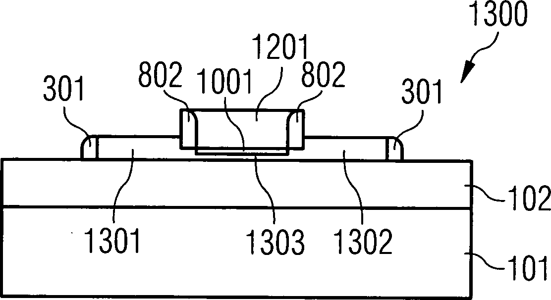
Bei
dem Feldeffekttransistor
In diesem Dokument sind folgende Veröffentlichungen zitiert:
- [1] T. Yonehara and K. Sakaguchi, "ELTRAN®; Novel SOI Wafer Technology", JSAP International No. 4 (July 2001), pp. 10–16
- [2]
DE 102 33 663 A1 - [3] G. Raghavan, J. L. Hoyt and J. F. Gibbons, Jpn. J. Appl. Phys., Vol. 32 (1993), pp. 380–383
- [4]
US 2003/0189231 A1
- [1] T. Yonehara and K. Sakaguchi, "ELTRAN ®; Novel SOI wafer technology", JSAP International No. 4 (July 2001), pp. 10-16
- [2]
DE 102 33 663 A1 - [3] G. Raghavan, JL Hoyt and JF Gibbons, Jpn. J. Appl. Phys., Vol. 32 (1993), pp. 380-383
- [4]
US 2003/0189231 A1
Claims (15)
Priority Applications (2)
| Application Number | Priority Date | Filing Date | Title |
|---|---|---|---|
| DE102004030552A DE102004030552B4 (en) | 2004-06-24 | 2004-06-24 | Layer arrangement, field effect transistor and method for producing a layer arrangement |
| PCT/DE2005/001095 WO2006000189A1 (en) | 2004-06-24 | 2005-06-20 | Layer assembly, field effect transistor, and method for producing a layer assembly |
Applications Claiming Priority (1)
| Application Number | Priority Date | Filing Date | Title |
|---|---|---|---|
| DE102004030552A DE102004030552B4 (en) | 2004-06-24 | 2004-06-24 | Layer arrangement, field effect transistor and method for producing a layer arrangement |
Publications (2)
| Publication Number | Publication Date |
|---|---|
| DE102004030552A1 DE102004030552A1 (en) | 2006-02-02 |
| DE102004030552B4 true DE102004030552B4 (en) | 2008-12-24 |
Family
ID=35058200
Family Applications (1)
| Application Number | Title | Priority Date | Filing Date |
|---|---|---|---|
| DE102004030552A Expired - Fee Related DE102004030552B4 (en) | 2004-06-24 | 2004-06-24 | Layer arrangement, field effect transistor and method for producing a layer arrangement |
Country Status (2)
| Country | Link |
|---|---|
| DE (1) | DE102004030552B4 (en) |
| WO (1) | WO2006000189A1 (en) |
Families Citing this family (1)
| Publication number | Priority date | Publication date | Assignee | Title |
|---|---|---|---|---|
| US7978504B2 (en) * | 2008-06-03 | 2011-07-12 | Infineon Technologies Ag | Floating gate device with graphite floating gate |
Citations (2)
| Publication number | Priority date | Publication date | Assignee | Title |
|---|---|---|---|---|
| US20030189231A1 (en) * | 1999-07-28 | 2003-10-09 | Clevenger Lawrence A. | Method and structure for providing improved thermal conduction for silicon semiconductor devices |
| DE10233663A1 (en) * | 2002-07-24 | 2004-02-19 | Infineon Technologies Ag | Production of a SOI substrate comprises preparing a SOI substrate by embedding a trenched oxide layer between a crystalline silicon layer and a silicon substrate |
Family Cites Families (4)
| Publication number | Priority date | Publication date | Assignee | Title |
|---|---|---|---|---|
| JPH04142079A (en) * | 1990-10-02 | 1992-05-15 | Nippon Telegr & Teleph Corp <Ntt> | Semiconductor device and manufacture thereof |
| JP2001352058A (en) * | 2000-06-09 | 2001-12-21 | Toshiba Corp | Method for manufacturing semiconductor device |
| US6566198B2 (en) * | 2001-03-29 | 2003-05-20 | International Business Machines Corporation | CMOS structure with non-epitaxial raised source/drain and self-aligned gate and method of manufacture |
| US7064050B2 (en) * | 2003-11-28 | 2006-06-20 | International Business Machines Corporation | Metal carbide gate structure and method of fabrication |
-
2004
- 2004-06-24 DE DE102004030552A patent/DE102004030552B4/en not_active Expired - Fee Related
-
2005
- 2005-06-20 WO PCT/DE2005/001095 patent/WO2006000189A1/en not_active Ceased
Patent Citations (2)
| Publication number | Priority date | Publication date | Assignee | Title |
|---|---|---|---|---|
| US20030189231A1 (en) * | 1999-07-28 | 2003-10-09 | Clevenger Lawrence A. | Method and structure for providing improved thermal conduction for silicon semiconductor devices |
| DE10233663A1 (en) * | 2002-07-24 | 2004-02-19 | Infineon Technologies Ag | Production of a SOI substrate comprises preparing a SOI substrate by embedding a trenched oxide layer between a crystalline silicon layer and a silicon substrate |
Non-Patent Citations (2)
| Title |
|---|
| RAGHAVAN, G. et al.: Polycrystalline Carbon: A Novel Material for Gate Electrodes in MOS Techno- logy. In: Jpn. J. Appl. Phys. Vol. 32(1993), S. 380-383 |
| RAGHAVAN, G. et al.: Polycrystalline Carbon: A Novel Material for Gate Electrodes in MOS Technology. In: Jpn. J. Appl. Phys. Vol. 32(1993), S. 380-383 * |
Also Published As
| Publication number | Publication date |
|---|---|
| DE102004030552A1 (en) | 2006-02-02 |
| WO2006000189A1 (en) | 2006-01-05 |
Similar Documents
| Publication | Publication Date | Title |
|---|---|---|
| DE112012001742B4 (en) | SEMICONDUCTOR STRUCTURE WITH A GRAPHENNANOBAND AND METHOD OF MANUFACTURING IT | |
| TWI306632B (en) | Methods for forming a semiconductor device | |
| DE112011102840B4 (en) | Semiconductor that is strained by elastic edge relaxation of a stressor in combination with a buried insulating layer | |
| DE102012206478B4 (en) | Extremely thin semiconductor on insulator (ETSOI) FET with a back gate and reduced parasitic capacitance, and method of making same | |
| DE112011100326B4 (en) | P-FET with a strained nanowire channel and embedded SiGe source and drain stressors and methods | |
| KR100903902B1 (en) | Non-planar mos structure with a strained channel region | |
| US7390707B2 (en) | Semiconductor device fabrication method | |
| CN101573795B (en) | Method for manufacturing semiconductor structure | |
| TWI230460B (en) | Gate-induced strain for MOS performance improvement | |
| DE112006001705B4 (en) | A method of fabricating an Integrated Complementary Metal Oxide Semiconductor Circuit using an elevated source drain and a replacement metal gate | |
| DE102005052054B4 (en) | Semiconductor device with shaped channel region transistors and method of making the same | |
| DE112007003116B4 (en) | Method for producing a strained transistor and transistor | |
| DE102012222116B4 (en) | Semiconductor structure with low equivalent oxide thickness double layer gate dielectric, graphene semiconductor devices and method | |
| US20090283842A1 (en) | Semiconductor device and method of fabricating the same | |
| TW201034084A (en) | Optimized compressive SiGe channel PMOS transistor with engineered Ge profile and optimized silicon cap layer | |
| DE112011101378T5 (en) | Epitaxy of delta monolayer dopants for embedded source / drain silicide | |
| WO2008054967A2 (en) | Method for providing a nanoscale, high electron mobility transistor (hemt) on insulator | |
| CN1914718A (en) | Method for forming a semiconductor device with local semiconductor-on-insulator | |
| US7033869B1 (en) | Strained silicon semiconductor on insulator MOSFET | |
| DE102010002450A1 (en) | Transistors with large gate metal gate electrode structures and matched channel semiconductor materials | |
| DE112006003576B4 (en) | A method of forming a FET having structure for reducing the external resistance of the three-dimensional transistor by using epitaxial layers and transistor | |
| DE102009023237A1 (en) | Deformation transformation in biaxially deformed SOI substrates to increase the performance of p-channel and n-channel transistors | |
| DE102008044983B4 (en) | Method for producing a structured deformed substrate, in particular for producing deformed transistors with a smaller thickness of the active layer | |
| DE102011080438B3 (en) | A manufacturing method of an N-channel transistor having a large-gate metal gate electrode structure and a reduced series resistance by epitaxially-fabricated semiconductor material in the drain and source regions and N-channel transistor | |
| DE112004002634B4 (en) | Integrated circuit, integrated circuit fabrication method, and method of making shallow trench isolation structures |
Legal Events
| Date | Code | Title | Description |
|---|---|---|---|
| OP8 | Request for examination as to paragraph 44 patent law | ||
| 8127 | New person/name/address of the applicant |
Owner name: QIMONDA AG, 81739 MUENCHEN, DE |
|
| 8364 | No opposition during term of opposition | ||
| R081 | Change of applicant/patentee |
Owner name: INFINEON TECHNOLOGIES AG, DE Free format text: FORMER OWNER: QIMONDA AG, 81739 MUENCHEN, DE Owner name: POLARIS INNOVATIONS LTD., IE Free format text: FORMER OWNER: QIMONDA AG, 81739 MUENCHEN, DE |
|
| R081 | Change of applicant/patentee |
Owner name: POLARIS INNOVATIONS LTD., IE Free format text: FORMER OWNER: INFINEON TECHNOLOGIES AG, 85579 NEUBIBERG, DE |
|
| R119 | Application deemed withdrawn, or ip right lapsed, due to non-payment of renewal fee |