CN2569518Y - General cripping device for print circuit board - Google Patents
General cripping device for print circuit board Download PDFInfo
- Publication number
- CN2569518Y CN2569518Y CN 02254893 CN02254893U CN2569518Y CN 2569518 Y CN2569518 Y CN 2569518Y CN 02254893 CN02254893 CN 02254893 CN 02254893 U CN02254893 U CN 02254893U CN 2569518 Y CN2569518 Y CN 2569518Y
- Authority
- CN
- China
- Prior art keywords
- crimping
- support column
- circuit board
- positioning
- cushion block
- Prior art date
- Legal status (The legal status is an assumption and is not a legal conclusion. Google has not performed a legal analysis and makes no representation as to the accuracy of the status listed.)
- Expired - Fee Related
Links
Images


Abstract
The utility model discloses a general compression joint device for printed circuit boards, which comprises a base board, a positioning pin positioned on the base board, a support column and a compression joint cushion block, wherein a plurality of unidiameter positioning and connecting screw holes are uniformly distributed on the base board, and the bottoms of the positioning pin, the support column and the compression joint cushion block are provided with positioning and connecting devices. The utility model also comprises a positioning and fixing device which is connected with the positioning and connecting screw holes and can fix the positioning pin, the support column and the compression joint cushion block respectively on any position of the base board. The positioning and connecting structures are arranged on the positioning pin, the support column and the compression joint cushion block, a positioning device matched with the positioning and connecting structures is arranged on the base board, so the positioning pin, and the support column and the compression joint cushion block can be fixedly arranged in different positions of the base board for supporting circuit boards according to the compression joint position change of the compression joint pieces of different circuit boards. The utility model has the advantages of low cost, strong universality, etc., and can save the design cost and the manufacture cost of a compression joint backing board; simultaneously, the occupation area for storing the special compression joint backing board and the handling cost can also be saved.
Description
Technical field
The utility model relates to the electronic product assembly tooling, is specifically related to a kind of general compression bonding apparatus that multiple printed circuit board carries out crimping dress connection that can be used for.
Background technology
In electronics, communications industry, crimping is a kind of typical electronic dress connection mode, and the crimping principle is a kind of connection that is formed with the cooperation of printed circuit board plated-through hole by the elastically deformable stitch of crimping device or rigidity stitch.Between contact pin and plated-through hole, form contact point closely, realize electric interconnection by mechanical connection.Cooperate in order to form closely, the cross sectional dimensions of stitch must be greater than printed circuit board plated-through hole aperture, in the crimping process, stitch cross section or plated-through hole will produce distortion, contact pin has two kinds of structures, a kind of is the rigidity contact pin: do not produce distortion in the crimping process, and the printed circuit board plated-through hole can be out of shape.Because of tolerance strictness, eliminate printed circuit board metallization aperture.Another kind is flexible contact pin: can be squeezed in the crimping process and be out of shape, and the printed circuit board plated-through hole is indeformable.
Most of connectors in the existing electronic product are exactly that mode by crimping is installed to printed circuit board, comprise on veneer and the backboard, in product, the crimping device both may be installed in the end face of printed circuit board, also may be installed in the bottom surface of printed circuit board, perhaps the two sides needs to install the crimping device simultaneously, but no matter be mounted in the side, all need to support the another side of printed circuit board, the hypothesis device is installed in the end face of printed circuit board now, and need support the bottom surface at printed circuit board this moment, to increase the rigidity of printed circuit board, prevent that printed circuit board is in distortion of crimping process even fracture, when providing support, also need to avoid crimping device stitch and pass printed circuit board, the bottom surface go out pin, and and the bottom surface on other devices of installing, such as electric capacity, resistance etc.;
Support the mode that printed circuit board carries out crimping in the prior art and mainly contain following two kinds:
1, utilize automatic crimping machine to realize crimping of crimping device and support printed circuit board simultaneously, its principle more complicated, be to utilize computer, control its crimping patrix and support bed die by the form of programming, utilize automatic crimping machine to realize crimping of crimping device and support printed circuit board simultaneously, its principle more complicated, to guarantee when the crimping patrix crimping device, supporting bed die just is supported under the printed circuit board that is crimped below the device, after having pressed a device, the crimping patrix is mentioned, then according to computer program instructions move another crimping device directly over, prepare crimping next time.In this process, support bed die and sink simultaneously, equally according to computer program instructions move another crimping device under, ascending branch props up printed circuit board then, prepares crimping next time, so the crimping of all crimping devices is finished in circulation.
2, be every kind of Printed Circuit Board Design, make special-purpose crimping backing plate, the schematic diagram when Fig. 1,2,3,4 is depicted as the special-purpose crimping backing plate of a kind of veneer wherein and supports veneer;
The hole is used in non-crimping device assembling on the special-purpose crimping backing plate general using printed circuit board, as screw hole as location hole, design plural alignment pin 1, be used for locating veneer, for there not being the appropriate bore can be, can realize purpose spacing and that support with the limit that guide vane end stop with the level supports printed circuit board as the printed circuit board of crimping backing plate location hole.Step surface on the alignment pin 1, support column 4 end faces and crimping cushion block 3 end face coplanes, and be fixed on the base plate 2 together support at the reverse side of printed circuit board, guaranteeing that printed circuit board keeps level, and avoid reverse side device 7, prevent that bottom surface device 7 is stressed and damage in the crimping process.Be drilled with aperture on the crimping cushion block, the hole that crimping device 6 is installed on the position of aperture and the printed circuit board is corresponding one by one, to avoid the pin that goes out that crimping device stitch passes printed circuit board.By above-mentioned measure, when crimping assembling crimping device 6, just can increase the printed circuit board rigidity, prevent that printed circuit board is out of shape or damages in the crimping process, prevent printed circuit board bottom surface device 7 stressed damage in the crimping process simultaneously, guaranteed crimp quality.
Fig. 4 places schematic diagram when carrying out crimping on its special-purpose crimping backing plate with printed circuit board.
There is following shortcoming in above-mentioned two kinds of crimping schemes:
The automaticity height of scheme 1, the equipment price costliness, the maintenance cost height requires height to operating personnel;
Scheme 2 is crimping support schemes that domestic most of electronics, communication enterprise adopt.Because the size of different printed circuit boards, location hole, the position of crimping device, the bottom surface device that need avoid etc. are had any different, need be at the special-purpose crimping backing plate of every kind of Printed Circuit Board Design, so just need the many and crimping backing plate that continue to increase of number to come corresponding to different printed circuit boards, increase the management cost of design cost, processing cost and crimping backing plate, also increased cost of goods manufactured.Simultaneously because the uncertainty of crimping backing plate in design, manufacturing process also may cause the product process-cycle to be incured loss through delay.
The utility model content
The technical problems to be solved in the utility model is, at above-mentioned shortcoming of the prior art, provide a kind of printed circuit board general compression bonding apparatus, this compression bonding apparatus can support different printed circuit boards and carry out crimping, cost-saved, overcome the product process-cycle delay that causes because of the uncertainty of crimping backing plate in design, manufacturing process simultaneously.
The technical scheme that the utility model provides is: design the general compression bonding apparatus of a kind of printed circuit board, comprise substrate, be positioned at alignment pin, support column and crimping cushion block on this substrate, on described substrate, be evenly equipped with a plurality of isodiametric screws that are located by connecting, the bottom of described alignment pin, support column and crimping cushion block is provided with locating connector, also comprise with the described screw that is located by connecting being connected, described alignment pin, support column and crimping cushion block can be fixed on the device for positioning and securing on the arbitrary position of described substrate.
In above-mentioned general compression bonding apparatus, described locating connector comprises the supporting bracket that is connected with described alignment pin, support column, described supporting bracket is provided with the locating interface groove of crisscross distribution, the supporting bracket that is connected with described crimping backing plate, on the location-plate of crimping cushion block both sides, be provided with the locating interface groove, described positioner comprises location-plate, and the front end of this location-plate is provided with the locator card joint that matches with described interface slot, also is provided with the connection location notch that can pass screw on location-plate.
The compression bonding apparatus that adopts the utility model to provide carries out the crimping assembling to circuit board, by at alignment pin, the structure that is located by connecting is set on support column and the crimping backing plate, the positioner that uses with the respective outer side edges that is located by connecting is set on substrate, can be according to the variation of various boards crimp crimping position, with alignment pin, the different parts that support column and crimping cushion block the are fixedly installed on substrate support circuit plate that gets on, compare with existing automatic crimping machine and special-purpose crimping backing plate, the utlity model has with low cost, to operating personnel require low, highly versatile, can save crimping backing plate design cost, the manufacturing cost management cost can be saved and be used for storing the occupation of land of special-purpose crimping backing plate and the advantages such as management cost of special-purpose crimping backing plate simultaneously.
Description of drawings
Fig. 1 is the special-purpose compression bonding apparatus front view of available circuit plate;
Fig. 2 is the left view of compression bonding apparatus shown in Figure 1;
Fig. 3 is the right view of compression bonding apparatus shown in Figure 1;
Fig. 4 is the schematic diagram when adopting special-purpose compression bonding apparatus shown in Figure 1 that circuit board is carried out crimping;
Fig. 5 is the general compression bonding apparatus structure of a utility model perspective view;
Fig. 6 is the front view of crimping cushion block in the compression bonding apparatus shown in Figure 5;
Fig. 7 is the left view of crimping cushion block shown in Figure 6;
Fig. 8 is the front view of crimping substrate in the compression bonding apparatus shown in Figure 5;
Fig. 9 is the front view of alignment pin in the compression bonding apparatus shown in Figure 5;
Figure 10 is an alignment pin left view shown in Figure 9;
Figure 11 is an alignment pin vertical view shown in Figure 9;
Figure 12 is a reference column front view in the compression bonding apparatus shown in Figure 5;
Figure 13 is a reference column left view shown in Figure 9;
Figure 14 is a reference column vertical view shown in Figure 9;
Figure 15 is the front view of positioner in the compression bonding apparatus shown in Figure 5;
Figure 16 is the vertical view of positioner shown in Figure 15.
Figure 17 is the front view that is used for compression bonding apparatus shown in Figure 5 limit locating piece;
Figure 18 is a limit shown in Figure 17 locating piece vertical view;
Embodiment
As shown in Figure 5, the general compression bonding apparatus of printed circuit board that provides by the utility model, on former dedicated substrate 11, be evenly equipped with a plurality of isodiametric screws that are located by connecting, at former alignment pin 15, the bottom of support column 8 and crimping cushion block 14 is provided with locating connector, other is provided with and a kind ofly can be connected screw connection with substrate 11 location of taking up an official post, with alignment pin 15, support column 8 and crimping cushion block 14 are fixed on the device for positioning and securing 9 on the arbitrary position of substrate, by this device for positioning and securing 9 moving on substrate 11, can change alignment pin 15, support column 8 and the Support Position of crimping cushion block 14 on substrate 11, thereby satisfy the crimping needs of various boards, further specify the concrete structure of each parts in the device below:
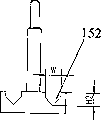
The concrete structure of crimping cushion block 14 such as Fig. 6, shown in Figure 7, be provided with supporting bracket 143 in the bottom of crimping backing plate 14, on the location-plate 143 of crimping cushion block 14 both sides, be provided with locating interface groove 141,142, locating interface groove 141, the V-shaped structure of 142 cross section, can be at every kind of crimping designs crimping cushion block, its effect is to support the position that needs crimping assembling crimping device on the printed circuit board, and avoid the crimping device and go out pin and be arranged on the substrate, the crimping cushion block can adopt one also can adopt the different cushion block 12 of a plurality of supporting surface structures according to different board structure of circuit, 13,14 come the support circuit plate, as shown in Figure 5,2mm connector (crimping device) with 5X25 PIN is an example, and the version of crimping cushion block is described;
Avoiding the position that crimping device contact pin goes out the pin hole on a, the various crimping cushion block decides according to the distribution of crimping device stitch, the aperture requires: the pad diameter>aperture of plated-through hole>stitch goes out the largest cross-sectional sized of foot section, requirement is less than or equal to the silk-screen width of crimping device on printed circuit board and half of the difference of W1, be less than or equal to the silk-screen length of crimping device on printed circuit board and half of the difference of L, if the crimping device needs splicing, requirement equals half of vertical pitch-row, and the degree of depth in hole requires to go out greater than crimping device contact pin the length of pin;
The height H 1 of b, various crimping cushion blocks is identical, and requires the maximum height greater than the printed circuit board device;
The interface slot cross sectional shape of c, various crimping cushion blocks is identical, i.e. the angle of W2, H2 and V-shaped groove requirement is same size.
The structure of substrate 11 requires the maximum overall dimension of the overall dimension of substrate 11 greater than the printed circuit board of band crimping as shown in Figure 8, and substrate equal intervals ground omnidirectional distribution diameter is screw 111 in the same manner.The effect of substrate 11 is to be used for fixing parts such as crimping cushion block 14, alignment pin 15, support column 8, device for positioning and securing 9 platform is provided.
The concrete structure of alignment pin 15, support column 8 such as Fig. 9-shown in Figure 14, be provided with 4 and be the locating interface groove 151,152,81,82 that intersecting parallels is interspersed on the supporting bracket 153,83 of alignment pin 15, support column 8, alignment pin 15, support column 8 are positioned at the center that is the locating interface groove that intersecting parallels is interspersed.
The version of alignment pin 15 and support column 8 is basic identical, unique difference is that alignment pin 15 has more a step axle than support column 8, the purposes of alignment pin 15 is to utilize screw hole or the rivet hole location of supporting on the printed circuit board and support printed circuit board, and the purposes of support column 8 is to support printed circuit board; The structural requirement of alignment pin 15 and support column 8 is as follows:
The interface slot cross sectional shape of a, alignment pin 15 and support column 8 and the interface slot of crimping cushion block 14 are identical;
The height dimension and the crimping cushion block 14 of b, alignment pin 15 step surfaces and support column 8 end faces are highly identical;
The equal diameters of the diameter of c, alignment pin 15 and support column 8 requires less than the taboo cloth district diameter that is used as the screw hole of crimping location hole on the printed circuit board, generally between 5~8mm;
The diameter of d, alignment pin 15 step axles must be less than the diameter that is used as the screw hole of crimping location hole on the printed circuit board, can will be used as the diameter classified statistics of the screw hole of crimping location hole on the printed circuit board, the diameter needles of alignment pin step axle is got a fixed value to every group.
The concrete structure of device for positioning and securing 9 is provided with location-plate shown in Figure 15,16, the front end of this location-plate is provided with the locator card joint 91 that matches with interface slot, also is provided with the connection location notch 92 that can pass screw on location-plate.Its purposes is by screw device for positioning and securing 9 to be fixed to optional position on the substrate 11, utilize device for positioning and securing 9 to push down crimping cushion block 14 or alignment pin 15 or support column 8, so just parts such as crimping cushion block 14, alignment pin 15, support column 8 can be fixed to the optional position on the machine plate.When being fastened to positioner 9 on the substrate with screw, before screw-driving, conduit on the location-plate can slide along screw, sliding distance equals the centre-to-centre spacing of its deep gouge, because centre-to-centre spacing is greater than the pitch of holes of substrate 11 screws 111, device for positioning and securing is in any one position that can be fixed on the directions X between X1 and X1 and the deep gouge centre-to-centre spacing, when needs are fixed in other positions on the substrate directions X, such as X2, can select near the fastening and adjustment realization of the screwed hole of X2, by the aforesaid operations device for positioning and securing can mobile covered substrate directions X on all positions, general reason, with its revolve turn 90 degrees after, can also mobile covered substrate Y direction on all positions, as shown in Figure 8.
For the clamping that guarantees fixture 9 ends 91 can cooperate with the interface slot of parts such as crimping cushion block 14, alignment pin 15, support column 8, the W of the interface slot of parts such as the W '<crimping cushion block 14 at requirement clamping 91 position, alignment pin 15, support column 8, the angle of the angle<V-shaped groove of V-arrangement head, H2 '>H2.
When crimping, if when on printed circuit board, not having to be used as the hole of location, the utility model also provides a kind of limit locating piece 16 shown in Figure 17,18 to locate, end at limit locating piece 16 is provided with a back-up block 161, and the height of its height H 1 and crimping cushion block 14 and alignment pin 15 step surfaces, support column 8 apical side heights are identical.The centre-to-centre spacing span of the link slot 162 of limit locating piece 16 can be directly be fixed on optional position on the substrate 11 with screw with limit locating piece 16 between the centre-to-centre spacing of screw 111 on 1~2 times of substrate 11.
The adjustment and the using method of general compression bonding apparatus are as follows:
A, at concrete printed circuit board, selected two above location holes utilize positioner that corresponding alignment pin is fixed on the substrate, the location printed circuit board.For the printed circuit board that does not have location hole, selected its three limits, the limit locating piece of employing more than three is fastened on locatees printed circuit board on the substrate;
B, find on the printed circuit board plated-through hole of assembling crimping device, utilize fine needle more than two to pass plated-through hole and locate corresponding crimping cushion block, utilize positioner and screw that the crimping cushion block is fastened on the substrate again;
C, at the large scale printed circuit board, in order to increase its rigidity, reduce distortion, the reverse side of selection printed circuit board crimping device fitting surface does not have the position of device, support printed circuit board with support column, and support column is fastened on the substrate with positioner and screw.
Repeat above-mentioned steps a~c when d, crimping difference veneer.
The general crimping backing plate of finally finishing assembling as shown in Figure 5.
Claims (8)
1, the general compression bonding apparatus of a kind of printed circuit board, comprise substrate (11), be positioned at the alignment pin (15) on this substrate (11), support column (8) and crimping cushion block (14), it is characterized in that, on described substrate (11), be evenly equipped with a plurality of isodiametric screws that are located by connecting (111), described alignment pin (15), the bottom of support column (8) and crimping cushion block (14) is provided with the locating connector that is supported on the described substrate (11), also comprise with the described screw that is located by connecting (111) being connected, described locating connector is fixed on device for positioning and securing (9) on the described substrate (11).
2, according to the described general compression bonding apparatus of claim 1, it is characterized in that, described locating connector comprises and described alignment pin (15), the supporting bracket (153 that support column (8) connects, 83), described supporting bracket is provided with the locating interface groove (151 of crisscross distribution, 152,81,82), the bottom of described crimping backing plate (14) is connected with supporting bracket (143), on the supporting bracket of crimping cushion block (14) both sides, be provided with locating interface groove (141,142), described device for positioning and securing (9) comprises location-plate, the front end of this location-plate is provided with and described interface slot (151,152,81,82,141,142) the locator card joint (91) that matches also is provided with the connection location notch (92) that can pass screw on location-plate.
According to the described general compression bonding apparatus of claim 2, it is characterized in that 3, a plurality of screws that are located by connecting (111) on the described substrate (11) adopt the mode of equidistant omnidirectional distribution to be provided with.
4, according to the described general compression bonding apparatus of claim 2, it is characterized in that, the supporting bracket of described alignment pin (15), support column (8) is provided with 4 and is the locating interface groove that intersecting parallels is interspersed, and described alignment pin (15), support column (8) are positioned at the described centre that is the locating interface groove that intersecting parallels is interspersed.
5, according to the described general compression bonding apparatus of claim 1, it is characterized in that, also comprise the limit locating piece (16) that is connected with the described screw that is located by connecting, described limit locating piece (16) comprises supporting seat, one end of described supporting seat is provided with upwardly extending back-up block (161), the end of this back-up block (161) is provided with the breach (163) with the board edge clamping, and described positioning seat is provided with and connects location notch (162).
According to claim 2 or 3 or 5 described general compression bonding apparatus, it is characterized in that 6, the length of described link slot is greater than the pitch of holes of the described screw that is located by connecting, the two ends of link slot are semicircular structure, are provided with the deep gouge that is used to hold head of screw in the described link slot.
7, according to claim 2 or 5 described general compression bonding apparatus, it is characterized in that the V-shaped structure of cross section of described locating interface groove and locator card joint.
8, according to claim 1 or 2 described general compression bonding apparatus, it is characterized in that, on described substrate, be provided with a crimping backing plate or an a plurality of crimping backing plate that is supported on the back of circuit board different parts respectively that is supported on the back of circuit board.
Priority Applications (1)
| Application Number | Priority Date | Filing Date | Title |
|---|---|---|---|
| CN 02254893 CN2569518Y (en) | 2002-09-23 | 2002-09-23 | General cripping device for print circuit board |
Applications Claiming Priority (1)
| Application Number | Priority Date | Filing Date | Title |
|---|---|---|---|
| CN 02254893 CN2569518Y (en) | 2002-09-23 | 2002-09-23 | General cripping device for print circuit board |
Publications (1)
| Publication Number | Publication Date |
|---|---|
| CN2569518Y true CN2569518Y (en) | 2003-08-27 |
Family
ID=33723539
Family Applications (1)
| Application Number | Title | Priority Date | Filing Date |
|---|---|---|---|
| CN 02254893 Expired - Fee Related CN2569518Y (en) | 2002-09-23 | 2002-09-23 | General cripping device for print circuit board |
Country Status (1)
| Country | Link |
|---|---|
| CN (1) | CN2569518Y (en) |
Cited By (21)
| Publication number | Priority date | Publication date | Assignee | Title |
|---|---|---|---|---|
| CN101393331B (en) * | 2008-11-04 | 2010-06-02 | 友达光电(苏州)有限公司 | Pressure bench structure and press joint device |
| CN101913007A (en) * | 2010-08-25 | 2010-12-15 | 武汉电信器件有限公司 | Device soft belt welding fixture |
| CN101668406B (en) * | 2008-09-01 | 2011-11-09 | 鸿富锦精密工业(深圳)有限公司 | Electronic device and support element thereof |
| CN102394589A (en) * | 2011-10-09 | 2012-03-28 | 台州雅晶电子有限公司 | Device used for positioning crystal oscillator and support |
| CN102751642A (en) * | 2012-05-17 | 2012-10-24 | 上海斐讯数据通信技术有限公司 | Optical line terminal (OLT) crimping device |
| CN104125717A (en) * | 2013-04-25 | 2014-10-29 | 雅马哈发动机株式会社 | Support pin, substrate support device, and substrate processing device |
| CN104812182A (en) * | 2014-01-23 | 2015-07-29 | 珠海格力电器股份有限公司 | Electric appliance box and air conditioner provided with same |
| CN104849507A (en) * | 2014-12-01 | 2015-08-19 | 重庆东登科技有限公司 | Test circuit board clamp |
| CN104849513A (en) * | 2014-12-03 | 2015-08-19 | 重庆东登科技有限公司 | Fixing clamp used for large-scale test circuit board |
| CN104849512A (en) * | 2014-12-03 | 2015-08-19 | 重庆东登科技有限公司 | Large-scale test circuit board fixing clamp |
| CN104849508A (en) * | 2014-12-01 | 2015-08-19 | 重庆东登科技有限公司 | Test circuit board fixing clamping mechanism |
| CN104849506A (en) * | 2014-12-01 | 2015-08-19 | 重庆东登科技有限公司 | Test circuit board clamping mechanism |
| CN104849511A (en) * | 2014-12-03 | 2015-08-19 | 重庆东登科技有限公司 | Portable test circuit board fixing clamp |
| CN104865413A (en) * | 2014-12-03 | 2015-08-26 | 重庆东登科技有限公司 | Fixing clamp for test circuit board |
| CN107196172A (en) * | 2017-05-27 | 2017-09-22 | 中国电子科技集团公司第四十研究所 | A kind of forced connector precision positioning compression bonding apparatus |
| CN107195574A (en) * | 2017-07-19 | 2017-09-22 | 广东工业大学 | A kind of ceramic substrate locating calibration device |
| CN110328627A (en) * | 2019-07-22 | 2019-10-15 | 中国电子科技集团公司第三十八研究所 | A kind of universal clipping tooling of printed circuit board |
| CN110614600A (en) * | 2019-01-14 | 2019-12-27 | 科大国盾量子技术股份有限公司 | Universal veneer crimping device and crimping method thereof |
| CN110719705A (en) * | 2018-07-11 | 2020-01-21 | 迈普通信技术股份有限公司 | Crimping die block |
| CN112103752A (en) * | 2020-08-30 | 2020-12-18 | 西南电子技术研究所(中国电子科技集团公司第十研究所) | VPX plug quick positioning crimping tool |
| CN115066084A (en) * | 2022-06-14 | 2022-09-16 | 一汽丰田汽车有限公司 | On-cable control box, mode two-charging connecting wire and on-cable control box detection method |
-
2002
- 2002-09-23 CN CN 02254893 patent/CN2569518Y/en not_active Expired - Fee Related
Cited By (32)
| Publication number | Priority date | Publication date | Assignee | Title |
|---|---|---|---|---|
| CN101668406B (en) * | 2008-09-01 | 2011-11-09 | 鸿富锦精密工业(深圳)有限公司 | Electronic device and support element thereof |
| CN101393331B (en) * | 2008-11-04 | 2010-06-02 | 友达光电(苏州)有限公司 | Pressure bench structure and press joint device |
| CN101913007A (en) * | 2010-08-25 | 2010-12-15 | 武汉电信器件有限公司 | Device soft belt welding fixture |
| CN102394589A (en) * | 2011-10-09 | 2012-03-28 | 台州雅晶电子有限公司 | Device used for positioning crystal oscillator and support |
| CN102394589B (en) * | 2011-10-09 | 2014-02-12 | 浙江雅晶电子有限公司 | Device used for positioning crystal oscillator and support |
| CN102751642A (en) * | 2012-05-17 | 2012-10-24 | 上海斐讯数据通信技术有限公司 | Optical line terminal (OLT) crimping device |
| CN104125717B (en) * | 2013-04-25 | 2017-03-29 | 雅马哈发动机株式会社 | Supporting pin, baseplate support device, substrate board treatment |
| CN104125717A (en) * | 2013-04-25 | 2014-10-29 | 雅马哈发动机株式会社 | Support pin, substrate support device, and substrate processing device |
| CN104812182A (en) * | 2014-01-23 | 2015-07-29 | 珠海格力电器股份有限公司 | Electric appliance box and air conditioner provided with same |
| CN104812182B (en) * | 2014-01-23 | 2018-07-13 | 珠海格力电器股份有限公司 | Electrical appliance kit and air conditioner with the electrical appliance kit |
| CN104849506B (en) * | 2014-12-01 | 2017-10-13 | 重庆达标电子科技有限公司 | Test circuit board clamping mechanism |
| CN104849508B (en) * | 2014-12-01 | 2017-07-18 | 重庆市蓝源机械制造有限公司 | Test circuit plate fixes to clamp mechanism |
| CN104849506A (en) * | 2014-12-01 | 2015-08-19 | 重庆东登科技有限公司 | Test circuit board clamping mechanism |
| CN104849507A (en) * | 2014-12-01 | 2015-08-19 | 重庆东登科技有限公司 | Test circuit board clamp |
| CN104849508A (en) * | 2014-12-01 | 2015-08-19 | 重庆东登科技有限公司 | Test circuit board fixing clamping mechanism |
| CN104849507B (en) * | 2014-12-01 | 2017-07-25 | 重庆巴酷科技有限公司 | test circuit board clamp |
| CN104865413A (en) * | 2014-12-03 | 2015-08-26 | 重庆东登科技有限公司 | Fixing clamp for test circuit board |
| CN104849513B (en) * | 2014-12-03 | 2017-07-04 | 重庆常青藤机械有限公司 | For the stationary fixture of large test circuit board |
| CN104849512A (en) * | 2014-12-03 | 2015-08-19 | 重庆东登科技有限公司 | Large-scale test circuit board fixing clamp |
| CN104849511B (en) * | 2014-12-03 | 2017-07-25 | 重庆巴酷科技有限公司 | The stationary fixture of portable test circuit plate |
| CN104865413B (en) * | 2014-12-03 | 2017-09-19 | 傅筱萸 | The stationary fixture of test circuit plate |
| CN104849513A (en) * | 2014-12-03 | 2015-08-19 | 重庆东登科技有限公司 | Fixing clamp used for large-scale test circuit board |
| CN104849511A (en) * | 2014-12-03 | 2015-08-19 | 重庆东登科技有限公司 | Portable test circuit board fixing clamp |
| CN104849512B (en) * | 2014-12-03 | 2017-09-29 | 重庆达标电子科技有限公司 | The stationary fixture of large test circuit board |
| CN107196172A (en) * | 2017-05-27 | 2017-09-22 | 中国电子科技集团公司第四十研究所 | A kind of forced connector precision positioning compression bonding apparatus |
| CN107195574A (en) * | 2017-07-19 | 2017-09-22 | 广东工业大学 | A kind of ceramic substrate locating calibration device |
| CN110719705A (en) * | 2018-07-11 | 2020-01-21 | 迈普通信技术股份有限公司 | Crimping die block |
| CN110614600A (en) * | 2019-01-14 | 2019-12-27 | 科大国盾量子技术股份有限公司 | Universal veneer crimping device and crimping method thereof |
| CN110328627A (en) * | 2019-07-22 | 2019-10-15 | 中国电子科技集团公司第三十八研究所 | A kind of universal clipping tooling of printed circuit board |
| CN112103752A (en) * | 2020-08-30 | 2020-12-18 | 西南电子技术研究所(中国电子科技集团公司第十研究所) | VPX plug quick positioning crimping tool |
| CN112103752B (en) * | 2020-08-30 | 2022-01-07 | 西南电子技术研究所(中国电子科技集团公司第十研究所) | VPX plug quick positioning crimping tool |
| CN115066084A (en) * | 2022-06-14 | 2022-09-16 | 一汽丰田汽车有限公司 | On-cable control box, mode two-charging connecting wire and on-cable control box detection method |
Similar Documents
| Publication | Publication Date | Title |
|---|---|---|
| CN2569518Y (en) | General cripping device for print circuit board | |
| CN100338818C (en) | Connector for memory card and mobile phone with the connector | |
| CN1290228C (en) | Electric connector | |
| CN1168365C (en) | Conveyer for printed circuit board of surface installation mechine | |
| CN2749076Y (en) | Electric connector having different spaces between terminals | |
| CN2757135Y (en) | Detector for circuit board | |
| CN1111833A (en) | Pinned module | |
| CN1196396C (en) | Method and device for locating printed circuit board on a punching machine | |
| CN1248374C (en) | Electric connector | |
| US4340092A (en) | Methods of and apparatus for straightening backplane-supported pins | |
| CN1759640A (en) | Pcb connector | |
| CN210046356U (en) | Metal plate processing tool of bending | |
| CN2716834Y (en) | A fixture | |
| CN2574079Y (en) | Mainframe board testing clamp | |
| CN210807816U (en) | V of PCB makeup that board limit is not parallel and level cuts anchor clamps | |
| CN1203733C (en) | Solder-bearing wafer for use in soldering operations | |
| CN213400425U (en) | Lamp plate fixing tool | |
| CN215768878U (en) | A test jig for circuit board detects | |
| CN2798343Y (en) | Three in one connecting socket for electronic card connector | |
| CN2684416Y (en) | Fixing apparatus for connector | |
| CN219634117U (en) | General type benzene board send board device | |
| CN2524275Y (en) | Fixer assembly | |
| CN215845837U (en) | Novel numerical control drilling machine for circuit board production | |
| CN2694521Y (en) | Guiding connector | |
| CN215487495U (en) | Lead screw module capable of being assembled quickly |
Legal Events
| Date | Code | Title | Description |
|---|---|---|---|
| C14 | Grant of patent or utility model | ||
| GR01 | Patent grant | ||
| C17 | Cessation of patent right | ||
| CF01 | Termination of patent right due to non-payment of annual fee |
Granted publication date: 20030827 Termination date: 20100923 |