CN202495884U - Rectification and energy feedback device - Google Patents
Rectification and energy feedback device Download PDFInfo
- Publication number
- CN202495884U CN202495884U CN201220056931XU CN201220056931U CN202495884U CN 202495884 U CN202495884 U CN 202495884U CN 201220056931X U CN201220056931X U CN 201220056931XU CN 201220056931 U CN201220056931 U CN 201220056931U CN 202495884 U CN202495884 U CN 202495884U
- Authority
- CN
- China
- Prior art keywords
- pin
- resistance
- amplifier
- connect
- diode
- Prior art date
- Legal status (The legal status is an assumption and is not a legal conclusion. Google has not performed a legal analysis and makes no representation as to the accuracy of the status listed.)
- Expired - Fee Related
Links
- 238000001514 detection method Methods 0.000 claims abstract description 20
- 239000003990 capacitor Substances 0.000 claims description 46
- 230000000087 stabilizing effect Effects 0.000 claims description 12
- 101100109978 Arabidopsis thaliana ARP3 gene Proteins 0.000 claims description 9
- 101100427547 Saccharomyces cerevisiae (strain ATCC 204508 / S288c) ULS1 gene Proteins 0.000 claims description 9
- 101150117607 dis1 gene Proteins 0.000 claims description 9
- 230000001360 synchronised effect Effects 0.000 claims description 9
- 102100024359 Exosome complex exonuclease RRP44 Human genes 0.000 claims description 8
- 101000627103 Homo sapiens Exosome complex exonuclease RRP44 Proteins 0.000 claims description 8
- 230000015572 biosynthetic process Effects 0.000 claims description 4
- 239000013078 crystal Substances 0.000 claims description 4
- 101100163122 Arabidopsis thaliana ARPC2A gene Proteins 0.000 claims description 3
- 101100191082 Saccharomyces cerevisiae (strain ATCC 204508 / S288c) GLC7 gene Proteins 0.000 claims description 3
- 101100030351 Schizosaccharomyces pombe (strain 972 / ATCC 24843) dis2 gene Proteins 0.000 claims description 3
- 238000003745 diagnosis Methods 0.000 abstract description 2
- 238000000034 method Methods 0.000 abstract description 2
- 230000009466 transformation Effects 0.000 abstract 1
- 238000010586 diagram Methods 0.000 description 11
- 238000005516 engineering process Methods 0.000 description 2
- 102100029376 Cryptochrome-1 Human genes 0.000 description 1
- 101000919351 Homo sapiens Cryptochrome-1 Proteins 0.000 description 1
- 230000003321 amplification Effects 0.000 description 1
- 230000001276 controlling effect Effects 0.000 description 1
- 230000005611 electricity Effects 0.000 description 1
- 238000004134 energy conservation Methods 0.000 description 1
- 230000007613 environmental effect Effects 0.000 description 1
- 238000001914 filtration Methods 0.000 description 1
- 238000004519 manufacturing process Methods 0.000 description 1
- 238000005272 metallurgy Methods 0.000 description 1
- 238000003199 nucleic acid amplification method Methods 0.000 description 1
- 238000000819 phase cycle Methods 0.000 description 1
- 230000001105 regulatory effect Effects 0.000 description 1
- 230000002441 reversible effect Effects 0.000 description 1
- 238000005070 sampling Methods 0.000 description 1
Images


Landscapes
- Rectifiers (AREA)
Abstract
The utility model provides a rectification and energy feedback device, which comprises a power circuit used for providing a direct voltage, a main control circuit, an alternating-current incoming and outgoing line phase lack detection unit, a rectification and feedback current loop detection unit, an armature voltage detection and speed feedback unit, an alternating-current synchronization signal detection unit, a thyristor trigger pulse generation circuit, an external speed setting unit, and a human-computer interface circuit. The alternating-current incoming and outgoing line phase lack detection unit, the rectification and feedback current loop detection unit, the armature voltage detection and speed feedback unit, the alternating-current synchronization signal detection unit, the thyristor trigger pulse generation circuit, the external speed setting unit, and the human-computer interface circuit are respectively connected with the main control circuit, the power circuit and the alternating-current incoming and outgoing line phase lack detection unit are respectively connected with a three-phase power supply, a first current mutual inductor and a second current mutual inductor are connected with the rectification and feedback current loop detection unit respectively, the thyristor trigger pulse generation circuit is connected with a rectification and feedback circuit, and the armature voltage detection and speed feedback unit is connected with an output end. The rectification and energy feedback device of the utility model can realize the open loop and close loop control, logic operation, fault diagnosis, parameter presetting, states and failure display, and the like, and is capable of avoiding errors in the transformation process and interferences caused by fluctuations of load or power supply.
Description
Technical field
The utility model relates to a kind of.Particularly relate to and a kind ofly convert three-phase alternating current into voltage fixing galvanic rectification and energy back feed device.
Background technology
Tradition rectification and energy back feed device are to realize closed-loop control through detecting voltage, electric current and rotating speed, and this close-loop control mode has caused circuit and problems such as additional electrical structure complicacy, cost height.
Summary of the invention
The utility model technical problem to be solved is, a kind of direct voltage that is used to provide is provided, and convert three-phase alternating current into voltage fixing direct current, and inversion is the rectification and the energy back feed device that go in the unnecessary energy feedback grid.
The technical scheme that the utility model adopted is: a kind of rectification and energy back feed device; Include the power circuit that is used to provide direct voltage; Also be provided with main control circuit; The alternating current inlet wire outlet phase shortage detecting unit that links to each other with main control circuit respectively, rectification feedback electric current loop detecting unit, armature voltage detect with speed feedback unit, alternating voltage synchronous signal detection unit, thyristor trigger impulse and produce circuit, external speed is given cell and man-machine interface circuit; Wherein, Described power circuit also is connected three phase mains respectively with alternating current inlet wire outlet phase shortage detecting unit; Described rectification feedback electric current loop test section also connects first current transformer and second current transformer respectively, and described thyristor trigger impulse produces circuit and also connects the rectification feedback unit, and armature voltage detects and also is connected output with the speed feedback unit.
Described main control circuit includes the interconnective single-chip microcomputer U9 of single-chip microcomputer U8, and the single-chip microcomputer U7 and the crystal oscillating circuit that link to each other with single-chip microcomputer U8 respectively also are provided with the DC power supply circuit that DC power supply is provided to single-chip microcomputer U8.
Described alternating current inlet wire outlet phase shortage detecting unit includes the interface J2 that links to each other with three phase mains; 6 pin of said interface J2 are connected an end of first rectifier bridge of being made up of four diode D6, D7, D10, D11 successively with resistance R 20 through resistance R 18; 2 pin of interface J2 connect the other end of first rectifier bridge through resistance R 10; 4 pin of interface J2 are connected an end of second rectifier bridge of being made up of four diode D8, D9, D12, D13 successively with resistance R 21 through resistance R 19; 2 pin of interface J2 also connect the other end of second rectifier bridge through resistance R 11; Two other end of said first rectifier bridge connects the two ends of resistance R 14 and two inputs of the first photoelectrical coupler U12 respectively; The output of the said first photoelectrical coupler U12 connects 1 pin and the test point of resistance R 12, capacitor C 23, NAND gate U10A respectively, and two other end of said second rectifier bridge connects the two ends of resistance R 15 and two inputs of the second photoelectrical coupler U13 respectively, and the output of the said second photoelectrical coupler U13 connects 2 pin of resistance R 13, capacitor C 24 and NAND gate U10A; The other end ground connection of said test point, capacitor C 23 and capacitor C 24; Another termination power VCC of resistance R 12 and resistance R 13,3 pin of NAND gate U10A connect 2 pin with door U11A, are connected 65 pin of the single-chip microcomputer U9 in the main control circuit with 1 pin of door U11A; 5 pin that are connected amplifier U14A with 3 pin of door U11A; 4 pin of amplifier U14A connect the 15V power supply through resistance R 16 respectively, and through resistance R 17 ground connection, output 2 pin of amplifier U14A connect 2 pin of the single-chip microcomputer U9 in the main control circuit.
Described rectification feedback electric current loop detecting unit (4) comprising: the 4th rectifier bridge that the 3rd rectifier bridge of being made up of diode D14, D15, D17, D18, D20, D21 and diode D16, D25, D19, D26, D22, D27 form; The input of described the 3rd rectifier bridge and the 4th rectifier bridge is connected current transformer through interface J3 with interface J4 respectively; The output of the 3rd rectifier bridge connects an end of diode D23, resistance R 34, resistance R 37 and resistance R 42 respectively; The other end of diode D23 links to each other with the end of voltage stabilizing didoe D28, and this link is through resistance R 35 connection+15V, the other end ground connection of voltage stabilizing didoe D28, resistance R 34 and resistance R 37; The other end of resistance R 42 connects 25 pin of single-chip microcomputer U17; And through capacitor C 25 ground connection, the output of the 4th rectifier bridge connects an end of diode D24, resistance R 39, resistance R 41 and resistance R 44 respectively, and the other end of diode D24 links to each other with the end of voltage stabilizing didoe D29; This link is through resistance R 36 connection+15V; The other end ground connection of voltage stabilizing didoe D29, resistance R 39 and resistance R 41, the other end of resistance R 44 connect 26 pin of single-chip microcomputer U17, and through capacitor C 27 ground connection; 2 pin of said single-chip microcomputer U17 meet download port J5; 17 pin connect 10 pin of amplifier U15C, and output 8 pin of amplifier U15C are through 3 pin of resistance R 22 connection amplifier U16, and output 6 pin of amplifier U16 connect 2 pin of amplifier U15A through resistance R 25; This 6 pin also connects 2 pin of switch U18A; 1 pin of switch U18A connects 11 pin of single-chip microcomputer U8 in the main control circuit (2), and output 1 pin of amplifier U15A is through 6 pin of resistance R 27 connection amplifier U15B, and the pin of amplifier U15B connects 6 pin of single-chip microcomputer U8 in the main control circuit (2) through resistance R 33.
Described armature voltage detects and comprises being useful on the speed feedback unit and be connected the interface J6 that rectification and energy back feed device voltage are exported; 1 pin of said interface J6 is connected 6 pin of amplifier U19B successively with resistance R 64 through resistance R 55, R57, R59, R61; 3 pin of said interface J6 connect 5 pin of amplifier U19B successively through the resistance R 65 of resistance R 56, R58, R60, R62, output 7 pin of amplifier U19B are through 2 pin of resistance R 67 connection amplifier U20A, the 3 pin ground connection of amplifier U20A; Export 1 pin formation speed feedback and connect capacitor C 41, resistance R 78 and resistance R 75 respectively; Capacitor C 41 other end ground connection, the other end of resistance R 75 are successively through potentiometer R68 and resistance R 72 ground connection, and the other end of resistance R 78 connects test point and resistance R 74 through resistance R 76; The other end of resistance R 74 connects the other end, the connection capacitor C 40 of test point respectively and constitutes subsequent use speed setting port through resistance R 73; The other end ground connection of capacitor C 40, the adjustable end of potentiometer R68 is through 10 pin of resistance R 77 connection amplifier U19C, and 9 pin of amplifier U19C connect output 8 pin through potentiometer R69 and resistance R 81 successively; Export 8 pin are connected amplifier U19A successively with resistance R 84 through resistance R 83 2 pin; 3 pin of amplifier U19A are exported 1 pin through capacitor C 42 ground connection through resistance R 71 ground connection, and connect 13 pin of amplifier U19D through resistance R 49; 12 pin of amplifier U19D are through resistance R 51 ground connection; Output 14 pin of amplifier U19D connect 5 pin of amplifier U20B through diode D30, and 6 pin of amplifier U20B connect 4 pin of single-chip microcomputer U8 in the main control circuit respectively, diode D31 and resistance R 52; The other end of said diode D31 connects output 7 pin of amplifier U20B, another termination VREF of resistance R 52.
Described alternating voltage synchronous signal detection unit includes amplifier U21B, amplifier U21A and amplifier U22; 6 pin of described amplifier U21B are connected the W1 end of three phase mains successively with resistance R 99 through resistance R 108, R105, R103, R101; 5 pin of amplifier U21B are connected the U1 end of three phase mains successively with resistance R 100 through resistance R 109, R106, R104, R102; Output 7 pin of amplifier U21B connect diode D34, diode D35 and resistance R 85 respectively; The other end of diode D34 connects 3 pin of amplifier U21A through resistance R 87; The other end of diode D35 is through 2 pin of resistance R 88 connection amplifier U21A, and output 1 pin of amplifier U21A is connected 5 pin of single-chip microcomputer U8 in the main control circuit successively with resistance R 96 through resistance R 94, and the other end of said resistance R 85 is through capacitor C 55 ground connection; Also connect 3 pin of amplifier U22 through resistance R 89; 2 pin of U22 are through capacitor C 58 and 24 pin resistance R 93 and that connect single-chip microcomputer U8 in the main control circuit, and output 7 pin of amplifier U22 connect 24 pin of single-chip microcomputer U8 in the main control circuit, and this is exported 7 pin and also connects power supply VCC through resistance R 95.
Described thyristor trigger impulse produces circuit and includes chip for driving U23 and chip for driving U24, and 12 pulse transformer T1~T12, and 1~6 pin of wherein said chip for driving U23 is connected single-chip microcomputer U9 in the main control circuit respectively with 2~7 pin of chip for driving U24; Corresponding the elementary of pulse transformer T9, pulse transformer T1, pulse transformer T11, pulse transformer T10, pulse transformer T2 and pulse transformer T12, corresponding the elementary of pulse transformer T3, pulse transformer T7, pulse transformer T5, pulse transformer T4, pulse transformer T8 and pulse transformer T6, the secondary shunt capacitance C63 of said pulse transformer T1 of connecting of 10~15 pin of described chip for driving U24 of connecting of 11~16 pin of described chip for driving U23; Also connect output interface X2 through diode V7; The secondary shunt capacitance C64 of said pulse transformer T2 also connects output interface X2, the secondary shunt capacitance C65 of said pulse transformer T3 through diode V7; Also connect output interface X3 through diode V8; The secondary shunt capacitance C66 of said pulse transformer T4 also connects output interface X3, the secondary shunt capacitance C67 of said pulse transformer T5 through diode V5; Also connect output interface X4 through diode V9; The secondary shunt capacitance C68 of said pulse transformer T6 also connects output interface X4, the secondary shunt capacitance C69 of said pulse transformer T7 through diode V6; Also connect output interface X5 through diode V13; The secondary shunt capacitance C70 of said pulse transformer T8 also connects output interface X5, the secondary shunt capacitance C71 of said pulse transformer T9 through diode V10; Also connect output interface X6 through diode V14; The secondary shunt capacitance C72 of said pulse transformer T10 also connects output interface X5, the secondary shunt capacitance C73 of said pulse transformer T11 through diode V11; Also connect output interface X7 through diode V15; The secondary shunt capacitance C74 of said pulse transformer T12 also connects output interface X7 through diode V12, and described interface 2~interface 7 connects the rectification feedback unit respectively.
The given unit of described external speed includes amplifier U25A, amplifier U25B, amplifier U25C and amplifier U25D; 2 pin of said amplifier U25A are connected 7 pin and the external speed setting of single-chip microcomputer U8 in the main control circuit successively respectively through resistance R 133 and resistance R 132; And through capacitor C 75 ground connection; The tie point of resistance R 133 and resistance R 132 is ground connection also; 2 pin of amplifier U25A also connect 6 pin of amplifier U25B jointly respectively through resistance R 123 through resistance R 135 and output pin 1; Connect 13 pin of amplifier U25D through resistance R 127, the output pin 1 of described amplifier U25A also is connected 10 pin of amplifier U25C successively jointly through resistance R 123 and output 7 pin of resistance R 125 and amplifier U25B, and 3 pin of amplifier U25A are through resistance R 134 ground connection; 5 pin of amplifier U25B are through resistance R 124 ground connection; 12 pin of amplifier U25D also are connected diode D39 and diode D38 through resistance R 130,21 pin of single-chip microcomputer U8 in another termination main control circuit of diode D39 through resistance R 129 with output pin 14 jointly through resistance R 128 ground connection; The other end ground connection of diode D38,9 pin of amplifier U25C connect 7 pin of single-chip microcomputer U8 in the main control circuit respectively and connects external speed to be set.
Described man-machine interface circuit comprises drive circuit U26 and drive circuit U27; Charactron DIS1~charactron DIS3; 2 pin of said drive circuit U26 and drive circuit U27~9 pin are connected 60 pin~53 pin of single-chip microcomputer U8 in the main control circuit, and 12 pin of drive circuit U26~19 pin connect 10 pin, 9 pin, 7 pin, 5 pin, 4 pin, 2 pin, 1 pin and 6 pin of charactron DIS1~charactron DIS3 respectively through resistor chain RS1, and 12 pin of drive circuit U27 connect the base stage of triode T15 through resistance R 141; 13 pin connect the base stage of triode T14 through resistance R 139; 14 pin connect the base stage of triode T13 through resistance R 137, and 15 pin connect 11 pin of single-chip microcomputer U8 in the main control circuit, and 17 pin connect sets button K3; 18 pin connect sets button K2; 19 pin connect sets button K1, corresponding respectively pin 4, pin 3 and the pin 2 that is connected resistor chain RS2 of an end among described setting button K3, setting button K2 and the setting button K1, and the base stage of triode T13, triode T14 and triode T15 also respectively meets power supply VCC through a resistance; Collector electrode meets power supply VCC, 3 pin and 8 pin of connection charactron DIS1, charactron DIS2 and charactron DIS3 that emitter is corresponding.
Described rectification feedback unit includes three groups of rectifying part of identical in structure and three groups of feedback parts; Each group rectifying part or feedback part all are to be made up of two anti-parallel thyristor bridges; Wherein, Corresponding respectively three phase mains U1, V1, the W1 of connecting of the tie point of two anti-parallel thyristors of each group in three groups of rectifying part; Corresponding respectively three phase mains U2, V2, the W2 of connecting of the tie point of two thyristors of each group in three groups of feedbacks part; Described three phase mains U2, V2, W2 connect three phase mains through auto-transformer; Described three phase mains U1, V1, W1 directly connect three phase mains; In described three groups of rectifying part and the three groups of feedbacks part two ends of two thyristors of each group each corresponding through a current transformer to output voltage terminal, each the thyristor trigger end in said three groups of rectifying part connects the thyristor trigger impulse respectively and produces output interface X3, output interface X4 and output interface X5 in the circuit, each the thyristor trigger end in said three groups of feedbacks part connects the thyristor trigger impulse respectively and produces the output interface X2 in the circuit, the output interface X7 of output interface X6.
Rectification of the utility model and energy back feed device can be realized open loop, closed-loop control, logical operation; Failure diagnosis, preset parameter, state and fault demonstration etc.; It is reversible that ac equipment adopts the direct inverse parallel of thyristor not have circulation; Avoided the sum of errors in the transfer process because the interference that load or power supply fluctuation bring has not only improved modulation accuracy, and improved functional reliability and efficient; Be easy to realize the requirement of all kinds of manufacturing machine technologies, can extensively be used in industries such as metallurgy, mine, light industry, papermaking.Use this rectification feedback module more to help environmental protection and energy-conservation.
Description of drawings
Fig. 1 is the rectification of the utility model and the formation block diagram of energy back feed device;
Fig. 2 (a) provides the power circuit principle figure of direct voltage;
Fig. 2 (b) provides the circuit theory diagrams of the various DC power supplys that need in the work;
Fig. 3 is the circuit diagram of main control circuit;
Fig. 4 is the circuit theory diagrams of alternating current inlet wire outlet phase shortage detecting unit;
Fig. 5 is the circuit theory diagrams of rectification feedback electric current loop detecting unit;
Fig. 6 is the circuit theory diagrams of armature voltage detection and speed feedback unit;
Fig. 7 is the circuit theory diagrams of alternating voltage synchronous signal detection unit;
Fig. 8 is the circuit theory diagrams that the thyristor trigger impulse produces circuit;
Fig. 9 is the circuit theory diagrams that external speed is given cell;
Figure 10 is the circuit theory diagrams of man-machine interface circuit;
Figure 11 is the circuit theory diagrams of rectification feedback unit.
Wherein:
1: power circuit 2: main control circuit
3: alternating current inlet wire outlet phase shortage detecting unit 4: rectification feedback electric current loop detecting unit
5: armature voltage detects and speed feedback unit 6: the alternating voltage synchronous signal detection unit
7: the thyristor trigger impulse produces circuit 8: external speed is given cell
9: man-machine interface circuit 10: the rectification feedback unit
12: the second current transformers of 11: the first current transformers
Embodiment
Below in conjunction with embodiment and accompanying drawing the rectification and the energy back feed device of the utility model are made detailed description.
As shown in Figure 1; Rectification of the utility model and energy back feed device; Include the power circuit 1 that is used to provide direct voltage; Also be provided with main control circuit 2; The alternating current inlet wire outlet phase shortage detecting unit 3 that links to each other with main control circuit 2 respectively, rectification feedback electric current loop detecting unit 4, armature voltage detect with speed feedback unit 5, alternating voltage synchronous signal detection unit 6, thyristor trigger impulse and produce circuit 7, external speed is given cell 8 and man-machine interface circuit 9; Wherein, described power circuit 1 also is connected three phase mains respectively with alternating current inlet wire outlet phase shortage detecting unit 3, and described rectification feedback electric current loop test section 4 also connects first current transformer 11 and second current transformer 12 respectively; Described thyristor trigger impulse produces circuit 7 and also connects rectification feedback unit 10, and armature voltage detects and also is connected output C, D with speed feedback unit 5.
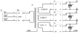
Shown in Fig. 2 (a), Fig. 2 (b), described dc power supply partial circuit 1 be by three-phase electricity wherein two do power supply mutually, insert J1; Connect to transformer S1 through electromagnetic interface filter FI1; Obtain alternating voltage, obtaining three DC power supplys through three rectifier bridge V1, V2, V3, DC power supply access power module U1, U2, U3, U4 obtain the various DC power supplys of needs in the work; Wherein also comprise the amplifier module U5A, U5B, U6A, the U6B that are used for rectification, filtering and amplification; Capacitor C 1~C19, resistance R 1~R8, inductance L 1.
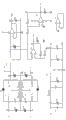
As shown in Figure 3; It is that the interconnective model of single-chip microcomputer U8 of 80C196KB is the single-chip microcomputer U9 of PSD4135 that described main control circuit 2 includes model; The model that links to each other with single-chip microcomputer U8 respectively is the single-chip microcomputer U7 of MAX707, by the crystal oscillating circuit that 16M crystal oscillator CRY1 and capacitor C 20 and capacitor C 21 are formed, also be provided with by what capacitor C 22, resistance R 9, diode D3~D5 and dry cell E formed and the DC power supply circuit of DC power supply be provided to single-chip microcomputer U8.
As shown in Figure 4; Described alternating current inlet wire outlet phase shortage detecting unit 3 includes the interface J2 that links to each other with three phase mains; 6 pin of said interface J2 are connected an end of first rectifier bridge of being made up of four diode D6, D7, D10, D11 successively with resistance R 20 through resistance R 18; 2 pin of interface J2 connect the other end of first rectifier bridge through resistance R 10; 4 pin of interface J2 are connected an end of second rectifier bridge of being made up of four diode D8, D9, D12, D13 successively with resistance R 21 through resistance R 19; 2 pin of interface J2 also connect the other end of second rectifier bridge through resistance R 11, two other end of said first rectifier bridge connects the two ends of resistance R 14 and two inputs of the first photoelectrical coupler U12 respectively, and the output of the said first photoelectrical coupler U12 connects 1 pin and the test point DS1 of resistance R 12, capacitor C 23, NAND gate U10A respectively; Two other end of said second rectifier bridge connects the two ends of resistance R 15 and two inputs of the second photoelectrical coupler U13 respectively; The output of the said second photoelectrical coupler U13 connects 2 pin of resistance R 13, capacitor C 24 and NAND gate U10A, the other end ground connection of said test point DS1, capacitor C 23 and capacitor C 24, another termination power VCC of resistance R 12 and resistance R 13; 3 pin of NAND gate U10A connect 2 pin with door U11A; 65 pin that are connected the single-chip microcomputer U9 in the main control circuit 2 with 1 pin of door U11A are connected 5 pin of amplifier U14A with 3 pin of door U11A, 4 pin of amplifier U14A connect the 15V power supply through resistance R 16 respectively; And through resistance R 17 ground connection, output 2 pin of amplifier U14A connect 2 pin of the single-chip microcomputer U9 in the main control circuit 2.
As shown in Figure 5; Described rectification feedback electric current loop detecting unit 4 comprises: the 4th rectifier bridge that the 3rd rectifier bridge of being made up of diode D14, D15, D17, D18, D20, D21 and diode D16, D25, D19, D26, D22, D27 form; The input of described the 3rd rectifier bridge and the 4th rectifier bridge is connected current transformer through interface J3 with interface J4 respectively, and the output of the 3rd rectifier bridge connects an end of diode D23, resistance R 34, resistance R 37 and resistance R 42 respectively, and the other end of diode D23 links to each other with the end of voltage stabilizing didoe D28; This link is through resistance R 35 connection+15V; The other end ground connection of voltage stabilizing didoe D28, resistance R 34 and resistance R 37, the other end of resistance R 42 connect 25 pin of single-chip microcomputer U17, and through capacitor C 25 ground connection; The output of the 4th rectifier bridge connects an end of diode D24, resistance R 39, resistance R 41 and resistance R 44 respectively; The other end of diode D24 links to each other with the end of voltage stabilizing didoe D29, and this link is through resistance R 36 connection+15V, the other end ground connection of voltage stabilizing didoe D29, resistance R 39 and resistance R 41; The other end of resistance R 44 connects 26 pin of single-chip microcomputer U17; And through capacitor C 27 ground connection, 2 pin of said single-chip microcomputer U17 meet download port J5, and 17 pin connect 10 pin of amplifier U15C; Output 8 pin of amplifier U15C connect 3 pin of amplifier U16 through resistance R 22; Output 6 pin of amplifier U16 are through 2 pin of resistance R 25 connection amplifier U15A, and this 6 pin also connects 2 pin of switch U18A, and 1 pin of switch U18A connects 11 pin of single-chip microcomputer U8 in the main control circuit 2; Output 1 pin of amplifier U15A is through 6 pin of resistance R 27 connection amplifier U15B, and the pin of amplifier U15B connects 6 pin of single-chip microcomputer U8 in the main control circuits 2 through resistance R 33.Handling to single-chip microcomputer U8 through amplifier U15, U16 through single-chip microcomputer U17 summation through sampling resistor R34, R37, R39, R41.
As shown in Figure 6; Described armature voltage detects with speed feedback unit 5 and includes the interface J6 that is used to be connected rectification and the output of energy back feed device voltage, and 1 pin of said interface J6 is connected 6 pin of amplifier U19B successively with resistance R 64 through resistance R 55, R57, R59, R61, and 3 pin of said interface J6 connect 5 pin of amplifier U19B successively through the resistance R 65 of resistance R 56, R58, R60, R62; Output 7 pin of amplifier U19B connect 2 pin of amplifier U20A through resistance R 67; The 3 pin ground connection of amplifier U20A are exported 1 pin formation speed feedback and are connected capacitor C 41, resistance R 78 and resistance R 75 respectively, capacitor C 41 other end ground connection; The other end of resistance R 75 is successively through potentiometer R68 and resistance R 72 ground connection; The other end of resistance R 78 connects test point BR1 and resistance R 74 through resistance R 76, and the other end of resistance R 74 connects the other end, the connection capacitor C 40 of test point BR1 respectively and constitutes subsequent use speed setting port, the other end ground connection of capacitor C 40 through resistance R 73; The adjustable end of potentiometer R68 connects 10 pin of amplifier U19C through resistance R 77; 9 pin of amplifier U19C connect output 8 pin through potentiometer R69 and resistance R 81 successively, export 8 pin are connected amplifier U19A successively with resistance R 84 through resistance R 83 2 pin, and 3 pin of amplifier U19A are through resistance R 71 ground connection; Export 1 pin through capacitor C 42 ground connection; And pass through 13 pin that resistance R 49 connects amplifier U19D, and 12 pin of amplifier U19D are through resistance R 51 ground connection, and output 14 pin of amplifier U19D connect 5 pin of amplifier U20B through diode D30; 6 pin of amplifier U20B connect 4 pin of single-chip microcomputer U8 in the main control circuit 2 respectively; Diode D31 and resistance R 52, the other end of said diode D31 connects output 7 pin of amplifier U20B, another termination VREF of resistance R 52.
As shown in Figure 7; Described alternating voltage synchronous signal detection unit 6 includes amplifier U21B, amplifier U21A and amplifier U22; 6 pin of described amplifier U21B are connected the W1 end of three phase mains successively with resistance R 99 through resistance R 108, R105, R103, R101; 5 pin of amplifier U21B are connected the U1 end of three phase mains successively with resistance R 100 through resistance R 109, R106, R104, R102; Output 7 pin of amplifier U21B connect diode D34, diode D35 and resistance R 85 respectively, and the other end of diode D34 is through 3 pin of resistance R 87 connection amplifier U21A, and the other end of diode D35 connects 2 pin of amplifier U21A through resistance R 88; Output 1 pin of amplifier U21A is connected 5 pin of single-chip microcomputer U8 in the main control circuit 2 successively with resistance R 96 through resistance R 94; The other end of said resistance R 85 also connects 3 pin of amplifier U22 through capacitor C 55 ground connection through resistance R 89,2 pin of U22 are through capacitor C 58 and 24 pin resistance R 93 and that connect single-chip microcomputer U8 in the main control circuit 2; Output 7 pin of amplifier U22 connect 24 pin of single-chip microcomputer U8 in the main control circuit 2, and this is exported 7 pin and also connects power supply VCC through resistance R 95.
As shown in Figure 8, described thyristor trigger impulse produces circuit 7 and includes chip for driving U23 and the chip for driving U24 that model is MC1413, and 12 pulse transformer T1~T12; 1~6 pin of wherein said chip for driving U23 is connected single-chip microcomputer U9 in the main control circuit 2 respectively with 2~7 pin of chip for driving U24, and the corresponding connection of 11~16 pin of described chip for driving U23 pulse transformer T9, pulse transformer T1, pulse transformer T11, pulse transformer T10, pulse transformer T2 and pulse transformer T12's is elementary, and the corresponding connection of 10~15 pin of described chip for driving U24 pulse transformer T3, pulse transformer T7, pulse transformer T5, pulse transformer T4, pulse transformer T8 and pulse transformer T6's is elementary; The secondary shunt capacitance C63 of said pulse transformer T1 also connects output interface X2, the secondary shunt capacitance C64 of said pulse transformer T2 through diode V7; Also connect output interface X2 through diode V7; The secondary shunt capacitance C65 of said pulse transformer T3 also connects output interface X3, the secondary shunt capacitance C66 of said pulse transformer T4 through diode V8; Also connect output interface X3 through diode V5; The secondary shunt capacitance C67 of said pulse transformer T5 also connects output interface X4, the secondary shunt capacitance C68 of said pulse transformer T6 through diode V9; Also connect output interface X4 through diode V6; The secondary shunt capacitance C69 of said pulse transformer T7 also connects output interface X5, the secondary shunt capacitance C70 of said pulse transformer T8 through diode V13; Also connect output interface X5 through diode V10; The secondary shunt capacitance C71 of said pulse transformer T9 also connects output interface X6, the secondary shunt capacitance C72 of said pulse transformer T10 through diode V14; Also connect output interface X5 through diode V11; The secondary shunt capacitance C73 of said pulse transformer T11 also connects output interface X7, the secondary shunt capacitance C74 of said pulse transformer T12 through diode V15; Also connect output interface X7 through diode V12, described interface 2~interface 7 connects rectification feedback unit 10 respectively.
As shown in Figure 9; Described external speed includes amplifier U25A, amplifier U25B, amplifier U25C and amplifier U25D for cell 8; 2 pin of said amplifier U25A are connected 7 pin and the external speed setting of single-chip microcomputer U8 in the main control circuit 2 successively respectively through resistance R 133 and resistance R 132; And through capacitor C 75 ground connection; The tie point of resistance R 133 and resistance R 132 is ground connection also, and 2 pin of amplifier U25A also connect 6 pin of amplifier U25B jointly respectively through resistance R 123 through resistance R 135 and output pin 1, connects 13 pin of amplifier U25D through resistance R 127; The output pin 1 of described amplifier U25A also is connected 10 pin of amplifier U25C successively jointly through resistance R 123 and output 7 pin of resistance R 125 and amplifier U25B; 3 pin of amplifier U25A are through resistance R 134 ground connection, and 5 pin of amplifier U25B are through resistance R 124 ground connection, and 12 pin of amplifier U25D are through resistance R 128 ground connection; Also be connected diode D39 and diode D38 through resistance R 130 jointly with output pin 14 through resistance R 129; 21 pin of single-chip microcomputer U8 in another termination main control circuit 2 of diode D39, the other end ground connection of diode D38,9 pin of amplifier U25C connect 7 pin of single-chip microcomputer U8 in the main control circuit 2 respectively and connect external speed to be set.
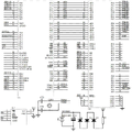
Shown in figure 10; Described man-machine interface circuit 9 comprises that model is drive circuit U26 and the drive circuit U27 of 74HC573; Model is charactron DIS1~charactron DIS3 of LA3911-11; 2 pin of said drive circuit U26 and drive circuit U27~9 pin are connected 60 pin~53 pin of single-chip microcomputer U8 in the main control circuit 2, and 12 pin of drive circuit U26~19 pin connect 10 pin, 9 pin, 7 pin, 5 pin, 4 pin, 2 pin, 1 pin and 6 pin of charactron DIS1~charactron DIS3 respectively through resistor chain RS1, and 12 pin of drive circuit U27 connect the base stage of triode T15 through resistance R 141; 13 pin connect the base stage of triode T14 through resistance R 139; 14 pin connect the base stage of triode T13 through resistance R 137, and 15 pin connect 11 pin of single-chip microcomputer U8 in the main control circuit 2, and 17 pin connect sets button K3; 18 pin connect sets button K2; 19 pin connect sets button K1, corresponding respectively pin 4, pin 3 and the pin 2 that is connected resistor chain RS2 of an end among described setting button K3, setting button K2 and the setting button K1, and the base stage of triode T13, triode T14 and triode T15 also respectively meets power supply VCC through a resistance; Collector electrode meets power supply VCC, 3 pin and 8 pin of connection charactron DIS1, charactron DIS2 and charactron DIS3 that emitter is corresponding.
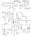
Described rectification feedback unit 10 is made up of two groups of identical anti-parallel thyristor bridges, be used for to inverter DC bus powered and by dc bus to the electrical network feedback energy.For fear of when feedback is worked, producing voltage drop, the input voltage of feedback must be high by 20%.This can realize that when not having high voltage on the feedback terminal, intermediate circuit voltage reduces through phase angle variations through the own electrical network of an auto-transformer or connection service bridge.Intermediate circuit voltage is regulated by the digital governer of a band microprocessor automatically.The utility model has control direct current electric source and ac synchronous input part through 6 group pulse signal controlling, is furnished with inlet wire feedback line phase sequence simultaneously and detects voltage detecting, current detecting.Output has voltage detecting, and capacitance-resistance absorbs filter circuit.
Shown in figure 11; Described rectification feedback unit 10 includes three groups of rectifying part of identical in structure and three groups of feedback parts; Each group rectifying part or feedback part all are to be made up of two anti-parallel thyristor bridges; Wherein, Corresponding respectively three phase mains U1, V1, the W1 of connecting of the tie point of two anti-parallel thyristors of each group in three groups of rectifying part; Corresponding respectively three phase mains U2, V2, the W2 of connecting of the tie point of two thyristors of each group in three groups of feedbacks part; Described three phase mains U2, V2, W2 connect three phase mains through auto-transformer 13, and described three phase mains U1, V1, W1 directly connect three phase mains, in described three groups of rectifying part and the three groups of feedback parts two ends of two thyristors of each group each corresponding through a current transformer 11,12 to output voltage terminal C, D; Each thyristor trigger end in said three groups of rectifying part connects the thyristor trigger impulse respectively and produces output interface X3, output interface X4 and output interface X5 in the circuit (7), and each the thyristor trigger end in said three groups of feedbacks part connects the thyristor trigger impulse respectively and produces the output interface X2 in the circuit 7, the output interface X7 of output interface X6.
Claims (10)
1. rectification and energy back feed device; Include the power circuit (1) that is used to provide direct voltage; It is characterized in that; Also be provided with main control circuit (2); The alternating current inlet wire outlet phase shortage detecting unit (3) that links to each other with main control circuit (2) respectively, rectification feedback electric current loop detecting unit (4), armature voltage detect with speed feedback unit (5), alternating voltage synchronous signal detection unit (6), thyristor trigger impulse and produce circuit (7), external speed is given cell (8) and man-machine interface circuit (9); Wherein, described power circuit (1) also is connected three phase mains respectively with alternating current inlet wire outlet phase shortage detecting unit (3), and described rectification feedback electric current loop test section (4) also connects first current transformer (11) and second current transformer (12) respectively; Described thyristor trigger impulse produces circuit (7) and also connects rectification feedback unit (10), and armature voltage detects and also is connected output (C, D) with speed feedback unit (5).
2. rectification according to claim 1 and energy back feed device; It is characterized in that; Described main control circuit (2) includes the interconnective single-chip microcomputer U9 of single-chip microcomputer U8; The single-chip microcomputer U7 and the crystal oscillating circuit that link to each other with single-chip microcomputer U8 respectively also are provided with the DC power supply circuit that DC power supply is provided to single-chip microcomputer U8.
3. rectification according to claim 1 and energy back feed device; It is characterized in that; Described alternating current inlet wire outlet phase shortage detecting unit (3) includes the interface J2 that links to each other with three phase mains; 6 pin of said interface J2 are connected an end of first rectifier bridge of being made up of four diode D6, D7, D10, D11 successively with resistance R 20 through resistance R 18; 2 pin of interface J2 connect the other end of first rectifier bridge through resistance R 10; 4 pin of interface J2 are connected an end of second rectifier bridge of being made up of four diode D8, D9, D12, D13 successively with resistance R 21 through resistance R 19; 2 pin of interface J2 also connect the other end of second rectifier bridge through resistance R 11, two other end of said first rectifier bridge connects the two ends of resistance R 14 and two inputs of the first photoelectrical coupler U12 respectively, and the output of the said first photoelectrical coupler U12 connects 1 pin and the test point (DS1) of resistance R 12, capacitor C 23, NAND gate U10A respectively; Two other end of said second rectifier bridge connects the two ends of resistance R 15 and two inputs of the second photoelectrical coupler U13 respectively; The output of the said second photoelectrical coupler U13 connects 2 pin of resistance R 13, capacitor C 24 and NAND gate U10A, the other end ground connection of said test point (DS1), capacitor C 23 and capacitor C 24, another termination power VCC of resistance R 12 and resistance R 13; 3 pin of NAND gate U10A connect 2 pin with door U11A; 65 pin that are connected the single-chip microcomputer U9 in the main control circuit (2) with 1 pin of door U11A are connected 5 pin of amplifier U14A with 3 pin of door U11A, 4 pin of amplifier U14A connect the 15V power supply through resistance R 16 respectively; And through resistance R 17 ground connection, output 2 pin of amplifier U14A connect 2 pin of the single-chip microcomputer U9 in the main control circuit (2).
4. rectification according to claim 1 and energy back feed device; It is characterized in that described rectification feedback electric current loop detecting unit (4) comprising: the 4th rectifier bridge that the 3rd rectifier bridge of being made up of diode D14, D15, D17, D18, D20, D21 and diode D16, D25, D19, D26, D22, D27 form, the input of described the 3rd rectifier bridge and the 4th rectifier bridge is connected current transformer through interface J3 with interface J4 respectively; The output of the 3rd rectifier bridge connects an end of diode D23, resistance R 34, resistance R 37 and resistance R 42 respectively; The other end of diode D23 links to each other with the end of voltage stabilizing didoe D28, and this link is through resistance R 35 connection+15V, the other end ground connection of voltage stabilizing didoe D28, resistance R 34 and resistance R 37; The other end of resistance R 42 connects 25 pin of single-chip microcomputer U17; And through capacitor C 25 ground connection, the output of the 4th rectifier bridge connects an end of diode D24, resistance R 39, resistance R 41 and resistance R 44 respectively, and the other end of diode D24 links to each other with the end of voltage stabilizing didoe D29; This link is through resistance R 36 connection+15V; The other end ground connection of voltage stabilizing didoe D29, resistance R 39 and resistance R 41, the other end of resistance R 44 connect 26 pin of single-chip microcomputer U17, and through capacitor C 27 ground connection; 2 pin of said single-chip microcomputer U17 meet download port J5; 17 pin connect 10 pin of amplifier U15C, and output 8 pin of amplifier U15C are through 3 pin of resistance R 22 connection amplifier U16, and output 6 pin of amplifier U16 connect 2 pin of amplifier U15A through resistance R 25; This 6 pin also connects 2 pin of switch U18A; 1 pin of switch U18A connects 11 pin of single-chip microcomputer U8 in the main control circuit (2), and output 1 pin of amplifier U15A is through 6 pin of resistance R 27 connection amplifier U15B, and the pin of amplifier U15B connects 6 pin of single-chip microcomputer U8 in the main control circuit (2) through resistance R 33.
5. rectification according to claim 1 and energy back feed device is characterized in that, described armature voltage detects with speed feedback unit (5) and includes the interface J6 that is used to be connected rectification and the output of energy back feed device voltage; 1 pin of said interface J6 is connected 6 pin of amplifier U19B successively with resistance R 64 through resistance R 55, R57, R59, R61; 3 pin of said interface J6 connect 5 pin of amplifier U19B successively through the resistance R 65 of resistance R 56, R58, R60, R62, output 7 pin of amplifier U19B are through 2 pin of resistance R 67 connection amplifier U20A, the 3 pin ground connection of amplifier U20A; Export 1 pin formation speed feedback and connect capacitor C 41, resistance R 78 and resistance R 75 respectively; Capacitor C 41 other end ground connection, the other end of resistance R 75 are successively through potentiometer R68 and resistance R 72 ground connection, and the other end of resistance R 78 connects test point (BR1) and resistance R 74 through resistance R 76; The other end of resistance R 74 connects the other end, the connection capacitor C 40 of test point (BR1) respectively and constitutes subsequent use speed setting port through resistance R 73; The other end ground connection of capacitor C 40, the adjustable end of potentiometer R68 is through 10 pin of resistance R 77 connection amplifier U19C, and 9 pin of amplifier U19C connect output 8 pin through potentiometer R69 and resistance R 81 successively; Export 8 pin are connected amplifier U19A successively with resistance R 84 through resistance R 83 2 pin; 3 pin of amplifier U19A are exported 1 pin through capacitor C 42 ground connection through resistance R 71 ground connection, and connect 13 pin of amplifier U19D through resistance R 49; 12 pin of amplifier U19D are through resistance R 51 ground connection; Output 14 pin of amplifier U19D connect 5 pin of amplifier U20B through diode D30, and 6 pin of amplifier U20B connect 4 pin of single-chip microcomputer U8 in the main control circuit (2), diode D31 and resistance R 52 respectively; The other end of said diode D31 connects output 7 pin of amplifier U20B, another termination VREF of resistance R 52.
6. rectification according to claim 1 and energy back feed device; It is characterized in that; Described alternating voltage synchronous signal detection unit (6) includes amplifier U21B, amplifier U21A and amplifier U22; 6 pin of described amplifier U21B are connected the W1 end of three phase mains successively with resistance R 99 through resistance R 108, R105, R103, R101; 5 pin of amplifier U21B are connected the U1 end of three phase mains successively with resistance R 100 through resistance R 109, R106, R104, R102; Output 7 pin of amplifier U21B connect diode D34, diode D35 and resistance R 85 respectively, and the other end of diode D34 is through 3 pin of resistance R 87 connection amplifier U21A, and the other end of diode D35 connects 2 pin of amplifier U21A through resistance R 88; Output 1 pin of amplifier U21A is connected 5 pin of single-chip microcomputer U8 in the main control circuit (2) successively with resistance R 96 through resistance R 94; The other end of said resistance R 85 also connects 3 pin of amplifier U22 through capacitor C 55 ground connection through resistance R 89,2 pin of U22 are through capacitor C 58 and 24 pin resistance R 93 and that connect single-chip microcomputer U8 in the main control circuit (2); Output 7 pin of amplifier U22 connect 24 pin of single-chip microcomputer U8 in the main control circuit (2), and this is exported 7 pin and also connects power supply VCC through resistance R 95.
7. rectification according to claim 1 and energy back feed device is characterized in that, described thyristor trigger impulse produces circuit (7) and includes chip for driving U23 and chip for driving U24; And 12 pulse transformer T1 ~ T12,1~6 pin of wherein said chip for driving U23 is connected single-chip microcomputer U9 in the main control circuit (2) respectively with 2~7 pin of chip for driving U24, and the corresponding connection of 11~16 pin of described chip for driving U23 pulse transformer T9, pulse transformer T1, pulse transformer T11, pulse transformer T10, pulse transformer T2 and pulse transformer T12's is elementary; The corresponding connection of 10~15 pin of described chip for driving U24 pulse transformer T3, pulse transformer T7, pulse transformer T5, pulse transformer T4, pulse transformer T8 and pulse transformer T6's is elementary, and the secondary shunt capacitance C63 of said pulse transformer T1 also connects output interface X2 through diode V7; The secondary shunt capacitance C64 of said pulse transformer T2 also connects output interface X2, the secondary shunt capacitance C65 of said pulse transformer T3 through diode V7; Also connect output interface X3 through diode V8; The secondary shunt capacitance C66 of said pulse transformer T4 also connects output interface X3, the secondary shunt capacitance C67 of said pulse transformer T5 through diode V5; Also connect output interface X4 through diode V9; The secondary shunt capacitance C68 of said pulse transformer T6 also connects output interface X4, the secondary shunt capacitance C69 of said pulse transformer T7 through diode V6; Also connect output interface X5 through diode V13; The secondary shunt capacitance C70 of said pulse transformer T8 also connects output interface X5, the secondary shunt capacitance C71 of said pulse transformer T9 through diode V10; Also connect output interface X6 through diode V14; The secondary shunt capacitance C72 of said pulse transformer T10 also connects output interface X5, the secondary shunt capacitance C73 of said pulse transformer T11 through diode V11; Also connect output interface X7 through diode V15; The secondary shunt capacitance C74 of said pulse transformer T12 also connects output interface X7 through diode V12, and described interface 2~interface 7 connects rectification feedback unit (10) respectively.
8. rectification according to claim 1 and energy back feed device; It is characterized in that; Described external speed includes amplifier U25A, amplifier U25B, amplifier U25C and amplifier U25D for cell (8); 2 pin of said amplifier U25A are connected 7 pin and the external speed setting of single-chip microcomputer U8 in the main control circuit (2) successively respectively through resistance R 133 and resistance R 132, and through capacitor C 75 ground connection, the tie point of resistance R 133 and resistance R 132 is ground connection also; 2 pin of amplifier U25A also connect 6 pin of amplifier U25B jointly respectively through resistance R 123 through resistance R 135 and output pin 1; Connect 13 pin of amplifier U25D through resistance R 127, the output pin 1 of described amplifier U25A also is connected 10 pin of amplifier U25C successively jointly through resistance R 123 and output 7 pin of resistance R 125 and amplifier U25B, and 3 pin of amplifier U25A are through resistance R 134 ground connection; 5 pin of amplifier U25B are through resistance R 124 ground connection; 12 pin of amplifier U25D also are connected diode D39 and diode D38 through resistance R 130 through resistance R 129 with output pin 14 jointly through resistance R 128 ground connection, 21 pin of single-chip microcomputer U8 in another termination main control circuit (2) of diode D39; The other end ground connection of diode D38,9 pin of amplifier U25C connect 7 pin of single-chip microcomputer U8 in the main control circuit (2) respectively and connects external speed to be set.
9. rectification according to claim 1 and energy back feed device; It is characterized in that; Described man-machine interface circuit (9) comprises drive circuit U26 and drive circuit U27, and charactron DIS1~charactron DIS3,2 pin~9 pin of said drive circuit U26 and drive circuit U27 are connected 60 pin~53 pin of single-chip microcomputer U8 in the main control circuit (2); 12 pin of drive circuit U26~19 pin connect 10 pin, 9 pin, 7 pin, 5 pin, 4 pin, 2 pin, 1 pin and 6 pin of charactron DIS1~charactron DIS3 respectively through resistor chain RS1; 12 pin of drive circuit U27 connect the base stage of triode T15 through resistance R 141, and 13 pin connect the base stage of triode T14 through resistance R 139, and 14 pin connect the base stage of triode T13 through resistance R 137; 15 pin connect 11 pin of single-chip microcomputer U8 in the main control circuit (2); 17 pin connect sets button K3, and 18 pin connect sets button K2, and 19 pin connect sets button K1; Corresponding respectively pin 4, pin 3 and the pin 2 that is connected resistor chain RS2 of an end among described setting button K3, setting button K2 and the setting button K1; The base stage of triode T13, triode T14 and triode T15 also respectively meets power supply VCC through a resistance, and collector electrode meets power supply VCC, 3 pin and 8 pin of connection charactron DIS1, charactron DIS2 and charactron DIS3 that emitter is corresponding.
10. rectification according to claim 1 and energy back feed device; It is characterized in that; Described rectification feedback unit (10) includes three groups of rectifying part of identical in structure and three groups of feedback parts; Each group rectifying part or feedback part all are to be made up of two anti-parallel thyristor bridges; Wherein, Corresponding respectively three phase mains U1, V1, the W1 of connecting of the tie point of two anti-parallel thyristors of each group in three groups of rectifying part; Corresponding respectively three phase mains U2, V2, the W2 of connecting of the tie point of two thyristors of each group in three groups of feedbacks part; Described three phase mains U2, V2, W2 connect three phase mains through auto-transformer (13), and described three phase mains U1, V1, W1 directly connect three phase mains, in described three groups of rectifying part and the three groups of feedback parts two ends of two thyristors of each group each corresponding through current transformer (11,12) to output voltage terminal (C, D); Each thyristor trigger end in said three groups of rectifying part connects the thyristor trigger impulse respectively and produces output interface X3, output interface X4 and output interface X5 in the circuit (7), and each the thyristor trigger end in said three groups of feedbacks part connects the thyristor trigger impulse respectively and produces the output interface X2 in the circuit (7), the output interface X7 of output interface X6.
Priority Applications (1)
| Application Number | Priority Date | Filing Date | Title |
|---|---|---|---|
| CN201220056931XU CN202495884U (en) | 2012-02-21 | 2012-02-21 | Rectification and energy feedback device |
Applications Claiming Priority (1)
| Application Number | Priority Date | Filing Date | Title |
|---|---|---|---|
| CN201220056931XU CN202495884U (en) | 2012-02-21 | 2012-02-21 | Rectification and energy feedback device |
Publications (1)
| Publication Number | Publication Date |
|---|---|
| CN202495884U true CN202495884U (en) | 2012-10-17 |
Family
ID=47002096
Family Applications (1)
| Application Number | Title | Priority Date | Filing Date |
|---|---|---|---|
| CN201220056931XU Expired - Fee Related CN202495884U (en) | 2012-02-21 | 2012-02-21 | Rectification and energy feedback device |
Country Status (1)
| Country | Link |
|---|---|
| CN (1) | CN202495884U (en) |
Cited By (3)
| Publication number | Priority date | Publication date | Assignee | Title |
|---|---|---|---|---|
| CN106411146A (en) * | 2016-11-16 | 2017-02-15 | 株洲中车时代装备技术有限公司 | 12-pulse wave voltage-type reversible rectifying device and control method |
| CN106855695A (en) * | 2016-12-30 | 2017-06-16 | 上海新时达电气股份有限公司 | Robot security's control system and method |
| CN119727422A (en) * | 2025-03-03 | 2025-03-28 | 肯拓智能装备(天津)集团有限公司 | A thyristor control system and device |
-
2012
- 2012-02-21 CN CN201220056931XU patent/CN202495884U/en not_active Expired - Fee Related
Cited By (5)
| Publication number | Priority date | Publication date | Assignee | Title |
|---|---|---|---|---|
| CN106411146A (en) * | 2016-11-16 | 2017-02-15 | 株洲中车时代装备技术有限公司 | 12-pulse wave voltage-type reversible rectifying device and control method |
| CN106411146B (en) * | 2016-11-16 | 2019-01-29 | 株洲中车时代电气股份有限公司 | A kind of 12 pulsating wave voltage-type reversible rectifier device and its control method |
| CN106855695A (en) * | 2016-12-30 | 2017-06-16 | 上海新时达电气股份有限公司 | Robot security's control system and method |
| CN106855695B (en) * | 2016-12-30 | 2020-07-07 | 上海新时达电气股份有限公司 | Robot safety control system and method |
| CN119727422A (en) * | 2025-03-03 | 2025-03-28 | 肯拓智能装备(天津)集团有限公司 | A thyristor control system and device |
Similar Documents
| Publication | Publication Date | Title |
|---|---|---|
| CN100521506C (en) | Multi-level frequency conversion driving apparatus with energy conservation unit | |
| CN102672310B (en) | Based on the parallel great power pulse MIC welding inverter system of DSP | |
| CN103586564A (en) | MIG welding power supply system based on STM32 | |
| CN102594160A (en) | Diode clamped three-level high-voltage matrix converter and modulation method thereof | |
| TWI497895B (en) | Power transmitting device for digital control voltage and current of alternating current | |
| CN102006010A (en) | Variable frequency driving control method and device for high-power mine hoist | |
| CN202495884U (en) | Rectification and energy feedback device | |
| CN203448847U (en) | High-power double-wire pulse MIG welding inverter power supply system | |
| CN103647461A (en) | Control method and apparatus of AC-DC series resonance matrix converter | |
| CN1794553A (en) | Digitalization high frequency soft switch electroplating power supply | |
| CN202085085U (en) | High-power high-efficiency energy-efficient high-frequency switching power supply | |
| CN102624016A (en) | Bidirectional energy flowing flow battery energy storage grid connection device and control method thereof | |
| CN106712648A (en) | Online fault rapid detection and bypass protecting method for high-voltage variable-frequency speed control system | |
| CN1554913A (en) | Solar photovoltaic integrally incoporating controller and method | |
| CN202333835U (en) | High-frequency photovoltaic grid-connected power generation system | |
| CN203590047U (en) | 660V output stabilized power supply for mining | |
| CN105958818A (en) | High efficiency high power density bidirectional DC converter | |
| CN200980047Y (en) | A commonly used controller for a chain-type inverter of rectifier | |
| CN1832289A (en) | Neutral line harmonic current control device and its control method | |
| CN202224811U (en) | High-frequency stud welder with two transformers | |
| CN203151394U (en) | Novel high efficient and energy saving PWM industrial rectification power supply | |
| CN212875669U (en) | Multi-module series high-voltage high-power direct-current power supply device | |
| CN202364127U (en) | Quick-control power supply system based on H-bridge cascading of IPM module | |
| CN205692081U (en) | A kind of modified model frequency converter control panel debugging circuit | |
| CN205304616U (en) | Take electric current source converter of current compensation |
Legal Events
| Date | Code | Title | Description |
|---|---|---|---|
| C14 | Grant of patent or utility model | ||
| GR01 | Patent grant | ||
| CF01 | Termination of patent right due to non-payment of annual fee |
Granted publication date: 20121017 Termination date: 20150221 |
|
| EXPY | Termination of patent right or utility model |