CN202494713U - Current sampling circuit - Google Patents
Current sampling circuit Download PDFInfo
- Publication number
- CN202494713U CN202494713U CN2012201384556U CN201220138455U CN202494713U CN 202494713 U CN202494713 U CN 202494713U CN 2012201384556 U CN2012201384556 U CN 2012201384556U CN 201220138455 U CN201220138455 U CN 201220138455U CN 202494713 U CN202494713 U CN 202494713U
- Authority
- CN
- China
- Prior art keywords
- current
- polar capacitor
- current sampling
- resistance
- sampling circuit
- Prior art date
- Legal status (The legal status is an assumption and is not a legal conclusion. Google has not performed a legal analysis and makes no representation as to the accuracy of the status listed.)
- Expired - Fee Related
Links
- 238000005070 sampling Methods 0.000 title claims abstract description 29
- 239000003990 capacitor Substances 0.000 claims abstract description 34
- 238000000034 method Methods 0.000 abstract description 15
- 238000012360 testing method Methods 0.000 abstract description 4
- 230000008569 process Effects 0.000 abstract description 3
- 238000004804 winding Methods 0.000 description 4
- 230000004907 flux Effects 0.000 description 2
- XEEYBQQBJWHFJM-UHFFFAOYSA-N Iron Chemical group [Fe] XEEYBQQBJWHFJM-UHFFFAOYSA-N 0.000 description 1
- 230000009286 beneficial effect Effects 0.000 description 1
- 230000008901 benefit Effects 0.000 description 1
- 238000006243 chemical reaction Methods 0.000 description 1
- 238000010586 diagram Methods 0.000 description 1
- 238000007599 discharging Methods 0.000 description 1
- 238000005516 engineering process Methods 0.000 description 1
- 230000006872 improvement Effects 0.000 description 1
- 230000006698 induction Effects 0.000 description 1
- 238000005259 measurement Methods 0.000 description 1
- 238000012986 modification Methods 0.000 description 1
- 230000004048 modification Effects 0.000 description 1
- 230000021715 photosynthesis, light harvesting Effects 0.000 description 1
- 238000012545 processing Methods 0.000 description 1
- 238000012797 qualification Methods 0.000 description 1
- 238000010992 reflux Methods 0.000 description 1
Images
Landscapes
- Measurement Of Current Or Voltage (AREA)
Abstract
The utility model discloses a current sampling circuit, which belongs to the field of current sampling. The utility model discloses a current sampling circuit, which belongs to the field of current sampling. The current sampling circuit comprises a filter coil, a second resistance, a first polar capacitor and a second polar capacitor, wherein the filter coil equivalents to an inductance and a first resistance which are serially connected, a free end of the inductance is used for inputting a current to be sampled, and is connected with the positive pole of the first polar capacitor through the second resistance, and the negative pole of the first polar capacitor is grounded; a free end of the first resistance is connected with the positive pole of the second polar capacitor, and the negative pole of the second polar capacitor is grounded; according to an equation that: IL*R+U2=U1, wherein the IL indicates the current on the inductance, R indicates a resistance value of the first resistance, U1 indicates a voltage value of the first polar capacitor, and U2 indicates a voltage value of the second polar capacitor. The current to be sampled can be obtained by testing the voltage values U1 and U2. By adopting the current sampling circuit of the utility model, the current sampling process is simpler without loss in sampling, and the cost is low.
Description
Technical field
The utility model relates to the current sample field, particularly a kind of simple more, current sampling circuit that cost is lower.
Background technology
At present; Common current sample method comprises resistance sampling method, current transformer method and Hall current sensor method; Wherein the resistance sampling method is meant that with current conversion be voltage; Through realizing sampling by A/D converter after the processing and amplifying, the method principle is simple and workable again, but loss is bigger; The current transformer method is meant connects the primary winding of current transformer with circuit under test; The electric current of primary winding L1 of flowing through is the electric current of circuit under test; Produce exchange flux in the iron core of circuit mutual inductor, make secondary coil L2 induction produce alternating current, according to the relations I 1.N1=I2.N2 of primary winding electric current I 1 and secondary coil electric current I 2; Wherein N1 is the number of turn of primary winding L1; N2 is the number of turn of secondary coil L2, obtains the electric current of circuit under test thus, and the method is complicacy and current measurement instability comparatively; The Hall current sensor method is meant the flux of primary current Ip generation in magnetic circuit, and detects the Hall voltage signal by hall device, amplifies through amplifier to obtain sample rate current, and the electric current that the method obtains is accurately high, but system cost is also high.
The utility model content
The utility model purpose of the utility model is: the problem to above-mentioned existence, a kind of current sampling circuit is provided, and convert current sample into voltage detecting, make that the current sample process is simple more and it is lossless to sample, cost is low.
The technical scheme that the utility model adopts is such: a kind of current sampling circuit; It is characterized in that: comprise filter coil, second resistance (R2), first polar capacitor (C1) and second polar capacitor (C2); Wherein this filter coil is equivalent to the inductance (L) and first resistance (R1) of series connection; The free end of this inductance (L) is used for input to be treated sample rate current and passes through the positive pole that this second resistance (R2) connects first polar capacitor (C1), the minus earth of this first polar capacitor (C1); The free end of this first resistance (R1) connects the minus earth of anodal and this second polar capacitor (C2) of this second polar capacitor (C2).
This current sampling circuit also comprises diode (D), and the free end of this inductance (L) connects the negative pole of diode (D) and the plus earth of this diode (D).
This current sampling circuit also comprises switching device (Q), and wherein the free end of this inductance (L) is through this switching device (Q) input current.
Said switching device (Q) is selected the MOSFET pipe for use, and the free end of this inductance (L) connects the source electrode of MOSFET pipe, and the drain electrode that MOSFET manages is used for input and treats that sample rate current and grid are used to receive control signal, realizes the conducting or the disconnection of MOSFET pipe.
In sum, owing to adopted technique scheme, the beneficial effect of the utility model is:
1, current sampling circuit in the utility model only need detect the magnitude of voltage U on first polar capacitor
1And second the magnitude of voltage U on the polar capacitor
2, can be according to formula I
L* R+U
2=U
1, calculate the electric current I on the inductance
LThereby, obtain to treat sample rate current, the utility model converts current sample into voltage detecting, makes that the current sample process is simpler, and sample lossless, cost is low;
2, the utility model connects the negative pole of diode and the plus earth of diode at the free end of inductance L, thereby prevents current reflux;
3, increased switching device in the current sampling circuit of the utility model,, broken off by controller control corresponding switch device, thereby reduced energy dissipation to the passage that does not need current sample.
Description of drawings
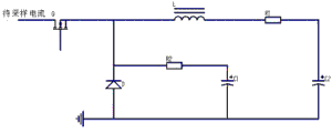
Fig. 1 is the circuit diagram of current sampling circuit in the utility model.
Embodiment
Below in conjunction with accompanying drawing, the utility model is done detailed explanation.
For the purpose, technical scheme and the advantage that make the utility model is clearer,, the utility model is further elaborated below in conjunction with accompanying drawing and embodiment.Should be appreciated that specific embodiment described herein only in order to explanation the utility model, and be not used in qualification the utility model.
As shown in Figure 1; This current sampling circuit is by filter coil, second resistance R 2, the first polar capacitor C1, the second polar capacitor C2, switching device Q and diode D; Wherein this filter coil is equivalent to the inductance L and first resistance R 1 of series connection; The free end of this inductance L connects the positive pole of the first polar capacitor C1 and the minus earth of this first polar capacitor C1 through second resistance R 2, and the free end of this first resistance R 1 connects the minus earth of anodal and this second polar capacitor C2 of the second polar capacitor C2; The free end of this inductance L connects the positive pole of diode D and the minus earth of diode D, and the free end of this inductance L is treated sample rate current through this switching device Q input.
U in this current sampling circuit
L+ I
L* R+U
2=U
1+ I
C1* R
', U wherein
L, I
LRepresent magnitude of voltage, current value on the inductance L respectively, R representes the resistance value of first resistance R 1, U
2Represent the magnitude of voltage on the second polar capacitor C2, U
1Represent the magnitude of voltage on the first polar capacitor C1, I
C1Represent the current value on first capacitor C 1, R
'The resistance value of representing second resistance R 2.The mean value that is pressed in the switch periods is 0 because inductance L powers on, i.e. U
L=0, and the mean value of first capacitor C 1 charging and discharging currents in a switch periods is 0, i.e. I
C1=0, then above-mentioned formula can be expressed as I
L* R+U
2=U
1, because the electric current I on the inductance L
LBe and treat sample rate current, therefore under the certain situation of the resistance value R of first resistance R 1, the magnitude of voltage that only need measure on first capacitor C 1 and second capacitor C 2 can obtain to treat sample rate current.The utility model converts current sample into voltage detecting, makes that this current sample method is simpler, lossless and cost is low.
In first embodiment of the utility model; This switching device Q selects the MOSFET pipe for use; The free end of this inductance L connects the source electrode of this MOSFET pipe, and the drain electrode of this MOSFET pipe is used for receiving treats that sample rate current and grid are used to receive control signal, realizes the conducting and the disconnection of MOSFET pipe.It should be noted: this switching device Q can also adopt IGBT pipe, pliotron and other device for power switching.
The above is merely the preferred embodiment of the utility model; Not in order to restriction the utility model; Any modification of being done within all spirit and principles at the utility model, be equal to replacement and improvement etc., all should be included within the protection domain of the utility model.
Claims (4)
1. current sampling circuit; It is characterized in that: comprise filter coil, second resistance (R2), first polar capacitor (C1) and second polar capacitor (C2); Wherein this filter coil is equivalent to the inductance (L) and first resistance (R1) of series connection; The free end of this inductance (L) is used for input to be treated sample rate current and passes through the positive pole that this second resistance (R2) connects first polar capacitor (C1), the minus earth of this first polar capacitor (C1); The free end of this first resistance (R1) connects the minus earth of anodal and this second polar capacitor (C2) of this second polar capacitor (C2).
2. current sampling circuit according to claim 1 is characterized in that: this current sampling circuit also comprises diode (D), and the free end of this inductance (L) connects the negative pole of diode (D) and the plus earth of this diode (D).
3. current sampling circuit according to claim 1 and 2 is characterized in that: this current sampling circuit also comprises switching device (Q), and wherein the free end of this inductance (L) is through this switching device (Q) input current.
4. current sampling circuit according to claim 3; It is characterized in that: said switching device (Q) is selected the MOSFET pipe for use; The free end of this inductance (L) connects the source electrode of MOSFET pipe; The drain electrode of MOSFET pipe is used for input and treats that sample rate current and grid are used to receive control signal, realizes that the conducting of MOSFET pipe is perhaps broken off.
Priority Applications (1)
| Application Number | Priority Date | Filing Date | Title |
|---|---|---|---|
| CN2012201384556U CN202494713U (en) | 2012-04-05 | 2012-04-05 | Current sampling circuit |
Applications Claiming Priority (1)
| Application Number | Priority Date | Filing Date | Title |
|---|---|---|---|
| CN2012201384556U CN202494713U (en) | 2012-04-05 | 2012-04-05 | Current sampling circuit |
Publications (1)
| Publication Number | Publication Date |
|---|---|
| CN202494713U true CN202494713U (en) | 2012-10-17 |
Family
ID=47000938
Family Applications (1)
| Application Number | Title | Priority Date | Filing Date |
|---|---|---|---|
| CN2012201384556U Expired - Fee Related CN202494713U (en) | 2012-04-05 | 2012-04-05 | Current sampling circuit |
Country Status (1)
| Country | Link |
|---|---|
| CN (1) | CN202494713U (en) |
-
2012
- 2012-04-05 CN CN2012201384556U patent/CN202494713U/en not_active Expired - Fee Related
Similar Documents
| Publication | Publication Date | Title |
|---|---|---|
| CN103018575B (en) | A kind of method utilizing large power, electrically sensing electricity testing device to measure high-power inductance | |
| CN110208597B (en) | A Self-Powered Wireless Current Monitoring System Based on Single Winding Current Transformer | |
| CN203840210U (en) | AC inverter circuit | |
| CN103872787B (en) | A kind of novel high-pressure side induction power taking supply unit | |
| CN113300487B (en) | Foreign matter detection device and method for wireless power transmission system | |
| CN205123588U (en) | It turns over to keep apart swashs formula high frequency switching power supply and input voltage detection circuitry thereof | |
| CN104242657A (en) | Non-contact resonant converter with primary side parallel and series connection compensation and secondary side series connection compensation | |
| CN102386780A (en) | Push-pull circuit of DC/DC (Direct Current/Direct Current) part | |
| CN208172223U (en) | A kind of stray transformer flux detection device | |
| CN203595790U (en) | Passive switch isolation detection apparatus | |
| CN202231621U (en) | Shunt-wound structure of current transformer | |
| CN202094711U (en) | Direct current supply device capable of obtaining electric energy from cable in service | |
| CN107733093A (en) | A kind of Capacitance Coupled resonance type wireless energy transmission system and method | |
| CN205103301U (en) | Hourglass current detection circuit who restraines common mode interference | |
| CN202494713U (en) | Current sampling circuit | |
| CN205017222U (en) | Switching power supply and electronic equipment | |
| CN102103157B (en) | Direct voltage isolated sampling device | |
| CN204361762U (en) | A kind of small rail car charging device based on electromagnetic induction | |
| CN208955659U (en) | A phase-controlled circuit breaker fundamental wave signal extraction device | |
| CN203166765U (en) | Isolation type DC/DC converter based on modularization multi-level transverter | |
| CN203434883U (en) | Self-excitation push-pull high-frequency converter | |
| CN110601379B (en) | A control method for realizing the electronic load function by using a single-phase AC/DC rectifier circuit applied to a current transformer | |
| CN206584812U (en) | A kind of optical fiber transferring high voltage current transformer of eccentrically arranged type | |
| CN203181262U (en) | High frequency electric welding bench electromagnetic induction heating system | |
| CN202256445U (en) | Voltage detection circuit |
Legal Events
| Date | Code | Title | Description |
|---|---|---|---|
| C14 | Grant of patent or utility model | ||
| GR01 | Patent grant | ||
| C17 | Cessation of patent right | ||
| CF01 | Termination of patent right due to non-payment of annual fee |
Granted publication date: 20121017 Termination date: 20140405 |