CN202026239U - High voltage starting switch and sensing field effect transistor (FET) multiplex circuit and switching power supply applying same - Google Patents
High voltage starting switch and sensing field effect transistor (FET) multiplex circuit and switching power supply applying same Download PDFInfo
- Publication number
- CN202026239U CN202026239U CN2011201285819U CN201120128581U CN202026239U CN 202026239 U CN202026239 U CN 202026239U CN 2011201285819 U CN2011201285819 U CN 2011201285819U CN 201120128581 U CN201120128581 U CN 201120128581U CN 202026239 U CN202026239 U CN 202026239U
- Authority
- CN
- China
- Prior art keywords
- resistance
- multiplex circuit
- power supply
- high voltage
- input
- Prior art date
- Legal status (The legal status is an assumption and is not a legal conclusion. Google has not performed a legal analysis and makes no representation as to the accuracy of the status listed.)
- Expired - Lifetime
Links
Images


Abstract
The utility model provides a high voltage starting switch and a sensing field effect transistor (FET) multiplex circuit, which can be applied to a switching power supply and the like. The multiplex circuit achieves starting through the high voltage starting switch and is capable of shutting the starting switch after starting to avoid damage to a starting circuit. Meanwhile, after starting the high voltage starting switch automatically serves as a sensing FET and achieves current-limiting and sensing functions of a main transformer of a switching mode power supply transformer. In addition, the utility model also provides a switching power supply applying the high voltage starting switch and the sensing FET multiplex circuit. The switching power supply is capable of well resolving the problem of loss to the starting circuit and reducing VS pin cost.
Description
Technical field
The utility model relates to a kind of high voltage startup switch and detects transistor
(SENSEFET) multiplex circuit and use the Switching Power Supply of this circuit.
Background technology
The switch power converter that is widely used on the consumer electronics product generally includes two kinds of forms: exchanging changes direct current (AC-DC) and DC-to-DC (DC-DC).Starter in the conventional switch mould power supply changeover device mostly is resistance.After power supply electrifying started, there was bigger power loss in starting resistance, and is bigger in underloading or holding state influence to power-efficient.In addition, conventional switch power supply changeover device switching current detects and all adopts external current-limiting resistance, has both increased power consumption and has also increased pin position cost.
For addressing the above problem, need provide new technology to finish Switching Power Supply startup and the detection of transformer primary current limliting.
Tradition startup method is mainly used resistance starting, and as shown in Figure 1, Fig. 1 has described a kind of power supply changeover device 10 based on traditional start-up technique.One control circuit, 20 lotus roots are connected to a back coupling unit 15, and to produce a switching signal VSW, this switching signal is regulated the output signal VO of power supply changeover device 10, and these back coupling unit 15 lotus roots are connected to the output of power supply changeover device 10, to produce a feedback signal VFB.Wherein this switching signal VSW changes according to feedback signal VFB.The switching current IS of one transformer TR1 is converted into voltage signal VS via picking up flow resistor RS.Switching signal VSW is accepted and produced in view of the above to this signal VS Be Controlled circuit 20.Switching signal VSW starts according to control circuit 20 inner UVLO circuit.Among the figure, control circuit 20 contains a UVLO circuit.This UVLO circuit lotus root is connected to VCC, according to VCC pin position voltage vcc in order to produce an internal circuit power supply signal VBIAS.VBAIS carries out operate as normal for inner other circuit provide power supply in order to start-up circuit 20.The VCC lotus root is connected to capacitor C in the pin position
VCC, in order to VCC pin position is powered.In addition, pin position VCC lotus root is connected to starting resistance R
ST, starting resistance R
STLotus root is connected to input power supply V
IN, in order to during initially powering on to capacitor C
VCCCharging.Between charge period, work as C
VCCAfter last current potential rose to a preset potential Vccon, UVLO circuit response VCC pin position produced VBIAS, and circuit 20 starts work fully, and start-up period finishes.To from above analysis, starting resistance R
STStill old electric current flows through after start-up period finishes, however conventional switch power initiation resistance R
STGenerally be about 1M Ω, then its maximum power dissipation is: P
ST0=380V
2/ 1M Ω=144mW.Therefore, traditional starter is very big to the light-load efficiency influence, is not easy by international efficiency standard (such as the star of american energy).In addition, the outside pin of Vs position has increased the IC cost.
Summary of the invention
In view of this, the purpose of this utility model provides a kind of high voltage startup switch and detects transistor (SenseFET) multiplex circuit, can be applicable to Switching Power Supply etc., finish by the high voltage startup switch and start and after startup, can close starting switch and avoid the start-up circuit loss.Simultaneously, start back high voltage startup switch and serve as SenseFET automatically, finish switching mode power supply transformer master margin current detection functionality.
High voltage startup switch of the present utility model and detection transistor multiplex circuit comprise switching signal (V
SW) input, starting current input (VST), switching current input (DRAIN), under-voltage locking input (UVLO), power supply input (VCC) and inspection stream end (V
S), it is characterized in that, also comprise: a power tube, its grid is connected with described switching signal input, and drain electrode is connected source ground with described switching current input; One injectron, its grid is connected with described starting current input, and drain electrode is connected with the drain electrode of described power tube; One first diode, its anode is connected with described switching signal input, and negative electrode is connected with the grid of described injectron; One the first transistor, its collector electrode is connected with the grid of described injectron through one first resistance, and base stage is connected grounded emitter through one second resistance with described under-voltage locking input; One clamped voltage-stabiliser tube, its plus earth, negative electrode is connected with the grid of described injectron; One galvanostat, it comprises: first output is connected with the grid of described injectron, and second output is connected with described power supply input through one second diode, and first input end is connected with described inspection stream end; And a transistor seconds, its collector electrode is connected through one the 3rd resistance and described inspection stream end, and base stage is connected grounded emitter through one the 4th resistance with described under-voltage locking input.
In the utility model one embodiment, described galvanostat is by one the 3rd transistor, one electric capacity, one the 5th resistance and the 6th resistance are formed, the described the 3rd transistorized collector electrode is connected with the grid of described injectron, the described the 3rd transistorized emitter, first end of described electric capacity and first end of the 6th resistance are connected with the anode of described second diode, the described the 3rd transistorized base stage is connected with second end of described electric capacity and first end of the 5th resistance, second end of described the 5th resistance is connected with described inspection stream end, and second end of described the 6th resistance is connected with described inspection stream end.
In the utility model one embodiment, described high voltage startup switch and detection transistor multiplex circuit are integrated in the integrated package.
Another purpose of the present utility model provides a kind of Switching Power Supply of using above-mentioned high voltage startup switch and SenseFET multiplex circuit, and this power supply can suppress start-up circuit loss problem preferably and save Vs pin position cost.
This purpose adopts following scheme to realize: a kind of Switching Power Supply of using above-mentioned high voltage startup switch and detecting the transistor multiplex circuit, it is characterized in that: comprise a transformer and a control circuit, it is characterized in that: described control circuit lotus root connects a back coupling unit of being located at the transformer output, and described control circuit comprises a described multiplex circuit and a PWM controller; First end of described primary is connected with the starting current input of described multiplex circuit through a resistance, and second end of described primary is connected with the switching current input of described multiplex circuit; The output lotus root of described PWM controller is connected to described multiplex circuit.
In the utility model one embodiment, described multiplex circuit and PWM controller are integrated in the integrated package.
The utility model adopts high voltage startup switch and SenseFET multiplex circuit to realize under the constant prerequisite of Switching Power Supply electrifying startup performance, reduce the loss of start-up circuit after the Switching Power Supply startup is finished greatly, can finish the detection of switching mode power supply transformer master margin stream simultaneously and not need to increase outside Vs pin position.This circuit can be designed to integrated circuit, and cost is low, has market value preferably.
Description of drawings
Fig. 1 is based on the power supply changeover device of conventional start-up circuit and the detection of transformer primary current limliting.
Fig. 2 is the utility model high voltage startup switch and the circuit connection diagram that detects the transistor multiplex circuit.
Fig. 3 is the high voltage startup switch of the utility model one embodiment and the circuit connection diagram that detects the transistor multiplex circuit.
Fig. 4 is based on the circuit theory schematic block diagram of the power supply changeover device of a kind of high voltage startup switch and SenseFET multiplex circuit.
The primary clustering symbol description:
SenseFET: detect transistor
20,300: control circuit
Q1, Q2, Q3, Q4: transistor
TR1: transformer
D1, D2, D3: diode
Z1: voltage-stabiliser tube
M1: injectron
M2: power tube
15,104: the back coupling unit
R
S, R
1, R
2, R
4, R
5, R
6, R
7, R
ST: resistor
C1, C2, C
VCC: capacitor
1000: a kind of high voltage startup switch and SenseFET multiplex circuit
The 2000:PWM controller
FB: feedback and hold
VCC: supply power voltage input
V
CC: supply power voltage
SW: switch output
V
FB: feedback voltage
V
IN: input voltage
V
O: output voltage
V
S: inspection stream voltage
I
S: switch current
I
VST: input current
U
In: input voltage
V
SW: switching signal.
Embodiment
Below in conjunction with drawings and Examples the utility model is described further.
As shown in Figure 2, the utility model provides a kind of high voltage startup switch and detects the transistor multiplex circuit, comprises switching signal V
SWInput, starting current input VST, switching current input DRAIN, under-voltage locking input UVLO, power supply input (VCC) and inspection stream end V
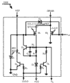
S, it is characterized in that, also comprise: a power tube M2, its grid is connected with described switching signal input, and drain electrode is connected source ground with described switching current input; One injectron M1, its grid is connected with described starting current input, and drain electrode is connected with the drain electrode of described power tube M2; One first diode D3, its anode is connected with described switching signal input, and negative electrode is connected with the grid of described injectron M1; One the first transistor Q3, its collector electrode is connected with the grid of described injectron M1 through one first resistance R 7, and base stage is through one second resistance R 4 and described under-voltage locking input, grounded emitter; One clamped voltage-stabiliser tube Z1, its plus earth, negative electrode is connected with the grid of described injectron M1; One galvanostat, it comprises: first output is connected with the grid of described injectron M1, and second output is connected with described power supply input through one second diode D2, and first input end is connected with described inspection stream end; And a transistor seconds Q4, its collector electrode is connected through one the 3rd resistance R 6 and described inspection stream end, and base stage is connected grounded emitter through one the 4th resistance R 5 with described under-voltage locking input.
Concrete, referring to Fig. 3, Fig. 3 is the circuit connection diagram of the high voltage startup switch and the SenseFET multiplex circuit of present embodiment, among the figure, the gate electrode lotus root of described transistor M1 is connected to the negative electrode of VST, Z1 and D3, the collector electrode of Q2, first end of R7, and the source electrode lotus root of this M1 is connected to second end and the V of R1, R2, R6
S, the drain electrode lotus root of this M1 is connected to the drain electrode of DRAIN and M2; The gate electrode lotus root of described M2 is connected to the anode of Vsw and D3, and the source electrode lotus root of this M2 is connected to earth potential; The base electrode lotus root of described Q2 is connected to second end of C2 and second end of R2, and the emission electrode lotus root of this Q2 is connected to first end and first end of R1 and the anode of D2 of C2; The base electrode lotus root of described Q3 is connected to first end of R4, and the emission electrode lotus root of this Q3 is connected to earth potential; The collector electrode lotus root of this Q3 is connected to second end of R7; The anode lotus root of described Z1 is connected to earth potential; The negative electrode lotus root of described D2 is connected to VCC; The second end lotus root of described R4 is connected to UVLO; Described UVLO lotus root is connected to first end of R5; The second end lotus root of described R5 is connected to the base electrode of Q4; The emitter lotus root of described Q4 is connected to earth potential; The collector electrode lotus root of described Q4 is connected to first end of R6.
High voltage startup switch described in the utility model and SenseFET multiplex circuit can be integrated in the integrated package, can reduce the volume and the cost of circuit greatly.
In order to allow those skilled in the art better understand the utility model, below our combined circuit operation principle of the present utility model is further described:
Please continue referring to Fig. 3, high voltage startup switch and SenseFET multiplex circuit 1000 be by transistor M1, power tube M2, and transistor Q2, Q3, Q4, diode D2, D3, voltage-stabiliser tube Z1, resistance R 1, R2, R4, R5, R6 and R7, and capacitor C2 forms.Power on when initial, VST is set in 26V, while UVLO=" 0 ", Q3 turn-offs, the M1 conducting is charged to the VCC port and is carried out start-up course, and after the VCC port voltage was elevated to predeterminated voltage VCCon, UVLO=" 1 " conducting Q3 was connected to earth potential with R7, the VST current potential will depend on Vsw, start to finish.Simultaneously, UVLO=" 1 " conducting Q4 is connected to earth potential with R6.2000 work of PWM controller produce pulse signal V
SW, M1 is according to V
SWCarry out switch motion.After powering on, because the VCC current potential is greater than VS, D2 ends so, the M1 electric current R6 that all flows through, and M1 serves as SenseFET automatically and detects the transformer primary current value.The detailed operation process is as follows:
During the electrifying startup, the VST port is set in 26V.R1, R2, Q2, C1 constitute galvanostat, and the channel current of M1 is carried out constant current control.
During the electrifying startup: when initial, VCC port current potential is 0.UVLO=" 0 ", V
SWBe earth potential, N type pipe Q3, Q4 turn-off, the gate electrode of high-voltage switch gear M1 by clamped at 26V, the M1 conducting, by galvanostat (constituting) and D2 by R1, R2, Q2, C1 to VCC port constant current charge to preset value VCCon, the UVLO upset is " 1 ", the Q3 conducting is conducting to R7 second end on the earth potential, Q4 conducting simultaneously is conducting to R6 second end on the earth potential, starts and finishes.2000 work of PWM controller produce pulse signal V
SW, M1 is according to V
SWCarry out switch motion, because D2 ends greater than the VS current potential because of the VCC current potential, the M1 electric current R6 that all flows through, M1 serves as SenseFET.Pulse signal V
SW, by the turn-on and turn-off of D3, R6, R7, Q3, Q4 Synchronization Control pipe M1, M2, therefore, M1 has produced mirror to M2, and the image current that the M1 pipe produces flows through resistor R 6 and produces inspection stream voltage signal V
SOutput to PWM controller 2000, finish detection switching mode power supply transformer master limit electric current.
Normal work period: after starting end, as long as VCC port current potential is higher than VCCmin, UVLO=" 1 ".D2 just ends, and does not have electric current, and whole starter circuit only has the VST port that electric current I is arranged
VSTFlow through (I
VST=V
IN/ Rst=V
IN/ 20M Ω≤19uA), so the power consumption estimation of starter normal work period is: P
ST=V
IN* I
VST≤ 380V*19uA=7.22mW(is Switching Power Supply input voltage V wherein
IN≤ 380V).So adopt the power supply changeover device start-up circuit maximum power dissipation of this circuit to be far smaller than the conventional power source transducer.(conventional power source transducer start-up circuit maximum power dissipation is 144mW).Also finish the built-in of switching mode power supply transformer master limit current detecting simultaneously, saved Sense pin position cost.
Be applied to by way of example in the power supply changeover device although be noted that the utility model here, the utility model itself has the wider range of application beyond the example.Can use other transistors also can reach equal effect such as Q2, Q3, Q4, D3, Z1 split into several electricity devices also can reach equal effect, and removal Q2, C2, R1, R2, R4 or the connection of change network wait and reach equal effect.
See also Fig. 4, Fig. 4 is based on the power supply changeover device 100 of high voltage startup switch and SenseFET multiplex circuit 1000, comprises a resistance R
ST(R
STGreater than 20M Ω), lotus root is connected on port V
INAnd between the VST, start power supply changeover device 100 in order to the VCC port of circuit 300 is charged by this resistance.The maximum current of this port VST is V
INmax/ R
ST=380V/20M Ω=19uA.One capacitor Cvcc lotus root is connected between port VCC and the earth potential, in order to circuit 300 is powered.
One control circuit, 300 lotus roots are connected to a back coupling unit 104, to produce a switching signal V
SW, this switching signal V
SWRegulate the output signal V of power supply changeover device
OThese back coupling unit 104 lotus roots are connected to the output V of power supply changeover device
O, to produce a feedback signal V
FBWherein, this switching signal V
SWBe according to feedback signal V
FBAnd change.
This control circuit 300 passes through the internal high pressure starting switch and SenseFET multiplex circuit 1000 reaches and the R of its cascade
STPower supply changeover device 100 is started.These circuit 1000 lotus roots are connected to circuit 2000 and VST port, and response UVLO signal carries out charge initiation via the capacitor Cvcc that port VST, 1000 pairs of VCC ports of circuit lotus root connect.These circuit 1000 lotus roots are connected to circuit 2000, DRAIN port.Port DRAIN response Vsw signal produces switching current Is, and this switching current Is circuit 1000 of flowing through produces voltage signal Vs.These circuit 2000 lotus roots are connected to circuit 1000, FB port, response signal V
FBProduce signal Vsw with Vs.These circuit 2000 lotus roots are connected to the VCC port, accept the power supply of VCC port, and produce control signal UVLO.Signal UVLO is input to circuit 1000.
Though the utility model discloses as above with preferred embodiment, yet it should not limit the utility model, any technical staff who is familiar with this field is not in breaking away from spirit and scope of the present utility model, when doing a little change and replacement.Therefore protection range of the present utility model is as the criterion when looking accompanying the claim person of defining.
Claims (5)
1. a high voltage startup switch and detect the transistor multiplex circuit comprises switching signal (V
SW) input, starting current input (VST), switching current input (DRAIN), under-voltage locking input (UVLO), power supply input (VCC) and inspection stream end (V
S), it is characterized in that, also comprise:
One power tube, its grid is connected with described switching signal input, and drain electrode is connected source ground with described switching current input;
One injectron, its grid is connected with described starting current input, and drain electrode is connected with the drain electrode of described power tube;
One first diode, its anode is connected with described switching signal input, and negative electrode is connected with the grid of described injectron;
One the first transistor, its collector electrode is connected with the grid of described injectron through one first resistance, and base stage is connected grounded emitter through one second resistance with described under-voltage locking input;
One clamped voltage-stabiliser tube, its plus earth, negative electrode is connected with the grid of described injectron;
One galvanostat, it comprises: first output is connected with the grid of described injectron, and second output is connected with described power supply input through one second diode, and first input end is connected with described inspection stream end;
And a transistor seconds, its collector electrode is connected through one the 3rd resistance and described inspection stream end, and base stage is connected grounded emitter through one the 4th resistance with described under-voltage locking input.
2. high voltage startup switch according to claim 1 and detection transistor multiplex circuit, it is characterized in that: described galvanostat is by one the 3rd transistor, one electric capacity, one the 5th resistance and the 6th resistance are formed, the described the 3rd transistorized collector electrode is connected with the grid of described injectron, the described the 3rd transistorized emitter, first end of described electric capacity and first end of the 6th resistance are connected with the anode of described second diode, the described the 3rd transistorized base stage is connected with second end of described electric capacity and first end of the 5th resistance, second end of described the 5th resistance is connected with described inspection stream end, and second end of described the 6th resistance is connected with described inspection stream end.
3. high voltage startup switch according to claim 1 and detection transistor multiplex circuit is characterized in that: described high voltage startup switch and detection transistor multiplex circuit are integrated in the integrated package.
4. an application rights requires 1 described high voltage startup switch and the Switching Power Supply that detects the transistor multiplex circuit, it is characterized in that: comprise a transformer and a control circuit, it is characterized in that: described control circuit lotus root connects a back coupling unit of being located at the transformer output, and described control circuit comprises a described multiplex circuit and a PWM controller; First end of described primary is connected with the starting current input of described multiplex circuit through a resistance, and second end of described primary is connected with the switching current input of described multiplex circuit; The output lotus root of described PWM controller is connected to described multiplex circuit.
5. the Switching Power Supply of high voltage startup switch according to claim 4 and detection transistor multiplex circuit, it is characterized in that: described multiplex circuit and PWM controller are integrated in the integrated package.
Priority Applications (1)
| Application Number | Priority Date | Filing Date | Title |
|---|---|---|---|
| CN2011201285819U CN202026239U (en) | 2011-04-27 | 2011-04-27 | High voltage starting switch and sensing field effect transistor (FET) multiplex circuit and switching power supply applying same |
Applications Claiming Priority (1)
| Application Number | Priority Date | Filing Date | Title |
|---|---|---|---|
| CN2011201285819U CN202026239U (en) | 2011-04-27 | 2011-04-27 | High voltage starting switch and sensing field effect transistor (FET) multiplex circuit and switching power supply applying same |
Publications (1)
| Publication Number | Publication Date |
|---|---|
| CN202026239U true CN202026239U (en) | 2011-11-02 |
Family
ID=44851173
Family Applications (1)
| Application Number | Title | Priority Date | Filing Date |
|---|---|---|---|
| CN2011201285819U Expired - Lifetime CN202026239U (en) | 2011-04-27 | 2011-04-27 | High voltage starting switch and sensing field effect transistor (FET) multiplex circuit and switching power supply applying same |
Country Status (1)
| Country | Link |
|---|---|
| CN (1) | CN202026239U (en) |
Cited By (3)
| Publication number | Priority date | Publication date | Assignee | Title |
|---|---|---|---|---|
| CN102185468A (en) * | 2011-04-27 | 2011-09-14 | 大连连顺电子有限公司 | Multiplexing circuit of high-voltage starting switch and SenseFET and switching power supply applying circuit |
| CN102710238A (en) * | 2012-05-29 | 2012-10-03 | 大连连顺电子有限公司 | Non-linear voltage-controlled oscillator with low temperature sensitivity and switching power source applying same |
| CN103378752A (en) * | 2012-04-25 | 2013-10-30 | 立锜科技股份有限公司 | Control circuit for voltage stabilizer and relevant control method |
-
2011
- 2011-04-27 CN CN2011201285819U patent/CN202026239U/en not_active Expired - Lifetime
Cited By (6)
| Publication number | Priority date | Publication date | Assignee | Title |
|---|---|---|---|---|
| CN102185468A (en) * | 2011-04-27 | 2011-09-14 | 大连连顺电子有限公司 | Multiplexing circuit of high-voltage starting switch and SenseFET and switching power supply applying circuit |
| CN102185468B (en) * | 2011-04-27 | 2013-05-01 | 大连连顺电子有限公司 | Multiplexing circuit of high-voltage starting switch and Sense FET and switching power supply applying circuit |
| CN103378752A (en) * | 2012-04-25 | 2013-10-30 | 立锜科技股份有限公司 | Control circuit for voltage stabilizer and relevant control method |
| CN103378752B (en) * | 2012-04-25 | 2016-01-06 | 立锜科技股份有限公司 | For control circuit and the relevant control method of pressurizer |
| CN102710238A (en) * | 2012-05-29 | 2012-10-03 | 大连连顺电子有限公司 | Non-linear voltage-controlled oscillator with low temperature sensitivity and switching power source applying same |
| CN102710238B (en) * | 2012-05-29 | 2014-12-17 | 大连连顺电子有限公司 | Non-linear voltage-controlled oscillator with low temperature sensitivity and switching power source applying same |
Similar Documents
| Publication | Publication Date | Title |
|---|---|---|
| CN102097928B (en) | High voltage starting circuit applied to AC/DC converter | |
| CN104124878B (en) | Power supply module, switching power source chip and switch power supply system | |
| CN203661377U (en) | Dual-winding single-stage primary side feedback type LED lamp drive circuit | |
| CN103887984A (en) | Isolating converter and switching power supply comprising same | |
| CN102185468B (en) | Multiplexing circuit of high-voltage starting switch and Sense FET and switching power supply applying circuit | |
| CN206595898U (en) | Secondary inverse-excitation type switch power-supply based on SP6650 | |
| CN109787482A (en) | Control chip and control method, constant pressure and flow device and isolation flyback PWM system | |
| CN109742839A (en) | A kind of charging control circuit and system of bootstrap capacitor | |
| CN103354690B (en) | Auxiliary-winding-free primary side controlled LED (light-emitting diode) driving circuit and PFC (power factor correction) constant-current control circuit thereof | |
| CN202026239U (en) | High voltage starting switch and sensing field effect transistor (FET) multiplex circuit and switching power supply applying same | |
| CN102437724B (en) | AC-DC (alternating current-direct current) chip, system and high-voltage startup control circuit of system | |
| CN202759634U (en) | LED drive circuit without auxiliary winding | |
| CN201928187U (en) | High-voltage start switch circuit and switch power applying high-voltage start switch circuit | |
| CN208094435U (en) | A kind of AC-DC Switching Power Supplies and its control chip | |
| CN203326888U (en) | Light-load and high-efficiency novel-type adapter power supply | |
| CN102170232B (en) | Self-driven active buffer and flyback switching mode power supply | |
| CN102832797A (en) | High-voltage current source multiplexing sampling circuit and switch power supply | |
| CN102931848B (en) | High-efficiency flyback power supply system applicable to liquid crystal display products | |
| CN202906730U (en) | Self-switching-on-off starting control circuit used for LED flyback driving power supply | |
| CN204014223U (en) | Low cost compact led drive circuit chip | |
| CN103683892B (en) | Switching Power Supply and controller thereof | |
| CN102064719B (en) | LED (Light Emitting Diode) backlight power source circuit, backlight power source and multimedia device | |
| CN206117538U (en) | Switching power supply circuit device that convergence was inputed in zero standby | |
| CN206135707U (en) | Utilize powerMOS pipe to realize AC of high -pressure quick start supply circuit for DC switching power supply | |
| CN202550872U (en) | AC-DC (alternating current-direct current) chip, system and high-voltage startup control circuit of system |
Legal Events
| Date | Code | Title | Description |
|---|---|---|---|
| C14 | Grant of patent or utility model | ||
| GR01 | Patent grant | ||
| AV01 | Patent right actively abandoned |
Granted publication date: 20111102 Effective date of abandoning: 20130501 |
|
| RGAV | Abandon patent right to avoid regrant |