CN201134974Y - Tri-dimensional circuit board - Google Patents
Tri-dimensional circuit board Download PDFInfo
- Publication number
- CN201134974Y CN201134974Y CNU2007201707833U CN200720170783U CN201134974Y CN 201134974 Y CN201134974 Y CN 201134974Y CN U2007201707833 U CNU2007201707833 U CN U2007201707833U CN 200720170783 U CN200720170783 U CN 200720170783U CN 201134974 Y CN201134974 Y CN 201134974Y
- Authority
- CN
- China
- Prior art keywords
- circuit board
- square groove
- metal pad
- plate
- substrate
- Prior art date
- Legal status (The legal status is an assumption and is not a legal conclusion. Google has not performed a legal analysis and makes no representation as to the accuracy of the status listed.)
- Expired - Fee Related
Links
Images


Abstract
The utility model relates to a vertical circuit board, which aims to solve the problems that a current flat type circuit board is difficult to be miniaturized, and the producing cost is high and the developing period is long when a multi-layer circuit board needs to be adopted as the circuits are complicated. The vertical circuit board provided by the utility model comprises at least one base plate and at least one board, wherein at least one square groove is arranged on the base plate, a metal welding disc is arranged on the square groove edges, the board is provided with at least one insert side, a metal pad which is corresponding to the metal pad on the square groove edges is arranged on the insert side, the insert side is inserted in the square groove, and the metal pad on the square groove edges and the metal pad on the insert side are welded to form the electric connection between the board and the base plate. The vertical circuit board can utilize the inner portions of electric appliances at a maximum degree, realizes the miniaturization of the circuit board, still can adopt a single-faced or a double-faced printing circuit when the circuits are complicated, avoids using a multi-layer printing circuit, shortens the developing period, and reduces the manufacture cost.
Description
Technical field
The utility model relates to a kind of circuit board, more particularly, relates to a kind of three-dimensional circuit board.
Background technology
Traditional printed circuit board (PCB) all is a planar structure, and in today that technical development is maked rapid progress, household electrical appliance are miniaturization more and more, wants miniaturization with regard to the inner used printed circuit board (PCB) of these electrical equipment of inevitable requirement.Under control complexity, inner space condition of limited, the printed circuit board (PCB) of plane often can't resolve problem.First, the plane printed circuit board (PCB) at most can only be at its tow sides welding electronic device, and double-edged area is limited, when handling complicated circuit, still circuit board must be done enough greatly holding more electronic component, so plane printed circuit board (PCB) miniaturization effectively sometimes; The second, because the circuit complexity, only the tow sides printed circuit at circuit board is not enough, must adopt multilayer circuit board, and the construction cycle of multilayer circuit board is long, production cost is high so that be unfavorable for product and participate in market competition.
The utility model content
The technical problems to be solved in the utility model is, big at existing plane printed circuit board sizes, can not effectively utilize the electrical equipment inner space etc. problem, can effectively utilize product inner space, low cost of manufacture, short three-dimensional circuit board of construction cycle and provide a kind of.
The technical scheme that its technical problem that solves the utility model adopts is: propose a kind of three-dimensional circuit board, comprise at least one substrate and at least one block of plate, described substrate is provided with at least one square groove, described square groove edge is provided with metal pad, described plate has at least one plug side, plug side is provided with and the corresponding metal pad of the metal pad at square groove edge, described plug side is inserted in the described square groove, and the metal pad at square groove edge welds the electric connection that forms between plate and the substrate mutually with metal pad on the plug side.
In three-dimensional circuit board described in the utility model, comprise a substrate and at least one block of plate, described plate has a plug side.
In three-dimensional circuit board described in the utility model, comprise two substrates and at least two blocks of plates, described two substrates is parallel to each other, and described plate two relative limits are two plug sides, described plate is between two substrates, and two plug sides on the plate are plugged on respectively in the square groove of two substrates.
In three-dimensional circuit board described in the utility model, the metal pad on the described plug side is arranged on a side of plug side, and the metal pad at described square groove edge also is arranged on a side of square groove accordingly; Metal pad on the described plug side also can be arranged on the both sides of plug side, and the metal pad at described square groove accordingly edge also is positioned at the both sides of square groove.
In three-dimensional circuit board described in the utility model, described plate is the single face circuit board, also can be double-sided PCB.
In three-dimensional circuit board described in the utility model, described substrate is the single face circuit board, also can be double-sided PCB.
In three-dimensional circuit board described in the utility model, the metal pad at described square groove edge is positioned at the front of substrate, also can be positioned at the reverse side of substrate.
Three-dimensional circuit board in the utility model is compared with existing plane circuit board, has following advantage:
1, circuit board is three-dimensional, can effectively utilize the solid space of electrical equipment, circuit board can dwindle circuit board under the prerequisite that maintains the area that enough is used to install electronic devices and components size.
2, the surface area that increases circuit board can adopt low-cost single face or double-sided printed-circuit board to make things convenient for the electronic devices and components line on the circuit board, avoids using expensive multilayer board, shortens the construction cycle and the manufacturing cost that reduces circuit board of circuit board.
Description of drawings
The utility model is described in further detail below in conjunction with drawings and Examples, in the accompanying drawing:
Fig. 1 is the structural representation of the three-dimensional circuit board among first embodiment of the utility model;
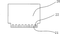
Fig. 2 is the structural representation of the substrate among first embodiment of the utility model;
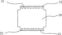
Fig. 3 is the structural representation of the plate among first embodiment of the utility model;
Fig. 4 is the structural representation of the three-dimensional circuit board among second embodiment of the utility model;
Fig. 5 is the structural representation of the substrate among second embodiment of the utility model;
Fig. 6 is the structural representation of the plate among second embodiment of the utility model.
Embodiment
Fig. 1 to Fig. 3 shows first embodiment of the present utility model.
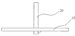
See also Fig. 1, Fig. 2 and shown in Figure 3, three-dimensional circuit board comprises a substrate 10 and a plate 20.Wherein substrate is provided with a square groove 11, and the width of square groove 11 is slightly greater than the thickness of plate 20, and the length of square groove 10 greater than the length of the plug side 21 of plate, is provided with metal pad 12 at the reverse side of substrate 10, a lateral edges of square groove 11 slightly.Plate 20 has a plug side 21, side at plug side all is provided with metal pad 21, the plug side 21 of plate is inserted in the square groove 11, this metal pad 21 is corresponding with the position of the metal pad 12 of square groove lateral margin, with scolder the corresponding metal pad on plate and the substrate 12,22 is welded, realize the electric connection of plate 20 and substrate 10, simultaneously plate is fixed on the substrate.
In the present embodiment, can offer many square grooves on substrate 10 according to the complexity of circuit, grafting polylith plate, substrate and plate also can be selected single-clad board or double-sided printed-circuit board for use as the case may be.
In the present embodiment, by grafting plate on substrate to form three-dimensional circuit board, make circuit board be used to install the size of dwindling circuit board under the situation of electronic element maintaining enough areas, make full use of the solid space of electronic product inside, simultaneously, because enough areas are arranged, circuit board can just adopt single or double form cheaply, and avoid adopting multilayer circuit board, to reach the purpose of construction cycle that shortens circuit board and the manufacturing cost that reduces circuit board.
Fig. 4 to Fig. 6 illustrates second embodiment of this utility model.
Present embodiment is compared with first embodiment, its difference is: the circuit board in the present embodiment has two substrates 10, two substrates 10 are parallel to each other, have two square grooves 11 on every block of plate, the two sides of square groove all are provided with metal pad 12, plate 20 also has two, two relative edges of every block of plate are two plug sides 21, the two sides of every plug side all are provided with metal pad 22, plate 20 is between two substrates 10, and two plug sides 21 of plate are plugged on respectively in the square groove 10 on the two substrates 10, by weld metal pad 12,22 realize the electric connection between plates and two substrates, simultaneously plate are fixedlyed connected with substrate.
In the present embodiment, can offer many square grooves respectively on two substrates 10 according to the complexity of circuit, grafting polylith plate, substrate and plate also can be selected for use as the case may be and be printed on one side or the circuit printing form of printed on both sides.
Claims (9)
1, a kind of three-dimensional circuit board, it is characterized in that: comprise at least one substrate and at least one block of plate, described substrate is provided with at least one square groove, described square groove edge is provided with metal pad, described plate has at least one plug side, plug side is provided with and the corresponding metal pad of the metal pad at square groove edge, and described plug side is inserted in the described square groove, and the metal pad at square groove edge welds the electric connection that forms between plate and the substrate mutually with metal pad on the plug side.
2, three-dimensional circuit board according to claim 1 is characterized in that: comprise a substrate and at least one block of plate, described plate has a plug side.
3, three-dimensional circuit board according to claim 1, it is characterized in that: comprise two substrates and at least two blocks of plates, described two substrates is parallel to each other, described plate two relative limits are two plug sides, described plate is between two substrates, and two plug sides on the plate are plugged on respectively in the square groove of two substrates.
4, according to any one described three-dimensional circuit board in claim 2 or 3, it is characterized in that: the metal pad on the described plug side is arranged on a side of plug side, and the metal pad at described square groove edge is positioned at a side of square groove.
5, according to any one described three-dimensional circuit board in claim 2 or 3, it is characterized in that: the metal pad on the described plug side is arranged on the both sides of plug side, and the metal pad at described square groove edge is positioned at the both sides of square groove.
6, according to any one described three-dimensional circuit board in claim 2 or 3, it is characterized in that: described plate is single face circuit board or double-sided PCB.
7, according to any one described three-dimensional circuit board in claim 2 or 3, it is characterized in that: described substrate is single face circuit board or double-sided PCB.
8, three-dimensional circuit board according to claim 7 is characterized in that: the metal pad at described square groove edge is positioned at the front of substrate.
9, three-dimensional circuit board according to claim 7 is characterized in that: the metal pad at described square groove edge is positioned at the reverse side of substrate.
Priority Applications (1)
| Application Number | Priority Date | Filing Date | Title |
|---|---|---|---|
| CNU2007201707833U CN201134974Y (en) | 2007-11-20 | 2007-11-20 | Tri-dimensional circuit board |
Applications Claiming Priority (1)
| Application Number | Priority Date | Filing Date | Title |
|---|---|---|---|
| CNU2007201707833U CN201134974Y (en) | 2007-11-20 | 2007-11-20 | Tri-dimensional circuit board |
Publications (1)
| Publication Number | Publication Date |
|---|---|
| CN201134974Y true CN201134974Y (en) | 2008-10-15 |
Family
ID=40063245
Family Applications (1)
| Application Number | Title | Priority Date | Filing Date |
|---|---|---|---|
| CNU2007201707833U Expired - Fee Related CN201134974Y (en) | 2007-11-20 | 2007-11-20 | Tri-dimensional circuit board |
Country Status (1)
| Country | Link |
|---|---|
| CN (1) | CN201134974Y (en) |
Cited By (5)
| Publication number | Priority date | Publication date | Assignee | Title |
|---|---|---|---|---|
| CN103687296A (en) * | 2013-12-20 | 2014-03-26 | 昌辉汽车电器(黄山)股份公司 | Circuit board assembly for car |
| CN105979703A (en) * | 2016-06-28 | 2016-09-28 | 广东欧珀移动通信有限公司 | PCB (Printed Circuit Board) assembly and mobile terminal with same |
| CN111656872A (en) * | 2018-01-31 | 2020-09-11 | 株式会社电装 | Electronic circuit |
| WO2021051225A1 (en) * | 2019-09-16 | 2021-03-25 | 深圳市雅信宏达电子科技有限公司 | Spliced circuit board |
| CN114535740A (en) * | 2022-03-03 | 2022-05-27 | 京信通信技术(广州)有限公司 | Antenna, radiation unit and welding method of radiation unit |
-
2007
- 2007-11-20 CN CNU2007201707833U patent/CN201134974Y/en not_active Expired - Fee Related
Cited By (8)
| Publication number | Priority date | Publication date | Assignee | Title |
|---|---|---|---|---|
| CN103687296A (en) * | 2013-12-20 | 2014-03-26 | 昌辉汽车电器(黄山)股份公司 | Circuit board assembly for car |
| CN103687296B (en) * | 2013-12-20 | 2016-07-06 | 昌辉汽车电器(黄山)股份公司 | A kind of circuit board assembly for car |
| CN105979703A (en) * | 2016-06-28 | 2016-09-28 | 广东欧珀移动通信有限公司 | PCB (Printed Circuit Board) assembly and mobile terminal with same |
| CN105979703B (en) * | 2016-06-28 | 2018-05-18 | 广东欧珀移动通信有限公司 | Pcb board component and with its mobile terminal |
| CN111656872A (en) * | 2018-01-31 | 2020-09-11 | 株式会社电装 | Electronic circuit |
| CN111656872B (en) * | 2018-01-31 | 2023-07-28 | 株式会社电装 | Electronic circuit |
| WO2021051225A1 (en) * | 2019-09-16 | 2021-03-25 | 深圳市雅信宏达电子科技有限公司 | Spliced circuit board |
| CN114535740A (en) * | 2022-03-03 | 2022-05-27 | 京信通信技术(广州)有限公司 | Antenna, radiation unit and welding method of radiation unit |
Similar Documents
| Publication | Publication Date | Title |
|---|---|---|
| CN201134974Y (en) | Tri-dimensional circuit board | |
| CN201093439Y (en) | LED heat sinking base plate | |
| CN202103944U (en) | Metal-base printed circuit board | |
| CN209545994U (en) | A kind of HDI PCB laminated construction | |
| CN215682799U (en) | Double-sided DIP wave soldering jig for double-sided SMT patch element | |
| CN201160130Y (en) | Electric connector assembly | |
| CN202488880U (en) | PCB (printed circuit board) capable of preventing hole from being plugged in tin soldering | |
| CN204836795U (en) | Grafting circuit board | |
| CN204634161U (en) | Segmented flexible circuit board | |
| CN201937023U (en) | Terminal block with terminal sheets in different shapes | |
| CN206282996U (en) | A kind of attachment structure of printed circuit board | |
| CN203760690U (en) | Switch mother end welding plug piece | |
| CN202050591U (en) | Double-sided filled aluminium base PCB board | |
| CN101146400A (en) | Printed circuit board assembly and its assembling method | |
| CN2922382Y (en) | Surface installation printed-circuit board circuit module | |
| CN203503933U (en) | Bidirectional interface on PCB | |
| CN204680854U (en) | Usb plug circuit board | |
| CN202308370U (en) | Improved structure of surface mount technology (SMT) type electric connector | |
| CN212163816U (en) | PCB circuit board that can multilayer be assembled | |
| CN218735136U (en) | Copper-clad plate | |
| CN209948084U (en) | Multifunctional wiring terminal | |
| CN204026552U (en) | Backboard, backlight module and display unit | |
| CN202772291U (en) | Electrical connector structure | |
| CN219181762U (en) | Multilayer PCB board for display screen | |
| CN219555416U (en) | Plug-in type multilayer circuit board |
Legal Events
| Date | Code | Title | Description |
|---|---|---|---|
| C14 | Grant of patent or utility model | ||
| GR01 | Patent grant | ||
| CF01 | Termination of patent right due to non-payment of annual fee | ||
| CF01 | Termination of patent right due to non-payment of annual fee |
Granted publication date: 20081015 Termination date: 20161120 |