CN1816841A - Electrophoretic display panel - Google Patents
Electrophoretic display panel Download PDFInfo
- Publication number
- CN1816841A CN1816841A CNA200480018922XA CN200480018922A CN1816841A CN 1816841 A CN1816841 A CN 1816841A CN A200480018922X A CNA200480018922X A CN A200480018922XA CN 200480018922 A CN200480018922 A CN 200480018922A CN 1816841 A CN1816841 A CN 1816841A
- Authority
- CN
- China
- Prior art keywords
- reset
- pel
- potential
- pulses
- drive unit
- Prior art date
- Legal status (The legal status is an assumption and is not a legal conclusion. Google has not performed a legal analysis and makes no representation as to the accuracy of the status listed.)
- Pending
Links
Images


Classifications
-
- G—PHYSICS
- G09—EDUCATION; CRYPTOGRAPHY; DISPLAY; ADVERTISING; SEALS
- G09G—ARRANGEMENTS OR CIRCUITS FOR CONTROL OF INDICATING DEVICES USING STATIC MEANS TO PRESENT VARIABLE INFORMATION
- G09G3/00—Control arrangements or circuits, of interest only in connection with visual indicators other than cathode-ray tubes
- G09G3/20—Control arrangements or circuits, of interest only in connection with visual indicators other than cathode-ray tubes for presentation of an assembly of a number of characters, e.g. a page, by composing the assembly by combination of individual elements arranged in a matrix no fixed position being assigned to or needed to be assigned to the individual characters or partial characters
- G09G3/34—Control arrangements or circuits, of interest only in connection with visual indicators other than cathode-ray tubes for presentation of an assembly of a number of characters, e.g. a page, by composing the assembly by combination of individual elements arranged in a matrix no fixed position being assigned to or needed to be assigned to the individual characters or partial characters by control of light from an independent source
- G09G3/3433—Control arrangements or circuits, of interest only in connection with visual indicators other than cathode-ray tubes for presentation of an assembly of a number of characters, e.g. a page, by composing the assembly by combination of individual elements arranged in a matrix no fixed position being assigned to or needed to be assigned to the individual characters or partial characters by control of light from an independent source using light modulating elements actuated by an electric field and being other than liquid crystal devices and electrochromic devices
- G09G3/344—Control arrangements or circuits, of interest only in connection with visual indicators other than cathode-ray tubes for presentation of an assembly of a number of characters, e.g. a page, by composing the assembly by combination of individual elements arranged in a matrix no fixed position being assigned to or needed to be assigned to the individual characters or partial characters by control of light from an independent source using light modulating elements actuated by an electric field and being other than liquid crystal devices and electrochromic devices based on particles moving in a fluid or in a gas, e.g. electrophoretic devices
-
- G—PHYSICS
- G09—EDUCATION; CRYPTOGRAPHY; DISPLAY; ADVERTISING; SEALS
- G09G—ARRANGEMENTS OR CIRCUITS FOR CONTROL OF INDICATING DEVICES USING STATIC MEANS TO PRESENT VARIABLE INFORMATION
- G09G2300/00—Aspects of the constitution of display devices
- G09G2300/08—Active matrix structure, i.e. with use of active elements, inclusive of non-linear two terminal elements, in the pixels together with light emitting or modulating elements
-
- G—PHYSICS
- G09—EDUCATION; CRYPTOGRAPHY; DISPLAY; ADVERTISING; SEALS
- G09G—ARRANGEMENTS OR CIRCUITS FOR CONTROL OF INDICATING DEVICES USING STATIC MEANS TO PRESENT VARIABLE INFORMATION
- G09G2310/00—Command of the display device
- G09G2310/06—Details of flat display driving waveforms
- G09G2310/061—Details of flat display driving waveforms for resetting or blanking
-
- G—PHYSICS
- G09—EDUCATION; CRYPTOGRAPHY; DISPLAY; ADVERTISING; SEALS
- G09G—ARRANGEMENTS OR CIRCUITS FOR CONTROL OF INDICATING DEVICES USING STATIC MEANS TO PRESENT VARIABLE INFORMATION
- G09G2310/00—Command of the display device
- G09G2310/06—Details of flat display driving waveforms
- G09G2310/065—Waveforms comprising zero voltage phase or pause
Landscapes
- Engineering & Computer Science (AREA)
- Physics & Mathematics (AREA)
- Computer Hardware Design (AREA)
- General Physics & Mathematics (AREA)
- Theoretical Computer Science (AREA)
- Control Of Indicators Other Than Cathode Ray Tubes (AREA)
Abstract
An electrophoretic display panel (1), comprises drive means (100), for controlling the potential difference of each picture element (2) to be a reset potential difference having a reset value and a reset duration for enabling particles (6) to substantially occupy one of the extreme positions. The reset pulses are applied in two or more pulses separated by a non-zero time interval during a reset period (Preset).
Description
Technical field
The present invention relates to a kind of electrophoretic display panel, comprising:
-one electrophoretic medium that comprises charged particle;
-a plurality of pels;
-being associated with each pel is used to receive the electrode of a potential difference (PD); With
-drive unit,
Each the potential difference (PD) that this drive unit is arranged for controlling in these a plurality of pels is:
-one has reset values and the reset potential of duration that resets, and is subsequently during the reset cycle
-one gray shade scale potential difference (PD) makes particle can occupy the position corresponding to image information.
The present invention also relates to a kind of method that is used to drive electro phoretic display device, in the method, before applying gray-scale data, reset pulse is applied to each unit of display device.
The invention still further relates to a kind of drive unit that is used to drive this electrophoretic display panel.
Background technology
An embodiment of the electrophoretic display panel of the sort of type of mentioning in the opening paragraph is described in International Patent Application WO 02/073304.
In described electrophoretic display panel, during picture showed, each pel had by the determined outward appearance of particle position.But particle position not only depends on potential difference (PD), and depends on the history of potential difference (PD).As the result who applies reset potential, the outward appearance of pel reduces the dependence of history, because particle occupies an extreme position (extreme position) substantially before applying the gray shade scale potential difference (PD).Thereby pel resets to one of ultimate limit state at every turn.Subsequently, as the result of picture potential difference (PD), particle occupies this position to show the gray shade scale corresponding to image information." gray shade scale " is appreciated that to meaning any intermediateness.When demonstration was white and black displays, " gray shade scale " was in fact relevant with the gradient of gray scale, and when using the colour cell of other types, " gray shade scale " is appreciated that to comprising any intermediateness between the ultimate limit state.
When image information changed, pel resetted.The inventor recognizes that during resetting voltage applies the image on the display may demonstrate irregular variation in this image, and this is unappealing for the beholder.Particularly the transformation from an image to another image may be irregular in the extreme.
Summary of the invention
An object of the present invention is to provide the sort of display screen of mentioning in the opening paragraph, it can provide the more level and smooth transformation from an image to another image.
This purpose is achieved in that drive unit also is arranged for being used for pel is reset to an extreme optical state from an optical states during the reset cycle, apply reset potential in two that are separated by the non-zero time interval and more pulse.
Pel is reset to one of ultimate limit state need apply reset potential different pels.The total duration that applies reset potential preferably becomes this optical states, and (it can be an intermediate optical state before resetting, i.e. gray shade scale) and the function of the difference between pel this extreme optical state that will reset to, promptly when a pel for white must reset to black state, promptly reset to an extreme optical state from an extreme optical state, be during a long relatively time cycle, to apply reset potential, if and pel will be from the dark-grey black state that resets to, promptly reset to an extreme optical state from an intermediate optical state, then reset potential only need apply and reach a relatively short time cycle.Thereby to a reset potential existence maximum application time (cycle reset time).As what the inventor recognized, in a pulse to applying a reset potential from each unit that for example optical states of a middle gray grade resets to an extreme position (for example from a gray-scale value to black state), yo-yo effect (shock effect) in the time of will causing from an image to another image transformation, especially under the significantly different situation of image, this yo-yo effect is unappealing for the beholder.This reset potential missionary society of distribution causes the more level and smooth conversion from an image to next image in the two or more pulses that separated by a non-zero time interval.
Preferably, drive unit is arranged to be used at reset cycle (P
Reset) during in two or more pulses, apply reset potential so that a pel is reset to an extreme optical state from an optical states, thereby the general reset current potential application time that all images conversion is had is shorter and longer than minimum value than maximal value.
In notion of the present invention, still can a short pulse or a very long pulse, apply from a grey level transition that is equivalent to or is in close proximity to ultimate limit state, as long as at least one intermediate optical state, and the conversion of preferably most intermediate optical state to an extreme optical state uses the two or more pulses that separated by the non-zero time interval to get final product.Preferably two or more pulses are used in all conversions with total application time longer and shorter than upper threshold value than lower threshold value.The constraint that applies cycle regular time that often is subjected to (for example frame time) of reset pulse, wherein the reset cycle be fixed time period integer (for example N) doubly.Need the conversion (0,1 of fixed time period maybe may be 2 times) of very short overall pulse not carry out in the pulse of partition, as may being the long pulse to the N of this fixed time period of needs or N-1 conversion doubly at one.
Two or more pulses preferably have identical polarity.
In an embodiment, reset potential is distributed in more than in two pulses for some conversions at least.That this has caused yo-yo effect even further reduce.
Reset potential distributes in two pulses in an embodiment.Such scheme needs minimum energy.
Preferably drive unit is arranged in two or more pulses and applies reset potential, and wherein to the conversion from least one intermediate optical state to one ultimate limit state, applied pulse has the duration of equal time basically.
This pulse has equal lengths basically, thereby causes level and smooth relatively image transitions.
Preferably drive unit is arranged for applying reset potential in two or more pulses, wherein for the conversion of at least one intermediate optical state to one extreme optical state, pulse was separated by at least two non-zero time intervals, and there is equal lengths basically in the time interval.
Make the time interval between the pulse, especially have under the situation of equal length, have identical length and can cause a very level and smooth image transitions in pulse itself.
When drive unit can be controlled reset pulse, make at least some conversions to be applied when resetting (overreset) advantageous particularly of the present invention.
And, if it was a sequence of preset potential differences before becoming reset potential that drive unit can also be controlled this potential difference (PD) for each pel, then be very favorable, this sequence of preset potential differences has prevalue and presetting the duration of being associated, prevalue symbol in this sequence alternately, each preset potential difference is represented a preset energy, this energy is enough to the particle that exists in will one of described extreme position and discharges from their position, but not enough so that described particle can reach another extreme position.As an advantage, sequence of preset potential differences has reduced the dependence of pel outward appearance to potential difference (PD) history.
According to the present invention, a kind of method that is used to drive electro phoretic display device is provided, comprising:
-one electrophoretic medium that comprises charged particle;
-a plurality of pels, in the method, before applying gray-scale data, the unit that reset pulse is applied to display device is used to the pel that resets, and it is characterized in that (P during the reset cycle
Reset), in the two or more pulses that separate by the non-zero time interval, apply reset potential, be used for pel is reset to an extreme optical state from an optical states.
And, according to the present invention, being provided for driving the drive unit of an electrophoretic display panel, described display screen comprises:
-one electrophoretic medium that comprises charged particle;
-a plurality of pels; With
-being associated with each pel is used to receive the electrode of potential difference (PD);
The potential difference (PD) that described drive unit is arranged for controlling each pel is
-have reset values and the reset potential of the duration that resets, be used to make particle can occupy one of extreme position substantially, and be subsequently
-picture potential difference (PD) is used to make particle (6) can occupy position corresponding to image information,
Described drive unit further is arranged to and is used for (P during the reset cycle
Reset), in the two or more pulses that separate by the non-zero time interval, apply reset potential, be used for pel is reset to an extreme optical state from an optical states.
Description of drawings
With reference to accompanying drawing, these and other aspects of display screen of the present invention will further be illustrated and describe, wherein:
Fig. 1 has schematically shown the front elevation of the embodiment of display screen;
Fig. 2 has schematically shown the cross-sectional view of the II-II in Fig. 1;
Fig. 3 has schematically shown the xsect of a part of another example of electro phoretic display device;
Fig. 4 has schematically shown the equivalent electrical circuit of the picture display device of Fig. 3;
Fig. 5 A schematically is shown as potential difference (PD) the function of time of the pel of the subclass that is used for embodiment;
Fig. 5 B schematically is shown as potential difference (PD) the function of time of the pel of the subclass that is used for the embodiment distortion;
Fig. 6 A schematically is shown as potential difference (PD) the function of time of the pel of the subclass that is used for another distortion of embodiment;
Fig. 6 B schematically is shown as potential difference (PD) and is used for the be associated function of time of another pel of subclass of identical distortion of embodiment with Fig. 5 A;
Fig. 7 show in another distortion of representing embodiment, as the average picture of the result's of reset potential first and second outward appearances and
Fig. 8 show in another distortion of representing embodiment, as the average picture of the result's of reset potential first and second outward appearances.
Fig. 9 schematically is shown as potential difference (PD) the function of time of the pel of the subclass that is used for another distortion of embodiment.
Figure 10 A and 10B represent according to embodiments of the invention, do not have reset pulse partition (Figure 10 A) and have the break scheme of (Figure 10 B) of reset pulse.
Figure 11 A and 11B represent according to embodiments of the invention, do not have reset pulse partition (Figure 11 A) and have the break another program of (Figure 11 B) of reset pulse.
Figure 12,13,14A, 14B and 15 show another example of the scheme of reset pulse partition.
Figure 16 is up to the various schemes of the complicacy of 23 expression increase reset pulses, and Figure 16 and 17 shows the scheme outside the scope of the invention, and Figure 18 is up to 23 schemes that show within the scope of the invention.
Figure 24 represents good effect of the present invention.
In all figure, corresponding part is quoted with identical Reference numeral usually.
Embodiment
Fig. 1 and 2 shows the embodiment of a display screen 1, and display screen has first substrate 8, the second relative substrate 9 and a plurality of pel 2.Pel 2 is preferably arranged along straight basically line in two-dimensional structure.Alternatively other arrangements of pel 2 also are possible, for example honeycomb arrangement.Electrophoretic medium 5 with charged particle 6 is present between the substrate 8,9.First and second electrodes 3,4 are associated with each pel 2.Electrode 3,4 can receive a potential difference (PD).Among Fig. 2, first substrate 8 has first electrode 3 to each pel 2, and second substrate 9 has second electrode 4 to each pel 2.Charged particle 6 can occupy near the extreme position of electrode 3,4 and the centre position between the electrode 3,4.Each pel 2 has by the determined outward appearance in the position of the charged particle between the electrode 3,46, so that show this picture.Electrophoretic medium 5 itself is from for example US5, and 961,804, US6,120,839 and US6,130,774 is known and can for example obtain from E Ink Corporation.As example, electrophoretic medium 5 is included in the electronegative black particles 6 in the white fluid.When as potential difference (PD) being 15 volts result for example, charged particle 6 is at first extreme position, and during promptly near first electrode 3, the outward appearance of pel 2 for example is white.Here think that pel 2 is from second substrate, 9 unilateral observations.When being opposite polarity as potential difference (PD), volt result promptly-15, charged particle 6 is at second extreme position, and during promptly near second electrode 4, the outward appearance of pel 2 is a black.When charged particle 6 centre position therein, promptly between the electrode 3,4 time, pel 2 has an outward appearance placed in the middle, for example, light gray, middle ash and dark-grey, they are the gray shade scales between white and the black.The potential difference (PD) that drive unit 100 is arranged for controlling each pel 2 is a reset potential, it has a reset values and a duration that resets, be used to make particle 6 can occupy one of them extreme position basically, and this potential difference (PD) is one subsequently and make particle 6 can occupy the picture potential difference (PD) corresponding to the position of this image information.
Fig. 3 has schematically shown the xsect of a part of another example of electro phoretic display device 31, this part for example has several display unit sizes, comprise a base substrate 32, an electrocoating film that has electric ink, it is present in two for example poly transparent substrates 33, between 34, one of substrate 33 provides transparent picture electrode 35, and another substrate 34 provides transparent counter electrode 36.Electric ink comprises a plurality of about 10 to 50 microns microcapsules 37.Each microcapsules 37 comprises white particles 38 and the electronegative black particles 39 that is suspended in the positively charged in the fluid F.When positive electric field was applied to pixel electrode 35, as seen a side and display unit that white particles 38 moves to the sensing counter electrode 36 of microcapsules 37 became the beholder.Simultaneously, black particles 39 moves to the opposite side of microcapsules 37, there the beholder is hidden them.By pixel electrode 35 is applied negative electric field, black particles 39 moves to a side of the sensing counter electrode 36 of microcapsules 37, and display unit is to the blackening of beholder's (not shown).When removing electric field, particle 38,39 remains on resulting state, and display represents bi-stable character and consumed energy not basically.
Fig. 4 has schematically shown the equivalent electrical circuit of a picture display device 31, comprises the electrocoating film, line driver 46 and the row driver 40 that are layered on the base substrate 32 that is equipped with active converting unit.Preferably counter electrode 36 is provided on the film of the electrophoretic ink that comprises encapsulation, but alternatively also can be provided on the base substrate under the situation of using the plane electric fields operation.Display device 31 is a thin film transistor (TFT) 49 by the active switch unit drives in this example.It is expert at or selects and comprises a matrix of display elements on the intersection region of electrode 47 and row or data electrode 41.Line driver 46 is selected column electrode 47 continuously, and row driver 40 provides a data-signal to row electrode 41 simultaneously.Best, processor 45 at first is treated to data-signal with the data 43 that enter.Realizing through driver circuit 42 synchronously mutually between row driver 40 and the line driver 46.Selection signal from line driver 46 is selected pixel electrode 42 through thin film transistor (TFT) 49, and the gate electrode 50 of thin film transistor (TFT) is electrically connected to column electrode 47, and source electrode 51 is electrically connected to row electrode 41.The data-signal that exists on row electrode 41 is sent to the pixel electrode 52 of display unit, and this display unit is coupled to drain electrode through TFT.In an embodiment, the display device of Fig. 3 also comprises a building-out condenser 53 that is in the position of each display unit 48.In this embodiment, building-out condenser 53 is connected to one or more storage capacitor lines 54.Replace TFT, also can use other switch elements, such as diode, MIM etc.
As an example, before applying reset potential, the outward appearance of the pel of a subclass is a light gray, is expressed as G2.And, be dark-grey corresponding to the picture outward appearance of the image information of this identical pel, be expressed as G1.Example hereto, the potential difference (PD) of pel is shown as the function of time in Fig. 5 A.Reset potential for example has 15 volts value and from time t
1To time t '
2There is t
2Be the maximum reset duration, i.e. reset cycle P
ResetReset duration and maximum reset duration for example is respectively 50ms and 300ms.As a result, pel has the outward appearance of white basically, represents with W.The picture potential difference (PD) is from time t
3To time t
4Value that exists and for example-15 have volt and the duration of for example 150ms.As a result, the outward appearance that pel has dark-grey (G1) is so that show this picture.From time t
2To time t
3The interval can not have.
To the maximum reset duration of each pel of this subclass, promptly the complete reset cycle is substantially equal to or changes to from an extreme position greater than the position with the particle 6 of each pel the duration of another extreme position.For the pel in this example, with reference to the duration for example be 300ms.
As another example, the potential difference (PD) of pel is shown as the function of time in Fig. 5 B.Before applying reset potential, the outward appearance of pel is dark-grey (G1).And, be light gray (G2) corresponding to the picture outward appearance of the image information of pel.Reset potential has for example 15 volts value, and from time t
1To time t '
2Exist.Duration that resets for example is 150ms.As a result, pel has the outward appearance of white (W) basically.The picture potential difference (PD) is from time t
3To time t
4Exist and for example have-value of 15V and the duration of for example 50ms.As a result, pel has the outward appearance of light gray (G2), so that show this picture.
In the distortion of the another kind of embodiment, drive unit 100 also is arranged to control the reset potential of each pel, makes particle 6 can occupy the extreme position of the position of the most approaching particle 6 corresponding to image information.As an example, before applying reset potential, the outward appearance of pel is light gray (G2).And, be dark-grey (G1) corresponding to the picture outward appearance of the image information of this pel.For this example, the potential difference (PD) of pel is expressed as the function of time in Fig. 6 A.Reset potential for example has-15 volts value and from time t
1To time t '
2Exist.Duration that resets for example is 150ms.As a result, particle 6 occupies second extreme position and pel has the outward appearance of black basically, represent with B, and the position of its most approaching particle 6 corresponding to image information, promptly pel 2 has dark-grey outward appearance (G1).The picture potential difference (PD) exists from time t3 to time t4, and has for example, for example the duration of 15 volts value and for example 50ms.As a result, pel 2 has the outward appearance of dark-grey (G1), so that show this picture.As another example, before applying reset potential, the outward appearance of another pel is light gray (G2).And, be white (W) basically corresponding to the picture outward appearance of the image information of this pel.For this example, the potential difference (PD) of pel is shown as the function of time in Fig. 6 B.Reset potential for example has 15 volts value and from time t
1To time t '
2Exist.Duration that resets for example is 50ms.As a result, particle 6 occupies first extreme position and pel and has the outward appearance (W) of white basically, the position of its most approaching particle 6 corresponding to image information, and promptly pel 2 has the outward appearance of white basically.Because outward appearance has been white basically, so the picture potential difference (PD) is from time t
3To time t
4Exist, and have for example 0 volt value, so that show this picture.
In Fig. 7, pel is arranged along straight basically line 70.If particle 6 occupies one of them extreme position basically, first extreme position for example, then pel has the first equal basically outward appearance, for example white.If particle 6 occupies another extreme position basically, second extreme position for example, then pel has the second equal basically outward appearance, for example black.Drive unit also is arranged for controlling the reset potential along the follow-up pel 2 of every line 70, makes particle 6 occupy dispar extreme position basically.Fig. 7 shows the average picture of representative as the result's of reset potential first and second outward appearances.Ash during this picture is represented basically.
In the distortion of this equipment, the potential difference (PD) that drive unit also is arranged for controlling each pel was a sequence of preset potential differences before becoming reset potential.Best, sequence of preset potential differences has prevalue and presetting the duration of being associated, prevalue symbol in the sequence alternately, each preset potential difference is represented a preset energy, and the particle 6 that this energy is enough to be present in one of them extreme position discharges from their position but be not enough so that described particle 6 can arrive another extreme position.As an example, before applying sequence of preset potential differences, the outward appearance of pel is a light gray.And, be dark-grey corresponding to the picture outward appearance of the image information of pel.Example hereto, the potential difference (PD) of pel is expressed as the function of time in Fig. 9.In this example, the sequence of preset potential difference has from time t
0To time t '
0Four prevalues that apply are followed successively by 15 volts, and-15 volts, 15 volts and-15 volts.Each prevalue applies and reaches for example 20ms.T '
0And t
1Between the time interval preferably relatively little.Subsequently, reset potential has-15 volts value and from time t
1To time t '
2Exist.Duration that resets for example is 150ms.As a result, particle 6 occupies second extreme position and pel has the outward appearance of black basically.The picture potential difference (PD) is from time t
3To time t
4Exist also to have for example, duration of 15 volts value and for example 50ms for example, the result, pel 2 has dark-grey outward appearance so that show this picture.Be not subjected to the specific explanations of the mechanism of the good effect of support applications presetting pulse is retrained, suppose that the application of presetting pulse has increased the momentum of electrophoresis particle, thereby and shortened switching time, promptly realize conversion, just the required time of appearance change.Also might switch to a predetermined state at display device, for example behind the black state, electrophoresis particle " is freezed " by the gegenion around the particle.Switching when subsequently is during to white states, and these gegenions must be discharged in time, and this needs the extra time.The release of gegenion has been quickened in the application of presetting pulse, thereby has quickened thawing of electrophoresis particle, has therefore shortened switching time.
Figure that the front is all and explanation relate to the General Principle that applies reset pulse, may additionally use presetting pulse.
As explained above, the precision of the gray shade scale in the electrophoresis showed is subjected to the influence of side inhomogeneity of image history, the residence time, temperature, humidity, electrophoretic foil etc. to a great extent.Use reset pulse, can realize accurate gray level, because gray level always realizes from reference black (B) or from reference white color state (W) (two ultimate limit states).Pulse train is partly formed by two or four usually: shake pulse (shaking pulse) (selectively, after this being also referred to as shake 1), reset pulse, shake pulse (selectively, after this being also referred to as shake 2) and gray shade scale driving pulse.The shortcoming of this method is to introduce at establishment intermediate image (reset mode) with gray level to have very long time delay between the demonstration, promptly postpones t '
2-t
3, particularly for the needs pixel of short image update sequence, for example for state exchange to a ultimate limit state from approaching a ultimate limit state, for example, from light gray to white or from dark-grey to black.This postpones, and perhaps the difference on the effective time delay between the different units can cause gray level stiff introducing visually more specifically, and is that the beholder is visible.
An object of the present invention is to provide the sort of display screen of mentioning in the opening paragraph, it can provide the more level and smooth transformation from an image to another image.
This purpose realizes that therefrom that is: drive unit also is arranged at reset cycle (P
Reset) during, in the two or more pulses that separate by time cycle, apply reset potential so that with a pel from one for example the middle gray grade (G1, optical states G2) reset to an extreme position (B, W).Best, these pulses have identical polarity.
In according to equipment of the present invention, drive unit is arranged for driving the scheme with at least two bit gradation grades, wherein particularly in short relatively image update sequence, at least some reset pulses are broken in two short pulses that separated by a time interval at least.These short reset pulses that broken are filled in the required time cycle (P of reset pulse in the long image update sequence more equably
Reset), cause image change progressively.By this way, the delay between the interpolation that resets to black/white image and gray shade scale is minimized, and has obtained more natural/level and smooth picture appearance.Total image update time remains basically unchanged.
Also used the shake pulse in a preferred embodiment.
The present invention also will demonstrate with further reference to several embodiment.
Embodiment 1
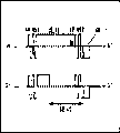
Embodiments of the invention 1 schematically show in Figure 10 B, and Figure 10 A shows not according to drive scheme of the present invention.In this example, show to have 2-bit gradation level at least: black (B), dark-grey (G1), light gray (G2) and white (W), realize respectively two conversions from W and G1 to the G1 state, long sequence is used for the conversion from W to G1, and this weak point sequence is used for the conversion from G1 to G1.Each sequence is made up of four parts among Figure 10 A and the 10B: shake 1 resets shake 2 and driving.Now, the single reset pulse of (G1 is to G1) is divided into six short reset pulses that are used for Figure 10 B in the short sequence of Figure 10 A, their reset pulses in long conversion sequence (W is to G1) equal in length and with equal range distribution in required time cycle, promptly separate, and the single reset pulse in the long sequence remains unchanged by the time interval that equates.In this example, in order to simplify, the burst length summation in these short pulses is taken as with the pulse width of original single reset pulse and equates.Because ink, might depart from the pulse width (longer than it usually) of single reset pulse in the summation in the burst length in these short pulses in response to the nonlinear characteristic of voltage impulse, thereby reaches the clearly reset optical state of definition.Delay between the interpolation of black state and the gray shade scale of resetting is minimized and obtains more natural picture appearance now under the situation that does not increase total image update time.The partition of pulse and the distribution on the reset cycle alleviates or the yo-yo effect that reduced at least to mention.
In this scheme, the conversion from G2 (light gray) to G1 (dark-grey) can be by not using reset pulse, and the reset pulse of the length between two parties of length shown in applying relatively respectively (promptly longer than the conversion from G1 to B, but shorter than the conversion from W to B) is realized.Reset pulse G2-B will be divided into for example 8 or 9 short pulses or 2 to 3 long relatively pulses like this.
Perhaps drive scheme can obtain simplifying by using the notion that resets, and was about to the unit ultimate limit state of intentionally overdriving.
This is at Figure 11 A, shown in the 11B, in virgin state is under the situation of G2 (light gray) and B (black), resetted when showing using, four kinds from W, G2, G1, B uses two types pulse train to realize to the conversion of G1 state: being used for from G2 or W (is identical length for G2 and W promptly to the long sequence of G1 conversion, this means that to G2 applying a mistake resets) and be used for G1 or B to the short sequence of G1 (this means that to B applying a mistake resets because strictly speaking black virgin state do not need to apply a reset pulse and to a black state).Each sequence is made up of four parts: shake 1 resets shake 2 and driving.Single reset pulse (G1/B is to G1) in the now short sequence is divided into six short reset pulses, their reset pulses in long conversion sequence are the range distribution (G2/W is to G1) to equate in required time cycle, and the single reset pulse of growing in the sequence remains unchanged.
Embodiments of the invention 2 schematically show in Figure 12, six short reset pulses that wherein have an equal pulse width are in long conversion sequence, in reset pulse range distribution (G2/W is to G1) not wait in the required time cycle, and the single reset pulse of growing in the sequence remains unchanged.
Embodiments of the invention 3 schematically show in Figure 13, wherein be used for G1 or B and be divided into four short reset pulses with unequal impulse width to the reset pulse of the short sequence of G1 conversion, they are in long conversion sequence, in reset pulse range distribution (G2/W is to G1) not wait in the required time cycle, and the single reset pulse of growing in the sequence remains unchanged.
Embodiments of the invention 4 schematically show in Figure 14 B, and wherein the length of the reset pulse that uses in various sequences is directly proportional in the distance that vertical direction need move with ink.For relatively, not according to original waveform of the present invention also shown in Figure 14 A.For example, in the driving of width modulation, in order to show that resetting to black from white needs overall pulse width (FPW), and from G2 reset to black only need FPW 2/3 and reset to black from G1 and only need 1/3 of FPW.Do not apply the shake pulse.These waveforms are available when the driving method that for example uses based on transition matrix, wherein consider previous image when determining impulse (time * voltage) for next image.And the ink material that uses in showing may use these waveforms to the history of image and/or the residence time when insensitive.Have again, from G2, G1 and B are divided into the several short reset pulse (Figure 14 B) with the pulse width that does not wait to the single reset pulse (Figure 14 A) in the short sequence of G1, their reset pulses in long conversion sequence (W is to G1) are the range distribution not wait in required time cycle, and single reset pulse remains unchanged in the sequence and grow.In order to simplify, the summation in burst length is taken as once more and equals the original single pulse width that resets in these short pulses.Delay between the interpolation of black state and the gray shade scale of resetting is minimized and obtains more natural picture appearance now under the situation that does not increase total image update time.
Embodiment 5
Embodiments of the invention 5 schematically show in Figure 15, wherein before based on the reset pulse of the drive waveforms of embodiment 4 and apply two groups of shake pulses before the driving pulse.These shake pulses can reduce the influence of the residence time and/or image history effectively.This means that the quantity of previous image state significantly reduced when the driving method that uses based on transition matrix.The ink material that in showing, uses to the history of image and/or the residence time when insensitive these shake pulses especially be necessary.
Figure 16 represent to be used for up to Figure 23 reset pulse increase the various schemes of complexity.
The Figure 16 and the every other schematic face of land of figure the applying of digit pulse of giving instructions in reply, wherein gray area indication reset voltage application (for example+15 volt ,-15 volts) and white portion indication no-voltage.Provided the time along transverse axis, wherein reset cycle (P in these examples
Reset) be divided into 12 steps.Schematically indicated various schemes on the vertical direction, in first Figure 16, a quite complicated scheme be described, wherein have 12 gray levels (gray level with at cycle reset time P
ResetIn son divide as many).Therefore might between 13 grades, reset i.e. white (W), black (B) and 11 gray levels (G1 is to G11) between them.Figure 16 shows a scheme, and wherein each reset pulse is an individual pulse.The left-hand part of this figure is represented a scheme, and wherein all reset pulses provide from the section start of reset cycle, and the right hand portion of figure provided a scheme, and wherein all reset pulses provide when finishing near the reset cycle.
Figure 17 has illustrated various scheme 16A to 16H, has wherein reduced number of grey levels.Scheme 16D is corresponding to the scheme of Figure 14 A.In all these schemes, reset pulse is to concentrate on the single reset pulse that the reset cycle begins (left-hand side of figure) or close end (right-hand side).Figure 16 and 17 scheme do not fall into scope of the present invention, because reset pulse all is single reset pulse.
Figure 18 represents according to a scheme of the present invention.Reset cycle is divided into 12 cycles regular time time.Scheme and the scheme among Figure 16 of Figure 18 relatively can be understood: except that very long and very short reset pulse, the reset pulse that is used for many conversions is divided into two sub-reset pulses that separated by the cycle that has applied a voltage pulse of zero.Figure 18 shows the most complicated scheme, has used less gray level in the scheme of Figure 19.In each scheme, at least one conversion from the optical states to the extreme optical state, apply two or more (being two in this case) pulse, it separates (having only one in this case) by a non-zero time interval.Very long or very short pulse, the pulse that promptly has the length that is lower than upper threshold value (depending on that in this case scheme is 8 to 12) still is applied in the individual pulse.The length that a lot of schemes that schematically show in Figure 19 show reset pulses all equates (for example, the scheme at top, the scheme below it and the scheme of bottommost) to all conversions.
Figure 20 and the preferred embodiment of 21 expression the present invention.In these schemes, shown in Figure 18 and 19, reset pulse is divided into two, and in Figure 18 and 19, sub-reset pulse is at reset cycle P
ResetBeginning and end begin and finish, in the scheme of Figure 20 and 21, for some conversions that resets, sub-reset pulse concentrates on about 25% and 75% of the reset cycle at least.Have again, for Figure 18 and 19, in each scheme, for applying the pulse of two or more (being two in this case) from an optical states at least one conversion of an extreme optical state, these pulses separate (having only one in this case) by a non-zero time interval.Very long or very short pulse promptly has the pulse that is lower than upper threshold value (depending on that in this case scheme is 8 to 12) and is higher than the length of lower threshold value (being 0 or 1 in this case) and applies in a single very short or very long pulse.Three length that shown reset pulse in wherein four schemes that schematically show among Figure 21 all equate all conversions.
Figure 22 and 23 last expressions embodiment of the present invention even preferred, the wherein reset pulse that is split even on the reset cycle, distribute more equably.
Figure 24 represents effect of the present invention with graphic form.On transverse axis, provided the reset cycle that is divided into 12 frame times (in this example), the average performance of the indication reset of on Z-axis, (using number percent).In the scheme of Figure 16 and 17, the major part that resets directly begins the back or was right after before the reset cycle finishes to finish in the reset cycle, and back one situation is represented with line 241 in the drawings.The major part that clearly resets was finished in the time cycle of a weak point that finishes near the reset cycle, and this is the reason of yo-yo effect.Shown in Figure 18 and 19, just being divided into two, reset pulse reduced this effect, this represents with line 242 in Figure 24.Although this has reduced yo-yo effect (part that resets begin near the reset cycle and finish to finish near the reset cycle) considerably, clearly in the beginning of close reset cycle and some yo-yo effects of end.Line 243 has been represented the effect of the scheme shown in Figure 20 and 21.Set up the level and smooth conversion that approaches ideal line (line 245).Therefore, two pulses being concentrated on about 25% and 75% of the reset cycle has improved demonstration.By applying more than two pulses (Figure 22 and 23), one even more level and smooth conversion (line 244) become possibility.
Therefore, reset pulse is divided into a plurality of short reset pulses the more level and smooth conversion and the reduction of yo-yo effect are provided.Because the partition costs energy of reset pulse, so best solution depends on trading off between energy requirement and smoothing effect.Depend on this trading off among the embodiment, reset pulse can be divided into two, three or more short pulse.
For a person skilled in the art clearly, the invention is not restricted to those contents of illustrating especially hereinbefore and describing.The invention reside in all combinations of all new property features and property feature.Reference numeral in the claim does not limit their protection domain.Verb " comprises " and the existence of the unit those that list is not got rid of in its use of conjugation in right requires.The existence of a plurality of this unit do not got rid of in the article that uses previously at a unit " ".
The present invention also is presented as any computer program, it comprises when described program run carries out program code devices according to method of the present invention on computers the time, and be presented as any computer program, it comprise when described program run carry out on computers the time according to method of the present invention, be stored in the program code devices on the computer-readable medium, and being presented as any program product, it is included in according to using to carry out the program code devices of specific action of the present invention in the display screen of the present invention.
The present invention describes in the mode of specific embodiment, and they are that explanation is of the present invention but be not construed as limiting the invention.The present invention can use hardware, firmware or software or their combination to implement.Other embodiment are in the scope of claim subsequently.
Clearly under the situation of the scope that does not break away from claims, within the scope of the invention a lot of variations might be arranged.
Claims (14)
1, a kind of electrophoretic display panel (1) comprising:
-one electrophoretic medium (5) that comprises charged particle (6);
-a plurality of pels (2);
-the electrode (3,4) that is associated and is used to receive potential difference (PD) with each pel (2); With
-drive unit (100),
The potential difference (PD) that this drive unit (100) is arranged for controlling each pel (2) is
-one has reset values and the reset potential of the duration that resets, is used for making particle (6) can occupy one of extreme position basically, and is subsequently
-one picture potential difference (PD) is used to make particle (6) can occupy position corresponding to image information,
It is characterized in that drive unit (100) also is arranged at reset cycle (P
Reset) during, in the two or more pulses that separate by non-zero time interval, apply reset potential, be used for pel is reset to an extreme optical state from an optical states.
2, as the desired electrophoretic display panel of claim 1, it is characterized in that this drive unit is arranged for applying two or more pulses, two or more pulses have identical polarity thus.
3,, it is characterized in that drive unit is arranged at a reset cycle (P as the desired electrophoretic display panel of claim 1
Reset) during, in the two or more pulses that separate by non-zero time interval, apply reset potential, be used for pel is reset to an extreme optical state from an intermediate optical state.
4,, it is characterized in that being used for pel is reset to the reset potential of an extreme optical state at reset cycle (P from an optical states as the desired electrophoretic display panel of claim 1
Reset) during, in two or more pulses, apply, so that carry out image transitions with whole reset potential application times short and longer than lower threshold value than upper threshold value.
5,, it is characterized in that drive unit (100) also is arranged at reset cycle (P as the desired electrophoretic display panel of claim 1
Reset) during, in two above pulses, apply reset potential, be used for pel is reset to an extreme optical state from an optical states.
6,, it is characterized in that drive unit (100) also is arranged at reset cycle (P as the desired electrophoretic display panel of claim 1
Reset) during, in two pulses, apply reset potential, be used for pel is reset to an extreme optical state from an optical states.
7,, it is characterized in that this pulse is concentrated in about 25% and 75% of the reset cycle as the desired electrophoretic display panel of claim 6.
8, as the desired electrophoretic display panel of claim 1, it is characterized in that drive unit is arranged for applying reset potential in two or more pulses, wherein in order to be transformed into a ultimate limit state from least one intermediate optical state, the pulse that is applied has the duration of basic equal time.
9, as claim 1 or 8 desired electrophoretic display panels, it is characterized in that drive unit is arranged for applying reset potential in two or more pulses, wherein in order to be transformed into an extreme optical state from least one intermediate optical state, this pulse is separated by at least two non-zero time intervals and there is basic equal lengths in this time interval.
10, as the desired electrophoretic display panel of claim 1, it is characterized in that it was a sequence of preset potential differences that drive unit also is arranged to each pel CONTROLLED POTENTIAL difference before becoming reset potential, this sequence of preset potential differences has prevalue and presetting the duration of being associated, prevalue symbol in this sequence alternately, each preset potential difference is represented a preset energy, the particle that this energy is enough to be present in one of described extreme position discharges from their position, but not enough so that described particle can reach another extreme position.
11, a kind of method that is used to drive electro phoretic display device comprises:
-one electrophoretic medium (5) that comprises charged particle (6);
-a plurality of pels (2), before applying gray-scale data, the unit that reset pulse is applied to display device is used to the pel that resets in the method, it is characterized in that at reset cycle (P
Reset) during, in the two or more pulses that separate by the non-zero time interval, apply reset potential, be used for pel is reset to an extreme optical state from an optical states.
12, as the desired method of claim 11, it is characterized in that at reset cycle (P
Reset) during, in two above pulses, apply reset potential, be used for pel is reset to an extreme optical state from an optical states.
13, as the desired method of claim 11, it is characterized in that at reset cycle (P
Reset) during, in two pulses, apply reset potential, be used for pel is reset to an extreme optical state from an optical states.
14, be used to drive the drive unit (100) of an electrophoretic display panel (1), described display screen (1) comprising:
-one electrophoretic medium (5) that comprises charged particle (6);
-a plurality of pels (2); With
-the electrode (3,4) that is associated and is used to receive potential difference (PD) with each pel (2);
The potential difference (PD) that described drive unit (100) is arranged for controlling each pel (2) is
-have reset values and the reset potential of the duration that resets, be used for making particle (6) can occupy one of extreme position basically, and be subsequently
-picture potential difference (PD) is used to make particle (6) can occupy position corresponding to image information,
Described drive unit (100) also is arranged at reset cycle (P
Reset) during, in the two or more pulses that separate by the non-zero time interval, apply reset potential, be used for pel is reset to an extreme optical state from an optical states.
Applications Claiming Priority (2)
| Application Number | Priority Date | Filing Date | Title |
|---|---|---|---|
| EP03101999 | 2003-07-04 | ||
| EP03101999.5 | 2003-07-04 |
Publications (1)
| Publication Number | Publication Date |
|---|---|
| CN1816841A true CN1816841A (en) | 2006-08-09 |
Family
ID=33560851
Family Applications (1)
| Application Number | Title | Priority Date | Filing Date |
|---|---|---|---|
| CNA200480018922XA Pending CN1816841A (en) | 2003-07-04 | 2004-06-30 | Electrophoretic display panel |
Country Status (7)
| Country | Link |
|---|---|
| US (1) | US20060152475A1 (en) |
| EP (1) | EP1644916A1 (en) |
| JP (1) | JP2007527025A (en) |
| KR (1) | KR20060080869A (en) |
| CN (1) | CN1816841A (en) |
| TW (1) | TW200516332A (en) |
| WO (1) | WO2005004101A1 (en) |
Cited By (1)
| Publication number | Priority date | Publication date | Assignee | Title |
|---|---|---|---|---|
| CN108461067A (en) * | 2017-02-20 | 2018-08-28 | 达意科技股份有限公司 | The driving method of electric paper display and electronic paper display panel |
Families Citing this family (8)
| Publication number | Priority date | Publication date | Assignee | Title |
|---|---|---|---|---|
| US8593396B2 (en) * | 2001-11-20 | 2013-11-26 | E Ink Corporation | Methods and apparatus for driving electro-optic displays |
| US8077142B2 (en) * | 2006-09-27 | 2011-12-13 | Tred Displays Corporation | Reflective, bi-stable magneto optical display architectures |
| KR101499240B1 (en) * | 2006-12-12 | 2015-03-05 | 삼성디스플레이 주식회사 | Method for driving electrophoretic display |
| BRPI0720466B1 (en) * | 2006-12-15 | 2020-04-22 | Ericsson Telefon Ab L M | method on a radio network controller, radio network controller, method on a b-node, b-node, method of receiving data on a user device and user device |
| JP2010139851A (en) * | 2008-12-12 | 2010-06-24 | Bridgestone Corp | Information display panel drive method |
| US20100271378A1 (en) * | 2009-04-24 | 2010-10-28 | Yun Shon Low | Rapid Activation Of A Device Having An Electrophoretic Display |
| JP5338622B2 (en) * | 2009-11-04 | 2013-11-13 | セイコーエプソン株式会社 | Electrophoretic display device driving method, electrophoretic display device, and electronic apparatus |
| CN114078449B (en) * | 2021-11-23 | 2023-05-26 | 京东方科技集团股份有限公司 | Driving device and driving method for electronic paper display panel and display device |
Family Cites Families (33)
| Publication number | Priority date | Publication date | Assignee | Title |
|---|---|---|---|---|
| US4041481A (en) * | 1974-10-05 | 1977-08-09 | Matsushita Electric Industrial Co., Ltd. | Scanning apparatus for an electrophoretic matrix display panel |
| US4203106A (en) * | 1977-11-23 | 1980-05-13 | North American Philips Corporation | X-Y addressable electrophoretic display device with control electrode |
| US4686524A (en) * | 1985-11-04 | 1987-08-11 | North American Philips Corporation | Photosensitive electrophoretic displays |
| US4742345A (en) * | 1985-11-19 | 1988-05-03 | Copytele, Inc. | Electrophoretic display panel apparatus and methods therefor |
| US4947159A (en) * | 1988-04-18 | 1990-08-07 | 501 Copytele, Inc. | Power supply apparatus capable of multi-mode operation for an electrophoretic display panel |
| US5689282A (en) * | 1991-07-09 | 1997-11-18 | U.S. Philips Corporation | Display device with compensation for stray capacitance |
| GB9115402D0 (en) * | 1991-07-17 | 1991-09-04 | Philips Electronic Associated | Matrix display device and its method of operation |
| JPH08510575A (en) * | 1994-03-18 | 1996-11-05 | フィリップス エレクトロニクス ネムローゼ フェン ノートシャップ | Active matrix display device and driving method thereof |
| US5982346A (en) * | 1995-12-15 | 1999-11-09 | Xerox Corporation | Fabrication of a twisting ball display having two or more different kinds of balls |
| US5717515A (en) * | 1995-12-15 | 1998-02-10 | Xerox Corporation | Canted electric fields for addressing a twisting ball display |
| US5717514A (en) * | 1995-12-15 | 1998-02-10 | Xerox Corporation | Polychromal segmented balls for a twisting ball display |
| US5760761A (en) * | 1995-12-15 | 1998-06-02 | Xerox Corporation | Highlight color twisting ball display |
| US5767826A (en) * | 1995-12-15 | 1998-06-16 | Xerox Corporation | Subtractive color twisting ball display |
| US5708525A (en) * | 1995-12-15 | 1998-01-13 | Xerox Corporation | Applications of a transmissive twisting ball display |
| US5739801A (en) * | 1995-12-15 | 1998-04-14 | Xerox Corporation | Multithreshold addressing of a twisting ball display |
| US5892497A (en) * | 1995-12-15 | 1999-04-06 | Xerox Corporation | Additive color transmissive twisting ball display |
| US5751268A (en) * | 1995-12-15 | 1998-05-12 | Xerox Corporation | Pseudo-four color twisting ball display |
| US5737115A (en) * | 1995-12-15 | 1998-04-07 | Xerox Corporation | Additive color tristate light valve twisting ball display |
| US6369792B1 (en) * | 1996-09-19 | 2002-04-09 | Lextron Systems, Inc. | Low power high resolution electrochemical display |
| US5930026A (en) * | 1996-10-25 | 1999-07-27 | Massachusetts Institute Of Technology | Nonemissive displays and piezoelectric power supplies therefor |
| US7012600B2 (en) * | 1999-04-30 | 2006-03-14 | E Ink Corporation | Methods for driving bistable electro-optic displays, and apparatus for use therein |
| US6504524B1 (en) * | 2000-03-08 | 2003-01-07 | E Ink Corporation | Addressing methods for displays having zero time-average field |
| US6639580B1 (en) * | 1999-11-08 | 2003-10-28 | Canon Kabushiki Kaisha | Electrophoretic display device and method for addressing display device |
| JP3667242B2 (en) * | 2000-04-13 | 2005-07-06 | キヤノン株式会社 | Electrophoretic display method and electrophoretic display device |
| JP3750565B2 (en) * | 2000-06-22 | 2006-03-01 | セイコーエプソン株式会社 | Electrophoretic display device driving method, driving circuit, and electronic apparatus |
| US6762744B2 (en) * | 2000-06-22 | 2004-07-13 | Seiko Epson Corporation | Method and circuit for driving electrophoretic display, electrophoretic display and electronic device using same |
| JP4061863B2 (en) * | 2001-06-20 | 2008-03-19 | 富士ゼロックス株式会社 | Image display device and display driving method |
| US6822783B2 (en) * | 2001-06-26 | 2004-11-23 | Canon Kabushiki Kaisha | Electrophoretic display unit, and driving method thereof |
| AU2002366174A1 (en) * | 2001-11-20 | 2003-06-10 | E Ink Corporation | Methods for driving bistable electro-optic displays |
| JP2003186065A (en) * | 2001-12-21 | 2003-07-03 | Canon Inc | Electrophoretic display device and its driving method |
| EP1478973B1 (en) * | 2002-02-19 | 2008-07-23 | Koninklijke Philips Electronics N.V. | Electrophoretic display device |
| CN1209674C (en) * | 2002-04-23 | 2005-07-06 | 希毕克斯影像有限公司 | Electromagnetic phoretic display |
| JP4416380B2 (en) * | 2002-06-14 | 2010-02-17 | キヤノン株式会社 | Electrophoretic display device and driving method thereof |
-
2004
- 2004-06-30 KR KR1020057025434A patent/KR20060080869A/en not_active Application Discontinuation
- 2004-06-30 EP EP04744440A patent/EP1644916A1/en not_active Withdrawn
- 2004-06-30 CN CNA200480018922XA patent/CN1816841A/en active Pending
- 2004-06-30 WO PCT/IB2004/051071 patent/WO2005004101A1/en not_active Application Discontinuation
- 2004-06-30 US US10/562,529 patent/US20060152475A1/en not_active Abandoned
- 2004-06-30 JP JP2006518447A patent/JP2007527025A/en active Pending
- 2004-07-01 TW TW093119932A patent/TW200516332A/en unknown
Cited By (2)
| Publication number | Priority date | Publication date | Assignee | Title |
|---|---|---|---|---|
| CN108461067A (en) * | 2017-02-20 | 2018-08-28 | 达意科技股份有限公司 | The driving method of electric paper display and electronic paper display panel |
| US10679571B2 (en) | 2017-02-20 | 2020-06-09 | E Ink Holdings Inc. | Electronic paper display and method for driving electronic paper display panel |
Also Published As
| Publication number | Publication date |
|---|---|
| US20060152475A1 (en) | 2006-07-13 |
| WO2005004101A1 (en) | 2005-01-13 |
| KR20060080869A (en) | 2006-07-11 |
| EP1644916A1 (en) | 2006-04-12 |
| TW200516332A (en) | 2005-05-16 |
| JP2007527025A (en) | 2007-09-20 |
Similar Documents
| Publication | Publication Date | Title |
|---|---|---|
| CN1839421A (en) | Electrophoretic display panel | |
| CN1914661A (en) | Electrophoretic display panel | |
| TWI431581B (en) | Partial image update for electrophoretic displays | |
| US9633610B2 (en) | Drive method for an electrophoretic cell and an electrophoretic device | |
| CN1871632A (en) | Electrophoretic display device | |
| CN1656532A (en) | Electrophoretic display device and driving method therefore | |
| CN1689066A (en) | A display apparatus with a display device and method of driving the display device | |
| CN1882980A (en) | Method and apparatus for driving an electrophoretic display device with reduced image retention | |
| KR20060105758A (en) | A display apparatus with a display device and a cyclic rail-stabilized method of driving the display device | |
| US20080224989A1 (en) | Electrophoretic Display and a Method and Apparatus for Driving an Electrophoretic Display | |
| CN1922647A (en) | Display unit | |
| US20110128267A1 (en) | Electronic paper displays and driving method thereof | |
| CN1742312A (en) | Driving a bi-stable matrix display device | |
| JP2007507740A (en) | Electrophoresis display panel | |
| CN1922649A (en) | Electrophoretic display device | |
| US20080165120A1 (en) | Passive Matrix Electrophoretic Display with Reset | |
| CN1823363A (en) | Electrophoretic display panel | |
| CN1816841A (en) | Electrophoretic display panel | |
| CN1839422A (en) | Electrophoretic display panel | |
| EP3084750B1 (en) | Electrowetting display device, and control method thereof | |
| CN1784709A (en) | Electrophoretic display device | |
| CN1791900A (en) | Electrophoretic display device and driving method | |
| US20070018944A1 (en) | Electrophoretic display panel | |
| CN1864196A (en) | Electrophoretic display panel | |
| CN1886775A (en) | Display apparatus with a display device and a rail-stabilized method of driving the display device |
Legal Events
| Date | Code | Title | Description |
|---|---|---|---|
| C06 | Publication | ||
| PB01 | Publication | ||
| C10 | Entry into substantive examination | ||
| SE01 | Entry into force of request for substantive examination | ||
| C02 | Deemed withdrawal of patent application after publication (patent law 2001) | ||
| WD01 | Invention patent application deemed withdrawn after publication |