CN1663125A - Resonant logic and the implementation of low power digital integrated circuits - Google Patents
Resonant logic and the implementation of low power digital integrated circuits Download PDFInfo
- Publication number
- CN1663125A CN1663125A CN018154573A CN01815457A CN1663125A CN 1663125 A CN1663125 A CN 1663125A CN 018154573 A CN018154573 A CN 018154573A CN 01815457 A CN01815457 A CN 01815457A CN 1663125 A CN1663125 A CN 1663125A
- Authority
- CN
- China
- Prior art keywords
- logic
- energy
- energy storage
- logic circuit
- circuit
- Prior art date
- Legal status (The legal status is an assumption and is not a legal conclusion. Google has not performed a legal analysis and makes no representation as to the accuracy of the status listed.)
- Pending
Links
Images


Classifications
-
- H—ELECTRICITY
- H03—ELECTRONIC CIRCUITRY
- H03K—PULSE TECHNIQUE
- H03K19/00—Logic circuits, i.e. having at least two inputs acting on one output; Inverting circuits
-
- H—ELECTRICITY
- H03—ELECTRONIC CIRCUITRY
- H03K—PULSE TECHNIQUE
- H03K19/00—Logic circuits, i.e. having at least two inputs acting on one output; Inverting circuits
- H03K19/02—Logic circuits, i.e. having at least two inputs acting on one output; Inverting circuits using specified components
- H03K19/08—Logic circuits, i.e. having at least two inputs acting on one output; Inverting circuits using specified components using semiconductor devices
- H03K19/094—Logic circuits, i.e. having at least two inputs acting on one output; Inverting circuits using specified components using semiconductor devices using field-effect transistors
- H03K19/096—Synchronous circuits, i.e. using clock signals
- H03K19/0963—Synchronous circuits, i.e. using clock signals using transistors of complementary type
-
- H—ELECTRICITY
- H03—ELECTRONIC CIRCUITRY
- H03K—PULSE TECHNIQUE
- H03K17/00—Electronic switching or gating, i.e. not by contact-making and –breaking
- H03K17/06—Modifications for ensuring a fully conducting state
- H03K17/063—Modifications for ensuring a fully conducting state in field-effect transistor switches
Landscapes
- Engineering & Computer Science (AREA)
- Physics & Mathematics (AREA)
- Computer Hardware Design (AREA)
- Computing Systems (AREA)
- General Engineering & Computer Science (AREA)
- Mathematical Physics (AREA)
- Power Engineering (AREA)
- Logic Circuits (AREA)
Abstract
Description
技术领域technical field
本发明一般涉及一种数字电路的低功率操作,更特别涉及一种用于操作使用交变电相(power phase)的逻辑电路的方法及装置。The present invention relates generally to low power operation of digital circuits, and more particularly to a method and apparatus for operating logic circuits using alternating power phases.
背景技术Background technique
近年来,随着亚微米几何工艺的出现,在制造VLSI(超大规模集成电路)方面的进展大幅度地提高了数字集成电路的集成水平。然而,此类电路的速度和功能性也一直在提高。Pentium(奔腾)III处理器就是一个例子,其在1cm2的面积上具有几百万个晶体管。尽管从为电子产品消费者提供性能更好的产品的角度上看,这些趋势是好的,但一直存在着一个重要问题,即这些装置的功耗。Pentium(奔腾)III处理器,尽管拥有杰出的性能,也同时具有很大的功率耗散---对于一个866MHz的Pentium(奔腾)III处理器功率耗散在大约27watts左右的范围内。随之而来的问题是,许多便携式计算机系统,例如膝上型电脑,个人备忘记事本和移动电话,其需要使用性能最强大的集成电路,但运行此类电路的电池电源无法支持较长的时间。电池系统完全没有跟上技术上的需要。更糟糕的是,许多便携式或移动系统具有物理尺寸的限制,该限制阻碍了使用大规模冷却设备来去除来自集成电路的功率。In recent years, progress in manufacturing VLSI (very large scale integration) has dramatically increased the integration level of digital integrated circuits with the advent of submicron geometry processes. However, the speed and functionality of such circuits has also been increasing. An example is the Pentium III processor, which has millions of transistors on an area of 1 cm 2 . While these trends are good from the standpoint of providing electronics consumers with better performing products, there has been an important issue and that is the power consumption of these devices. Pentium (Pentium) III processors, despite their outstanding performance, also have a large power dissipation --- for an 866MHz Pentium (Pentium) III processor power dissipation is in the range of about 27 watts. The ensuing problem is that many portable computer systems, such as laptops, personal organizers, and mobile phones, require the most powerful integrated circuits that run on battery power that cannot long time. The battery system has not kept up with the technical needs at all. To make matters worse, many portable or mobile systems have physical size limitations that prevent the use of large-scale cooling equipment to remove power from integrated circuits.
用于当今高性能和高能耗设备的大多数数字集成电路是CMOS(互补金属氧化物半导体)电路。CMOS(互补金属氧化物半导体)电路的功耗为静态功率耗散和动态功率耗散的总和。前者PS是由漏泄电流造成的,后者PD为瞬时功耗PT及电容负载功耗PL的总和。Most digital integrated circuits used in today's high-performance and power-hungry devices are CMOS (complementary metal-oxide-semiconductor) circuits. The power dissipation of a CMOS (Complementary Metal Oxide Semiconductor) circuit is the sum of static power dissipation and dynamic power dissipation. The former PS is caused by leakage current, and the latter PD is the sum of instantaneous power consumption PT and capacitive load power consumption PL .
反过来,瞬时功耗PT产生于当CMOS(互补金属氧化物半导体)设备进行转换时在电源与地线间传输的电流(被称为导通电流),及给该设备内的内部开关节点充电的电流(被称为开关电流),该内部节点的充电与放电成为此耗散的主要原因。电容负载功耗PL是由对外部负载电容充电与放电引起的。In turn, the instantaneous power dissipation PT is generated by the current (called conduction current) transferred between the power supply and ground when the CMOS (Complementary Metal Oxide Semiconductor) device is switching, and to the internal switching nodes within the device The charging current (referred to as switching current), charging and discharging of the internal nodes is responsible for this dissipation. Capacitive load power dissipation PL is caused by charging and discharging the external load capacitance.
图1显示了一种典型的CMOS(互补金属氧化物半导体)反相电路10,其包括一个p-沟道14和一个n-沟道16MOS(金属氧化物半导体)晶体管,晶体管的门电路连接在一起并连接到反相电路输入12,晶体管的漏极连接在一起并连接到反相电路输出18。p-沟道晶体管的源极与电压电源22相连,n-沟道晶体管的源极与地线24相连。反相器的输出与负载特性实质上为电容性的其它CMOS(互补金属氧化物半导体)电路相连。该外部电容负载由与反相器输出18相连的电容器20模型化(model)。当所驱动的逻辑电路的输入12较低时,p-沟道晶体管14接通,使得电源22通过p-沟道晶体管14对值为CL的电容负载18进行充电,并在输出端18寄存一个逻辑“1”(ONE)。同样地,当所驱动的逻辑电路的输入12较高时,p-沟道晶体管14关闭而n-沟道晶体管16接通,使得储存于电容负载20中的电荷通过n-沟道晶体管16被传送到地线24,从而在输出端18寄存一个逻辑“0”(ZERO)。输入信号的每次循环均导致电荷转入到电容负载20及从电容负载20的转出,这相当于对电容负载充电时能量转移(1/2CLΔVc 2)而对电容负载放电时能量转移(1/2CLΔVd 2),其中CL为电容负载的值,ΔVc为当给该负载充电时在该电容负载上的电压变化,ΔVd为给该负载放电时电容负载上的电压变化。此能量1/2CL(ΔVc 2+ΔVd 2)以热的形式被损耗。最终,损失掉了数量级为10-12焦耳,用于在单循环上操作图1中的电路的动态能量(假定CL约为1pf,其包括负载和布线电容,ΔV约为1伏)。Fig. 1 has shown a kind of typical CMOS (complementary metal oxide semiconductor) inverting
此外,如果充电和放电的循环以频率f发生,则由图1的电路所消耗的功率约为fC(ΔV)2,其中假定用于充电和放电时的电压变化相同。目前,CMOS(互补金属氧化物半导体)电路的工作频率高到109Hz。这意味着,即使一个简单CMOS(互补金属氧化物半导体)门电路在一个循环中所消耗的能量很低,以非常高的频率连续地操作门电路时所消耗的能量也会相当显著(数量级为10-3瓦)。当半导体管芯上有上百万个这样的门电路时,问题就成倍增加,导致许多数十瓦的功率消耗并且该功率的很大一部分的以热的形式耗散掉。Furthermore, if the cycles of charging and discharging occur at a frequency f, the power consumed by the circuit of Figure 1 is approximately fC(ΔV) 2 , assuming the same voltage change for charging and discharging. Currently, CMOS (Complementary Metal Oxide Semiconductor) circuits operate at frequencies as high as 10 9 Hz. This means that even if a simple CMOS (complementary metal-oxide-semiconductor) gate consumes very low energy in one cycle, the energy consumed by continuously operating the gate at a very high frequency can be quite significant (on the order of 10-3 watts). The problem multiplies when there are millions of these gates on a semiconductor die, resulting in many tens of watts of power dissipation and a significant portion of that power being dissipated as heat.
缓解此问题的通常办法一直是降低电源电压,因为功耗的节约与电压降低的平方成比例。但是,电源电压的降低会导致其它的问题,其包括增加了电路对噪声的敏感性的以及增加了晶体管的漏泄电流,因为MOS(金属氧化物半导体)晶体管的阈电压必须被降低以允许设备在较低的电源电压下工作。The usual way to alleviate this problem has been to reduce the supply voltage, since the savings in power consumption are proportional to the square of the voltage reduction. However, the reduction in supply voltage causes other problems including increased sensitivity of the circuit to noise and increased transistor leakage current, since the threshold voltage of the MOS (Metal Oxide Semiconductor) transistor must be lowered to allow the device to operate at work at lower supply voltages.
因此,需要高速,功能强大的集成电路设备,这些设备有很低的功耗而不依靠低电源电压来获得功耗的降低。Accordingly, there is a need for high speed, powerful integrated circuit devices that have very low power consumption without relying on low power supply voltages to achieve the reduction in power consumption.
发明内容Contents of the invention
本发明就直接针对这种需要。本发明的装置包括具有能量储存节点的逻辑电路;一个输入时钟,其周期包括一个第一相位和一个第二相位,一个输出和至少一个逻辑输入,其中逻辑电路在时钟的第一相位期间工作并使用来自能量储存节点的能量以根据逻辑输入确定逻辑输出。一个能量储存设备与逻辑电路连接以捕获逻辑电路在第一相位期间所使用的能量,并在第二相位期间将所捕获的能量供给能量储存节点。初始化电路与能量储存节点,能量储存设备以及复位线连接,并且将其配置成在逻辑电路的能量储存节点中初始地储存能量,以及响应于复位线上的有效复位信号而对能量储存设备放电。The present invention directly addresses this need. The apparatus of the present invention comprises a logic circuit having an energy storage node; an input clock whose period includes a first phase and a second phase, an output and at least one logic input, wherein the logic circuit operates during the first phase of the clock and Energy from the energy storage nodes is used to determine logic outputs from logic inputs. An energy storage device is coupled to the logic circuit to capture energy used by the logic circuit during the first phase and to supply the captured energy to the energy storage node during the second phase. An initialization circuit is connected to the energy storage node, the energy storage device, and the reset line, and is configured to initially store energy in the energy storage node of the logic circuit, and to discharge the energy storage device in response to an active reset signal on the reset line.
一种根据本发明的方法,其包括下列步骤:在逻辑电路的节点上储存能量并且当初始化信号有效时给能量储存设备放电,而当初始化信号无效时,在时钟信号的第一相位期间使用所储存的能量运行该逻辑电路,其中逻辑电路根据至少一个逻辑输入来确定逻辑输出。然后,将在逻辑电路的运行期间所储存的能量捕获在能量储存设备(通常为电感器)中,然后,在时钟信号的第二相位期间,所捕获的能量被从能量储存节点返回至逻辑电路节点。A method according to the invention comprising the steps of storing energy on a node of a logic circuit and discharging the energy storage device when an initialization signal is active and using all energy during a first phase of a clock signal when the initialization signal is inactive. The stored energy operates the logic circuit, wherein the logic circuit determines a logic output based on at least one logic input. The energy stored during operation of the logic circuit is then captured in an energy storage device (typically an inductor), and then, during a second phase of the clock signal, the captured energy is returned from the energy storage node to the logic circuit node.
本发明的一个优点在于,可使便携式设备具有更高的性能和更强大的功能。An advantage of the present invention is that it enables higher performance and greater functionality in portable devices.
另一个优点在于,避免或减小了对专用冷却装置的需要,再一个优点在于,便携式装置的电池寿命更长。Another advantage resides in avoiding or reducing the need for dedicated cooling devices, and yet another advantage resides in longer battery life for portable devices.
附图说明Description of drawings
在参照以下描述,权利要求和附图后,将对本发明的这些和其它特点、方面以及优势有进一步的了解,其中:These and other features, aspects and advantages of the present invention will be further understood with reference to the following description, claims and drawings, in which:
图1显示了传统的CMOS(互补金属氧化物半导体)反相电路;Figure 1 shows a traditional CMOS (Complementary Metal Oxide Semiconductor) inverting circuit;
图2A显示了根据本发明的装置的总体方框图;Figure 2A shows a general block diagram of a device according to the invention;
图2B显示了图2A中的装置的更为详细的方框图;Figure 2B shows a more detailed block diagram of the device in Figure 2A;
图3显示了根据本发明的共振逻辑电路的RC模型;Fig. 3 has shown the RC model of the resonant logic circuit according to the present invention;
图4显示了初始化电路如何启动共振循环;Figure 4 shows how the initialization circuit starts the resonant cycle;
图5以方框图的形式显示了共振逻辑电路;Figure 5 shows the resonant logic circuit in block diagram form;
图6显示了用于共振逻辑电路的时序图;Figure 6 shows the timing diagram for the resonant logic circuit;
图7A和7C分别显示了根据本发明的共振“与非”(NAND)门电路和共振“或”(OR)门电路;7A and 7C respectively show a resonant "NAND" (NAND) gate circuit and a resonant "OR" (OR) gate circuit according to the present invention;
图7B和7D分别显示了对应于图7A和7C中共振“与非”(NAND)门电路和共振“或非”(NOR)门电路的工作情况的时序图;7B and 7D show timing diagrams corresponding to the operation of the resonant "AND" (NAND) gate circuit and the resonant "NOR" (NOR) gate circuit in FIGS. 7A and 7C ;
图8表示了结合有初始化电路和能量储存电路的共振逻辑电路的Figure 8 shows the resonant logic circuit combined with initialization circuit and energy storage circuit
实施例;以及Examples; and
图9显示了根据本发明的一种管线式逻辑电路的方框图。FIG. 9 shows a block diagram of a pipelined logic circuit according to the present invention.
具体实施方式Detailed ways
图2A显示了根据本发明的装置的总体方框图。图2A中装置包括一个能量储存和控制设备30以及数字逻辑电路32。能量储存设备30为一个双端口设备,一个端口Y1-Y2与主电源34连接,另一个端口X1-X2与数字逻辑电路32的供给线路36和返回线路38连接。能量储存和控制设备30具有两种重要的功能。第一,能量储存和控制设备30向数字逻辑电路32提供工作能量及从数字逻辑电路32取回工作能量。第二,其作为导管将来自主电源Y1-Y2端口的能量输送至数字逻辑电路的端口X1-X2以补偿由于数字逻辑电路32中的热耗散而导致的实际能量损失。因此,系统中所耗散的总量等于由主电源34所提供的能量。在本发明的一些实施例中,与数字逻辑电路相连的供给线路36和返回线路38为单线。Figure 2A shows a general block diagram of a device according to the invention. The arrangement in FIG. 2A includes an energy storage and
图2B显示了图2A中装置的更为详细的方框图,其中能量储存和控制电路30包括能量储存设备40,初始化电路42和自适应电路44。该数字逻辑电路由共振逻辑电路46实现。初始化电路42的一部分将来自主电源节点Y1的功率耦合到共振逻辑电路46的供给线路X1上,能量储存电路40将主电源的接地线Y2耦合到共振逻辑电路的返回线路X2上。初始化电路42的另一部分连接于节点X2和Y2之间,即跨越能量储存电路40。初始化电路42的两个部分均与复位输入线路48连接。自适应电路44与共振逻辑电路46的输出以及主电源的供给节点Y1相连。FIG. 2B shows a more detailed block diagram of the apparatus of FIG. 2A , where the energy storage and
在工作过程中,初始化电路42响应于复位线48上的有效信号,将节点X1预充电至Y1处的电源电压并将节点X2预放电至地。一旦复位线48上的信号去激活,共振电路46被设定开始工作并且在第一相位期间其使用储存于节点X1和X2之间的能量。当共振逻辑电路46使用能量时,它将此能量的一部分输送给能量储存电路40,并且在第二相位期间能量储存电路40恢复节点X1和X2间的能量(以电压的形式)。共振逻辑电路46损耗了未被能量储存电路40捕获的能量,但此能量通过自适应电路44从主电源重新供应。During operation,
图3显示了根据本发明的共振逻辑电路46的等效电路模型。更详细地,共振逻辑电路46被模拟成阻容(RC)电路,其中该模型的电阻52代表逻辑电路中的耗散元件,模型的电容54代表储存有工作能量的该电路的电容节点。电容54中所储存的能量即为由逻辑电路所用的并返回到能量储存电路的能量。在该图中,显示共振逻辑电路模型与能量储存电路40连接。当能量储存电路为电感器时,此结合形成了一个并联的RLC共振电路。对于共振电路的能量损失的一个重要度量是系数Q,其中Q=ω0L/R,w0为振荡角频率,ω0=1/√(LC)×√(1-CR2/4L)。高耗散的共振电路降低了电路的品质因数,这意味着这些电路将电路中更多的能量转换成了热,而且只有较少的能量用于电路中电感和电容之间的变换。电路模型的典型值为R=1ohm,C=50pf,和L=10nH,以获得大约225MHz的共振频率。对应于上述值的系数Q大约为14。FIG. 3 shows an equivalent circuit model of the
图4显示了初始化电路如何起动共振循环。当复位线48(图2B)上的复位信号60是有效的62时,将迫使节点X1处的电压约等于节点Y1处的电源电压,节点X2处的电压约等于节点Y2处的地电压。当在tRST处复位信号为无效的64时,X1和X2间的电压将以已知的频率w0振荡。因为RLC共振电路是有损耗的,所以振荡随时间衰减66,其中衰减率与电路的系数Q有关。还应注意到,图4显示在X1处所测量的振荡68或在X2处所测量的振荡70,它们最好关于地电位对称以避免在电感器中有直流电流动。在其它实施例中,在X1和X2处的振荡关于直流(dc)电压对称。Figure 4 shows how the initialization circuit starts the resonant cycle. When the reset signal 60 on reset line 48 (FIG. 2B) is active 62, it will force the voltage at node X1 to be approximately equal to the supply voltage at node Y1 and the voltage at node X2 to be approximately equal to the ground voltage at node Y2. When the reset signal is deasserted 64 at tRST, the voltage across X1 and X2 will oscillate at a known frequency w 0 . Because the RLC resonant circuit is lossy, the oscillation decays 66 over time, where the rate of decay is related to the coefficient Q of the circuit. It should also be noted that Figure 4 shows the
图5以方框图的形式显示了共振逻辑电路46。共振逻辑电路46包括逻辑路径电路80,其具有一根逻辑输入线82以及与节点X1连接的输出84,一个第一预充电路径86和一个第二预充电路径88。逻辑路径电路80以串联的方式与MOS(金属氧化物半导体)晶体管90连接,该组合连接于节点X1和X2之间。MOS(金属氧化物半导体)晶体管的门电路连接有时钟线92。第一预充电路径86连接于节点X1和X2之间,并因此与串联的逻辑路径80和晶体管90并联。第二预充电路径88还连接于节点X3和X2之间,其中节点X3充当用于共振逻辑电路的虚假负载。晶体管94还连接于节点X3和X2之间,且被配置成以用于将节点X1的输出反相,使得当第一预充电路径86和第二预充电路径88未被激活时,节点X1和节点X3具有互补逻辑电平。寄生电容C1 96和C2 98被显示分别与节点X1和X3相连,外部负载电容100位于节点X1即输出节点处。FIG. 5 shows the
参看图6,并假设节点X1和X3在初始时被预充电,使其具有大约相当于主电源电压的正电压(典型地为Vdd-Vt,其中Vdd为主电源电压,Vt为MOS晶体管的阈电压),并且节点X2在初始时被接地以预放电,则一个周期的两个相位可看作是相同的。在该周期的第一相位120、122、124、126,即,评估阶段期间,在该时钟线上的时钟信号是高的(有效的,VDD),节点X1的正值比X2多,使得逻辑路径电路可以工作。如果逻辑路径电路未导通128,由于在逻辑输入上的信号的状态,那么节点X1保持预充电,并且晶体管将节点X1的高输出反相以生成节点X3上的信号。这使得节点X3通过晶体管被放电至节点X2。如果逻辑路径电路在评估阶段导通130,则节点X1通过时钟晶体管被放电至节点X2,节点X3保持预充电。现在节点X1的132处为“0”而节点X3的134处为“1”。节点X1和节点X3上的电容负载大致相等,这使得无论逻辑路径电路是否导通,在该周期的第一相位期间都有大致相等的能量被储存于能量储存电路中。Referring to Figure 6, and assuming that nodes X1 and X3 are initially precharged to have a positive voltage approximately equal to the main supply voltage (typically Vdd-Vt, where Vdd is the main supply voltage and Vt is the threshold of the MOS transistor voltage), and node X2 is initially grounded to pre-discharge, then the two phases of a cycle can be considered the same. During the
在该周期的第二相位136、138、140期间,即预充电阶段中,时钟为低电平,节点X2上的正值比节点X1或节点X3都大,并且储存于能量储存电路中的能量通过第一预充电路径或第二预充电路径返回到在评估阶段期间被放电的任何节点X1或节点X3。按此方式,在预充电阶段期间将在评估阶段未被损耗掉的工作能量返回,以重复使用。值得注意的是,时钟信号在工作时的频率和相位与RLC电路的共振频率和相位同步。时钟信号的频率和相位与该电路的共振频率之间的精确匹配是重要的,这使得共振逻辑电路至少在半个共振频率周期中工作。在本发明的一个例子(version)中,利用一个PLL(锁相回路)或等效电路来保持时钟与共振电路间相位和频率的精确匹配。During the
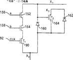
图7A显示了根据本发明的共振“与非”(NAND)门电路。更详细地,图5中的逻辑路径电路80被配置以通过将两个MOS(金属氧化物半导体)晶体管152、154串联来形成一个具有两输入端的“与非”(NAND)逻辑电路。第一MOS(金属氧化物半导体)晶体管152的门电路156与“与非”(NAND)门电路的输入端之一“a”相连,第二MOS(金属氧化物半导体)晶体管154的门电路158与另一个“与非”(NAND)门电路的输入端“b”相连。第一预充电路径160和第二预充电路径162均由半导体二极管(或与晶体管相连的二极管或其它等效件)来实现,两个路径二极管的阳极均与节点X2相连。第一预充电路径二极管160的阴极与节点X1相连,第二预充电路径二极管162的阴极与节点X3相连。Figure 7A shows a resonant NAND gate circuit in accordance with the present invention. In more detail, the logic path circuit 80 in FIG. 5 is configured to form a NAND logic circuit with two inputs by connecting two MOS (Metal Oxide Semiconductor)
图7B显示了说明“与非”(NAND)电路的工作状况的时序图。节点X2振荡时的共振频率与时钟信号92同步。当时钟信号92处于高电平170、172、174时,评估阶段被建立并且逻辑路径电路评估两个逻辑输入端“a”和“b”的状态。如果两个输入端都为高电平(在170期间),则用放电电流流入节点X2使节点X1放电。如果输入“a”或“b”中有一个为低电平(在172阶段),则节点X1保持预充电(并因此具有逻辑“1”)而反相晶体管164使节点X3放电给节点X2,致使节点X3变在逻辑“0”。在该周期的预充电阶段176、178、180期间,通过第一预充电路径160或第二预充电路径162将节点X1或X3中的一个预充电。FIG. 7B shows a timing diagram illustrating the operation of a NAND circuit. The resonant frequency when node X2 oscillates is synchronized with the
图7C显示了根据本发明的共振“或”(OR)门电路。在此电路中,逻辑路径电路具有两个部分。将第一部分配置成通过将两个MOS(金属氧化物半导体)晶体管190、192并联在节点X1与使逻辑路径工作的时钟晶体管90之间以形成一个具有两输入端的“或”(OR)电路。第二部分被配置成以在节点X4和时钟线92之间形成逻辑反相器194。Figure 7C shows a resonant OR gate circuit in accordance with the present invention. In this circuit, the logic path circuit has two parts. The first part is configured to form an OR circuit with two inputs by connecting two MOS (Metal Oxide Semiconductor) transistors 190, 192 in parallel between node X1 and the
第一预充电路径通过连接于节点X1和X2之间的二极管160来实现,第二预充电路径通过连接于节点X3和X2之间的二极管162来实现。节点X3和X2之间连接有反相晶体管164,其门电路与节点X1相连以使X1和X3在评估阶段期间具有互补逻辑电平。The first pre-charging path is realized by a
逻辑路径电路的第二部分,反相器194,及一个附加预充电路径196并联连接在节点X4与时钟线之间。反相器电路194包括串联连接的PMOS(P沟道金属氧化物半导体)晶体管200与NMOS(N沟道金属氧化物半导体)晶体管202,其中每一个晶体管的门电路相互连接并连接到节点X1,每一个晶体管的漏极相互连接以形成反相器194的输出节点X5。PMOS(P沟道金属氧化物半导体)晶体管200的源极与节点X4相连,NMOS(N沟道金属氧化物半导体)晶体管202的源极与预放电晶体管204的漏极相连,晶体管204的源极与时钟线92相连而其门电路与节点X2相连。反相器194的门电路与节点X1相连以接收“非或”(OR)电路的输出。预放电晶体管204的配置使其在时钟92为低电平而节点X2为高电平时(在图7D中的216或218期间)导通。预放电晶体管204的作用是在预充电阶段对节点X5放电。当时钟线92上的信号为高电平时,位于节点X4与时钟线之间的附加预充电路径196工作以使节点X4预充电。The second part of the logic path circuit, inverter 194, and an additional precharge path 196 are connected in parallel between node X4 and the clock line. The inverter circuit 194 includes a PMOS (P-channel Metal Oxide Semiconductor) transistor 200 and an NMOS (N-channel Metal Oxide Semiconductor) transistor 202 connected in series, wherein the gates of each transistor are connected to each other and to the node X1, The drains of each transistor are connected to each other to form the output node X5 of the inverter 194 . The source of the PMOS (P channel metal oxide semiconductor) transistor 200 is connected to the node X4, the source of the NMOS (N channel metal oxide semiconductor) transistor 202 is connected to the drain of the pre-discharge transistor 204, and the source of the transistor 204 It is connected to
图7D说明了图7C中电路的工作情况。在预充电阶段216、218,对节点X1、X3和X4预充电,并且因为节点X1被预充电以及用于反相器的预放电晶体管导通,使得预放电后的反相器的输出X5的电压接近于地电压。在下一个相位期间,即评估阶段210、212、214期间,时钟晶体管能使“或非”(NOR)电路根据输入端给“或非”(NOR)电路的156、158的逻辑状态来改变节点X1的状态。如果任何一个逻辑输入端为高电平,例如在210或214期间,则将节点X1放电到节点X2。如果没有一个输入端为高电平,例如在212期间,则将节点X3放电到节点X2(因为晶体管164导通),从而无论逻辑输入端为何状态,均向与节点X2相连的能量储存电路提供大致相同的能量。因此在评估阶段期间在节点X1上实现“或非”(NOR)功能。Figure 7D illustrates the operation of the circuit in Figure 7C. In the precharge phase 216, 218, the nodes X1, X3 and X4 are precharged, and because the node X1 is precharged and the predischarge transistor for the inverter is turned on, so that the predischarged inverter output X5 voltage close to ground. During the next phase, the evaluation phase 210, 212, 214, the clock transistor enables the NOR circuit to change node X1 according to the logic state of the input to the NOR
此外,在评估阶段期间,如果“或非”(NOR)电路的输出为高电平,由于节点X1保持预充电,则反相器194的输出X5保持低电平。但是,如果“或非”(NOR)电路的输出为低电平,由于节点X1被预放电,则反相器194的输出X5被充电至高电平,这是因为反相器194的PMOS(P沟道金属氧化物半导体)晶体管200将节点X5与在预充电阶段被充电至高电平的节点X4相连。通过与时钟线连接的时钟驱动电路(未显示出)恢复反相器电路的工作能量。Also, during the evaluation phase, if the output of the NOR circuit is high, the output X5 of the inverter 194 remains low since node X1 remains precharged. However, if the output of the NOR circuit is low, the output X5 of the inverter 194 is charged high because the node X1 is pre-discharged because the PMOS of the inverter 194 (P Trench MOS) transistor 200 connects node X5 to node X4 charged to a high level during the precharge phase. The operating energy of the inverter circuit is recovered by a clock driving circuit (not shown) connected to the clock line.
图8表示了根据本发明结合有初始化电路42,能量储存电路40以及自适应电路44的共振逻辑电路46的实施例。在该图中,逻辑路径80和预充电路径86、88被显示为方框以简化图示。可将逻辑电路,例如图7A和图7C中所示的“与非”(NAND)或“或”(OR)电路,代入所示的逻辑路径80中,可将图7A和7C中所示的预充电电路代入所示的预充电路径86、88中。FIG. 8 shows an embodiment of a
如图2A所示的初始化电路42,包括与复位线48相连的反相器230;一对预充电晶体管232、234,该预充电晶体管232、234的门电路与反相器230的输出相连;以及放电晶体管236,该放电晶体管236的门电路与复位线48相连。预充电晶体管232连接于主电源的供给节点VDD与节点X1之间,以对节点X1预充电,放电晶体管236连接于节点X2与地线之间,以对节点X2进行接地放电。The
当复位线48为高电平时,放电晶体管236导通以对节点X2进行放电。与此同时,反相器电路230将复位信号48反相并将预充电晶体管232、234的门电路驱动至低电平,以使它们导通。这使得节点X1与节点X3被预充电至一接近于供给节点(Vdd-Vt)的电压。当复位线48返回低电平时,节点X2以由负载电容C0 96、C1100和C2 98以及逻辑路径电路和电感器L 40中的损失所确定的共振频率开始振荡。因为节点X1的负载电容与节点X3的负载电容大致相等,所以无论逻辑电路46的逻辑输入端82为何状态,振荡频率都几乎恒定。When the
自适应电路44用于检测何时预充电节点未被充电至足够接近于主电源电压。这表示需要向逻辑电路供应更多的能量,因为一些能量以热的形式损耗掉了。一旦确定预充电电压已经降至低于预定阈值,自适应电路44就在工作周期的预充电阶段通过给节点X1和节点X3增加能量来作出响应。通过此方式,电源补偿电路中的耗散损失。
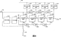
图9显示了根据本发明的一种管线式逻辑电路的方框图。管线式逻辑电路通常被被多次需要,因为没有足够的时间在逻辑电路的单个状态中评估复杂的逻辑功能。举例来说,如果图9所示的共振电路和时钟以300MHz的频率工作,那么逻辑路径仅有约1.6ns的时间来确定其输出。对于一个象“与非”(NAND)或“或非”(NOR)功能这样的单一功能来说,这么长的时间可能是足够的,但对于象具有许多输入的二进制加法器电路的复杂功能来说,并没有足够的时间来评估所涉及的逻辑功能。因此,必须将用于此功能的电路分成多个管线级。尽管增加了用于计算逻辑功能结果的时间,但管线可以一次拥有许多不同的逻辑功能,每个功能处于不同的管线级。此技术不仅给予足够的时间来计算复杂的逻辑功能,而且提高了逻辑电路的处理量。FIG. 9 shows a block diagram of a pipelined logic circuit according to the present invention. Pipelined logic circuits are often required multiple times because there is not enough time to evaluate complex logic functions in a single state of the logic circuit. For example, if the resonant circuit and clock shown in Figure 9 are operated at 300MHz, then the logic path has only about 1.6ns to determine its output. This long time may be sufficient for a single function like a NAND or NOR function, but is not sufficient for a complex function like a binary adder circuit with many inputs. That said, there wasn't enough time to evaluate the logic functions involved. Therefore, the circuitry used for this function must be divided into multiple pipeline stages. Despite the increased time used to compute the results of logic functions, a pipeline can have many different logic functions at once, each at a different pipeline stage. This technology not only gives enough time to calculate complex logic functions, but also improves the processing capacity of logic circuits.
图9显示了此管线式逻辑电路的一个实施例。在该图中,共振逻辑电路级A 46a、B 46b、C 46c、D 46d连接在一起,前一级的输出即为下一邻接级的输入。每一个共振级均与一个初始化和自适应电路块252、254、256连接,并且每一级,A、B、C或D,分别接收时钟信号CLK、CLK1、CLK2、CLK3以及振荡功率信号X2A、X2B、X2C、X2D。但是,除第一级外的其它共振级的时钟信号和振荡功率信号都相对于前一级具有一个延迟。在时钟路径中的每个延迟258、260、262必须与振荡功率信号路径中的每个延迟264、266、268分别精确匹配,使得二者都处于每一级中的锁相和锁频。同时,管线式电路中还包括一个鉴相器270以确定时钟信号92与节点X2A上的共振信号之间的相位差。鉴相器的输出将提供给调谐电路272,此调谐电路272调整节点X2上共振信号的相位以保持在时钟和共振功率信号之间的相位同步。Figure 9 shows an embodiment of this pipelined logic circuit. In this figure, resonant logic circuit stages A 46a,
插入共振级间的延迟258、260、262的大小稍微大于共振级在其功率周期(power cycle)的评估阶段期间计算其逻辑输出所用的时间。按此方式,当后继共振级开始其评估阶段时,稳定的输出α1、α2、α3可提供给该后继共振级。经过n个延迟后,其中n表示共振级的数量,可获得从管线的输出274。在一个实施例中,一旦从管线的最后共振级D获得输出274,第一共振级A便可开始其预充电阶段。在另一实施例中,在第一共振级A开始预充电阶段的同时,管线的最后共振级开始计算其结果。这使得共振级的预充电阶段与评估阶段重叠,从而每n个延迟产生一个新的计算结果,其中n表示共振级的数量。The magnitude of the
虽然参照某些最佳实施例相当详细地描述了本发明,但其它实施方式也是可能的。因此,所附权利要求的本质和范围不应局限于这里所包含的最佳实施方式的描述。While the invention has been described in considerable detail with reference to certain preferred embodiments, other embodiments are possible. Therefore, the spirit and scope of the appended claims should not be limited to the description of the best mode contained herein.
Claims (15)
Applications Claiming Priority (2)
| Application Number | Priority Date | Filing Date | Title |
|---|---|---|---|
| US09/614,494 US6448816B1 (en) | 2000-07-11 | 2000-07-11 | Resonant logic and the implementation of low power digital integrated circuits |
| US09/614,494 | 2000-07-11 |
Publications (1)
| Publication Number | Publication Date |
|---|---|
| CN1663125A true CN1663125A (en) | 2005-08-31 |
Family
ID=24461477
Family Applications (1)
| Application Number | Title | Priority Date | Filing Date |
|---|---|---|---|
| CN018154573A Pending CN1663125A (en) | 2000-07-11 | 2001-07-11 | Resonant logic and the implementation of low power digital integrated circuits |
Country Status (8)
| Country | Link |
|---|---|
| US (2) | US6448816B1 (en) |
| EP (1) | EP1319271A4 (en) |
| JP (1) | JP2004503165A (en) |
| KR (1) | KR20030029105A (en) |
| CN (1) | CN1663125A (en) |
| AU (1) | AU2001273398A1 (en) |
| TW (1) | TW531961B (en) |
| WO (1) | WO2002005426A1 (en) |
Cited By (3)
| Publication number | Priority date | Publication date | Assignee | Title |
|---|---|---|---|---|
| CN101997539A (en) * | 2010-11-22 | 2011-03-30 | 北京时代民芯科技有限公司 | Programmable logic circuit |
| CN106571804A (en) * | 2015-10-09 | 2017-04-19 | 张伟林 | Standard interface circuit of high-impedance digital phase detector output stage |
| CN109831199A (en) * | 2019-03-11 | 2019-05-31 | 福州大学 | A kind of IG reversible logic gate circuit applied to reversible logic circuits |
Families Citing this family (12)
| Publication number | Priority date | Publication date | Assignee | Title |
|---|---|---|---|---|
| US6552574B1 (en) * | 2002-03-01 | 2003-04-22 | Piconetics, Inc. | Low power dynamic logic gate with full voltage swing operation |
| US6742132B2 (en) | 2002-04-04 | 2004-05-25 | The Regents Of The University Of Michigan | Method and apparatus for generating a clock signal having a driven oscillator circuit formed with energy storage characteristics of a memory storage device |
| GB0210625D0 (en) * | 2002-05-09 | 2002-06-19 | Paradigm Design Systems | Control of guard flops |
| US8277373B2 (en) * | 2004-04-14 | 2012-10-02 | Usgi Medical, Inc. | Methods and apparaus for off-axis visualization |
| US20070202912A1 (en) * | 2006-02-28 | 2007-08-30 | Helix Micro, Inc. | Transmission Line Power Supply for Energy Efficient Circuits |
| US20080061836A1 (en) * | 2006-08-22 | 2008-03-13 | International Business Machines Corporation | Current Mirror and Parallel Logic Evaluation |
| US7973565B2 (en) * | 2007-05-23 | 2011-07-05 | Cyclos Semiconductor, Inc. | Resonant clock and interconnect architecture for digital devices with multiple clock networks |
| US8502569B2 (en) * | 2009-10-12 | 2013-08-06 | Cyclos Semiconductor, Inc. | Architecture for operating resonant clock network in conventional mode |
| EP2779457B1 (en) | 2013-03-15 | 2018-08-29 | Dialog Semiconductor B.V. | Method for charge sharing/reuse of electronic circuits |
| US10340895B2 (en) | 2017-09-25 | 2019-07-02 | Rezonent Corporation | Reduced-power electronic circuits with wide-band energy recovery using non-interfering topologies |
| US11023631B2 (en) | 2017-09-25 | 2021-06-01 | Rezonent Corporation | Reduced-power dynamic data circuits with wide-band energy recovery |
| CN110880932B (en) * | 2019-11-12 | 2023-05-12 | 宁波大学 | Logic circuit approximation implementation method |
Family Cites Families (11)
| Publication number | Priority date | Publication date | Assignee | Title |
|---|---|---|---|---|
| US5559463A (en) * | 1994-04-18 | 1996-09-24 | Lucent Technologies Inc. | Low power clock circuit |
| US5506519A (en) * | 1994-06-03 | 1996-04-09 | At&T Corp. | Low energy differential logic gate circuitry having substantially invariant clock signal loading |
| JP3313276B2 (en) * | 1995-03-15 | 2002-08-12 | 株式会社東芝 | MOS gate circuit and power supply method thereof |
| US5559478A (en) | 1995-07-17 | 1996-09-24 | University Of Southern California | Highly efficient, complementary, resonant pulse generation |
| GB9707349D0 (en) * | 1997-04-11 | 1997-05-28 | Univ Waterloo | A dynamic current mode logic family |
| JP3460956B2 (en) * | 1997-09-05 | 2003-10-27 | 日本電信電話株式会社 | Adiabatic charging logic |
| US6255853B1 (en) * | 1997-09-29 | 2001-07-03 | Texas Instruments Incorporated | Integrated circuit having dynamic logic with reduced standby leakage current |
| JP3080062B2 (en) * | 1998-04-06 | 2000-08-21 | 日本電気株式会社 | Semiconductor integrated circuit |
| JPH11340812A (en) * | 1998-05-22 | 1999-12-10 | Mitsubishi Electric Corp | Semiconductor device |
| JP3123516B2 (en) * | 1998-08-14 | 2001-01-15 | 日本電気株式会社 | Semiconductor device and method of driving semiconductor device |
| US6246266B1 (en) * | 1999-09-24 | 2001-06-12 | Texas Instruments Incorporated | Dynamic logic circuits using selected transistors connected to absolute voltages and additional selected transistors connected to selectively disabled voltages |
-
2000
- 2000-07-11 US US09/614,494 patent/US6448816B1/en not_active Expired - Fee Related
-
2001
- 2001-07-11 TW TW090116982A patent/TW531961B/en not_active IP Right Cessation
- 2001-07-11 WO PCT/US2001/021966 patent/WO2002005426A1/en not_active Ceased
- 2001-07-11 CN CN018154573A patent/CN1663125A/en active Pending
- 2001-07-11 KR KR10-2003-7000442A patent/KR20030029105A/en not_active Withdrawn
- 2001-07-11 EP EP01952669A patent/EP1319271A4/en not_active Withdrawn
- 2001-07-11 JP JP2002509172A patent/JP2004503165A/en active Pending
- 2001-07-11 AU AU2001273398A patent/AU2001273398A1/en not_active Abandoned
- 2001-09-27 US US09/967,189 patent/US6559681B1/en not_active Expired - Fee Related
Cited By (5)
| Publication number | Priority date | Publication date | Assignee | Title |
|---|---|---|---|---|
| CN101997539A (en) * | 2010-11-22 | 2011-03-30 | 北京时代民芯科技有限公司 | Programmable logic circuit |
| CN101997539B (en) * | 2010-11-22 | 2012-08-22 | 北京时代民芯科技有限公司 | Programmable logic circuit |
| CN106571804A (en) * | 2015-10-09 | 2017-04-19 | 张伟林 | Standard interface circuit of high-impedance digital phase detector output stage |
| CN106571804B (en) * | 2015-10-09 | 2023-08-11 | 张伟林 | Standard interface circuit of high-resistance digital phase discriminator output stage |
| CN109831199A (en) * | 2019-03-11 | 2019-05-31 | 福州大学 | A kind of IG reversible logic gate circuit applied to reversible logic circuits |
Also Published As
| Publication number | Publication date |
|---|---|
| KR20030029105A (en) | 2003-04-11 |
| EP1319271A1 (en) | 2003-06-18 |
| EP1319271A4 (en) | 2005-04-20 |
| WO2002005426A1 (en) | 2002-01-17 |
| US6559681B1 (en) | 2003-05-06 |
| AU2001273398A1 (en) | 2002-01-21 |
| JP2004503165A (en) | 2004-01-29 |
| US6448816B1 (en) | 2002-09-10 |
| TW531961B (en) | 2003-05-11 |
Similar Documents
| Publication | Publication Date | Title |
|---|---|---|
| CN1663125A (en) | Resonant logic and the implementation of low power digital integrated circuits | |
| US6028453A (en) | Charge recycling differential logic (CRDL) circuit having true single-phase clocking scheme | |
| US6307425B1 (en) | Clocking scheme and charge transfer switch for increasing the efficiency of a charge pump or other circuit | |
| US5701093A (en) | Adiabatic MOS logic and power supplying method and apparatus | |
| US6016065A (en) | Charges recycling differential logic(CRDL) circuit and storage elements and devices using the same | |
| US20080204124A1 (en) | Fine-Grained Power Management of Synchronous and Asynchronous Datapath Circuits | |
| US6864732B2 (en) | Flip-flop circuit with reduced power consumption | |
| JP4034781B2 (en) | Clock generator for integrated circuits | |
| US6211701B1 (en) | Low power line switching circuit, device and method | |
| US7116137B2 (en) | Method and system for reducing power consumption in digital circuitry using charge redistribution circuits | |
| US20130141073A1 (en) | Charge recycling a 1 of n ndl gate with a time varying power supply | |
| CN1650522A (en) | Low Power Dynamic Logic Gates with Full Voltage Swing Operation | |
| US6812745B1 (en) | Resonant logic and the implementation of low power digital integrated circuits | |
| Watkins | A low-power multiphase circuit technique | |
| Parthasarathy et al. | Double pass-transistor logic for high performance wave pipeline circuits | |
| US20030005017A1 (en) | Simultaneous dual rail static carry-save-adder circuit | |
| CN1808448A (en) | Rotary clock logic | |
| KR20000067503A (en) | reversible adiabatic logic circuit and pipeline reversible adiabatic logic apparatus employing the same | |
| WO2025076502A1 (en) | Quasi-adiabatic logic | |
| JP2003264453A (en) | Clock abnormality detection circuit | |
| Akers et al. | Adiabatic circuits for low power logic | |
| Kim et al. | An 8-b nRERL microprocessor for ultra-low-energy applications | |
| Voss et al. | Adiabatic charging of long interconnects | |
| JPS607860B2 (en) | integrated frequency divider | |
| Priya et al. | Asynchronous Domino Logic Pipeline Based ECRL |
Legal Events
| Date | Code | Title | Description |
|---|---|---|---|
| C06 | Publication | ||
| PB01 | Publication | ||
| C10 | Entry into substantive examination | ||
| SE01 | Entry into force of request for substantive examination | ||
| C02 | Deemed withdrawal of patent application after publication (patent law 2001) | ||
| WD01 | Invention patent application deemed withdrawn after publication |