CN1607994A - Method and apparatus for applying downward force on wafer during cmp - Google Patents
Method and apparatus for applying downward force on wafer during cmp Download PDFInfo
- Publication number
- CN1607994A CN1607994A CNA028262301A CN02826230A CN1607994A CN 1607994 A CN1607994 A CN 1607994A CN A028262301 A CNA028262301 A CN A028262301A CN 02826230 A CN02826230 A CN 02826230A CN 1607994 A CN1607994 A CN 1607994A
- Authority
- CN
- China
- Prior art keywords
- load cell
- wafer
- air bag
- power
- axle
- Prior art date
- Legal status (The legal status is an assumption and is not a legal conclusion. Google has not performed a legal analysis and makes no representation as to the accuracy of the status listed.)
- Pending
Links
Images

Classifications
-
- B—PERFORMING OPERATIONS; TRANSPORTING
- B24—GRINDING; POLISHING
- B24B—MACHINES, DEVICES, OR PROCESSES FOR GRINDING OR POLISHING; DRESSING OR CONDITIONING OF ABRADING SURFACES; FEEDING OF GRINDING, POLISHING, OR LAPPING AGENTS
- B24B37/00—Lapping machines or devices; Accessories
- B24B37/27—Work carriers
- B24B37/30—Work carriers for single side lapping of plane surfaces
-
- H—ELECTRICITY
- H01—ELECTRIC ELEMENTS
- H01L—SEMICONDUCTOR DEVICES NOT COVERED BY CLASS H10
- H01L21/00—Processes or apparatus adapted for the manufacture or treatment of semiconductor or solid state devices or of parts thereof
- H01L21/02—Manufacture or treatment of semiconductor devices or of parts thereof
- H01L21/04—Manufacture or treatment of semiconductor devices or of parts thereof the devices having at least one potential-jump barrier or surface barrier, e.g. PN junction, depletion layer or carrier concentration layer
- H01L21/18—Manufacture or treatment of semiconductor devices or of parts thereof the devices having at least one potential-jump barrier or surface barrier, e.g. PN junction, depletion layer or carrier concentration layer the devices having semiconductor bodies comprising elements of Group IV of the Periodic System or AIIIBV compounds with or without impurities, e.g. doping materials
- H01L21/30—Treatment of semiconductor bodies using processes or apparatus not provided for in groups H01L21/20 - H01L21/26
- H01L21/302—Treatment of semiconductor bodies using processes or apparatus not provided for in groups H01L21/20 - H01L21/26 to change their surface-physical characteristics or shape, e.g. etching, polishing, cutting
- H01L21/304—Mechanical treatment, e.g. grinding, polishing, cutting
-
- B—PERFORMING OPERATIONS; TRANSPORTING
- B24—GRINDING; POLISHING
- B24B—MACHINES, DEVICES, OR PROCESSES FOR GRINDING OR POLISHING; DRESSING OR CONDITIONING OF ABRADING SURFACES; FEEDING OF GRINDING, POLISHING, OR LAPPING AGENTS
- B24B49/00—Measuring or gauging equipment for controlling the feed movement of the grinding tool or work; Arrangements of indicating or measuring equipment, e.g. for indicating the start of the grinding operation
- B24B49/16—Measuring or gauging equipment for controlling the feed movement of the grinding tool or work; Arrangements of indicating or measuring equipment, e.g. for indicating the start of the grinding operation taking regard of the load
Abstract
An apparatus for applying a wafer to a polishing belt during a CMP operation includes a spindle having an upper end and a lower end. A wafer carrier is coupled to the lower end of the spindle. A linear force generator is disposed at the upper end of the spindle. A load cell is positioned between the linear force generator and the upper end of the spindle. A controller is coupled to the load cell for controlling the force applied by the linear force generator. A method for applying downward force on a wafer during CMP also is described.
Description
Technical field
The present invention relates to chemical-mechanical planarization (CMP) technology and, more specifically, relate to a kind of method and a kind of equipment that is used for wafer being applied to polished surface that is used on wafer, applying downward power in CMP operation in the CMP process.
Background technology
In making semiconductor device, need to carry out chemical-mechanical planarization (CMP) operation.Usually, IC apparatus is multi-ply construction.In substrate layer, form transistor unit with diffusion zone.In layer subsequently, interconnected metallized thread is patterned and be electrically connected to this transistor unit to produce the device with expectation function.As everyone knows, patterned conductive layer is by dielectric material, and for example silica and other conductive layer insulate.Formation along with increasing metal layer and relevant dielectric layer just more and more needs the planarization dielectric material.If there is not planarization, so further the manufacturing meeting of metal layer becomes difficult more because of the variation of surface topography.In other were used, metallization line patterns was formed in the dielectric material, then, carried out the metal CMP operation to remove unnecessary metal.
Chemical-mechanical planarization (CMP) system is generally used for polished wafer as stated above.The CMP system generally includes and is used to transport and the component of a system on polished wafer surface.This member can be, for example, and track polishing pad or linear strip polishing pad.This polishing pad normally cooperates other materials (for example stainless steel band) to make by polyurethane material or polyurethane.In operation, move this band shape polishing pad and also then the liquid pulp material is applied and is dispersed on the surface of this band shape polishing pad.After being coated in the liquid slurry on the banded polishing pad, this band shape polishing pad moves with a speed of setting, and wafer is moved down to the surface of this band shape polishing pad.With the method, the wafer surface of desire planarization is smoothedization substantially, is used to polish timber as sand paper.Then this wafer is cleaned in chip cleaning system.
Figure 1A shows the linear planarization device 10 that is generally used in the CMP system.This linear planarization device 10 removes semiconductor wafer 16 lip-deep material polishings.The one or more layer that the material that is removed can be the substrate material of wafer 16 or forms on wafer 16.This layer is usually included in the CMP operating process one or more the material of arbitrary type that forms or exist, for example, and dielectric material, silicon nitride, metal (for example, aluminium and copper), metal alloy, semi-conducting material etc.Usually, CMP can be used for the one or more layer superficial layers with planarization wafer 16 on the polished wafer 16.
The surperficial linear mobile sand belt 12 that this linear planarization device 10 uses with respect to wafer 16.Sand belt 12 is the continuous bands around roller 20 rotations.Thereby this roller drives rotatablely moving of roller 20 by motor usually makes sand belt 12 move linearly 22 with respect to wafer 16.
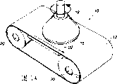
Figure 1B shows the axle driven unit 30 that in the CMP system 10 that is used in (as above shown in Figure 1A) wafer 16 is applied to the routine on the sand belt.Axle driven unit 30 comprises the rubbing head 18 that is connected on the axle 42.Axle 42 is connected on the power amplifier 34, and an end of power amplifier 34 is connected on the hinge 40 and the other end is connected on the air cylinder 32.Power amplifier 34 is generally the aluminium arm of machining, and this aluminium arm moves in the mode similar to lever, thereby is amplified on the axle 42 by the power that air cylinder 32 applies.Axle 42 promotes rubbing head 18 downwards then, and rubbing head 18 then is applied on the wafer 16 pressure to polish action (shown in Figure 1A).
Usually, can apply the pressure of 3psi (pound/square inch) to wafer 16 by axle driven unit 30 to the 10psi scope.Unfortunately, when pressure was lower than 3psi, axle driven unit 30 can not apply consistent, controlled pressure.Usually by the control of pneumatic servo valve, this pneumatic servo valve uses the feedback from the load cell 36 that is positioned at rubbing head 18 to air cylinder 32.Problem be the weight of axle, rubbing head and other member except axle not by any other member supports.This make apply very more unstable than being connected to the little downward power of weight on the cylinder 32.Simultaneously, owing to power amplifier 34, a small amount of pressure of doing in cylinder 32 places is regulated and can be made rubbing head 18 applied pressures that big variation takes place, and therefore the control to pressure is very difficult.Under specific circumstances, can not control applying of little power and hinder the slight contact polishing pad of wafer downwards.Because axle driven unit 30 makes this situation often take place for intrinsic the overregulating that specified pressure is set.For example, if desire is applied to the pressure of 4psi on the wafer, the pressure that applies 5psi so usually is to offset the frictional force in each parts of axle driven unit 30 and to move described axle.Therefore, it is problematic using conventional pressure application system that low polish pressure is applied on the wafer.
In addition, because air cylinder 32 is connected indirectly with the remainder of axle driven unit 30, the stability that therefore rubbing head 18 often takes place reduces.Therefore, often the inaccessible pressure that the polish pressure of unanimity is especially low is applied on the wafer.
Therefore, need a kind of equipment that can overcome the problems of the prior art, it optimizes the control that is applied to the polish pressure on the wafer in the CMP system by rubbing head by the application devices with downward force.
Summary of the invention
In general, the present invention satisfies these demand by the power that optimal control in chemical-mechanical planarization (CMP) polishing operation process applies downwards.Should be understood that the present invention can be used in various manners, comprises operation, equipment, system, device or method.Several innovative embodiment of the present invention will be described below.
According to an aspect of the present invention, provide a kind of being used for wafer to be applied to equipment on the polished surface in CMP operation.This equipment comprises the axle with top and bottom.Chip carrier is connected on the lower end of this axle.Linear force generator is arranged on the upper end of described axle.Load cell is arranged between the upper end of linear force generator and this axle.Controller is connected to the power that is applied by linear force generator with control on the load cell.
In one embodiment, described linear force generator comprises the lower shoe (lower plate) that is arranged on the load cell and is supported on the upper plate (upper plate) of lower shoe top.Linear force generator also comprises the air bag that is arranged between lower shoe and the upper plate.In another embodiment, load cell plate is connected on the upper end of axle, and load cell is arranged on the load cell plate.
According to a further aspect in the invention, a kind of method that is used for applying to wafer in chemical-mechanical planarization (CMP) process downward power is disclosed.In the method, linear downward power is applied to the upper end of axle.This axle has the chip carrier that is connected to its lower end.This method is also monitored the linear downward power that is applied to the axle upper end.
The present invention has lot of advantages.Be the most significantly, be suitable for optimal control and be applied to the equipment of the linear downward power on the wafer, can improve control widely the polish pressure that is used for CMP by generation.Especially, the power generating assembly can be connected to the upper end of axle, and the lower end of axle can be connected on the chip carrier.This structure enables direct linear application of force on the wafer.By this way, can enlarge the scope and low the apply power of enhancing on wafer of the power of the unanimity that is applied.In addition, power application devices described herein has increased the stability of chip carrier, and it further optimizes processing of wafers.Therefore, the power application devices can be controlled wafer polishing pressure highly beneficially and improve the treatment effeciency of wafer.
Should be understood that above describe, in general terms and following detailed only for exemplary and indicative, rather than to the desired restriction of the present invention of claim.
Description of drawings
Be incorporated into this accompanying drawing that also constitutes the part of this explanation and show exemplary embodiment of the present invention, and be used from explanation principle of the present invention with description one.
Figure 1A shows the linear planarization equipment that is generally used in the CMP system.
Figure 1B shows conventional axle driven unit, and it is used in the CMP system (as above shown in Figure 1A) wafer is applied on the sand belt.
Fig. 2 A shows the CMP system according to one embodiment of the invention.
Fig. 2 B shows the force applying assembly according to one embodiment of the invention.
Fig. 2 C shows the power generating assembly of improvement that has the backspring structure of replacement according to one embodiment of the invention.
Fig. 2 D comprises the power generating assembly according to the improvement of one embodiment of the invention.
Fig. 3 shows the operational block diagram according to the force applying assembly of one embodiment of the invention.
The specific embodiment
Describe several exemplary embodiments of the present invention in detail referring now to accompanying drawing.In superincumbent " background technology " part Figure 1A and 1B have been described.Described the equipment that applies downward power although should be understood that following examples, can be inverted following examples to apply power upwards.In being described below, a plurality of details have been set forth so that understand the present invention fully.Yet those skilled in the art should be appreciated that lacking under the situation of some or all these details still can implement the present invention.In other embodiments, known process operation is not described in detail to avoid unnecessarily obscuring the present invention.
Fig. 2 A shows chemical-mechanical planarization (CMP) system 100 according to one embodiment of the invention.Carrier head 106 is parts of force applying assembly 118 (shown in Fig. 2 B), and it is used in the wafer polishing operation wafer 104 is fixed and is held in place.Sand belt 102 walks around rotating drum 112a and 112b forms continuous ring.Should be understood that sand belt 102 can be the structure of any suitable type, for example the polishing pad of individual layer, the polishing pad that supports by stainless steel layer, multilayer polishing structure (for example, at the polishing pad on the cushion and this cushion attached to stainless steel layer on).Be also to be understood that principle described here also is applicable to the CMP system of non-banding pattern, for example whirligig.In one embodiment, sand belt 102 is the individual layer polyurethane polishing pads that are used for linear CMP system.Sand belt 102 is rotated by 108 indicated directions with the about 400 feet speed edge of per minute usually.Yet this speed changes according to concrete CMP operation.
When sand belt 102 rotations, the polishing fluid slurry can apply and be dispersed on the surface of this sand belt 102.Then carrier head 106 can be used for wafer 104 is reduced on the surface of sand belt 102 of rotation.Below with reference to Fig. 2 B force applying assembly 118 is described in further detail.Platen 110 can support sand belt 102 in polishing process.Platen 110 can use the support of any suitable type, and for example air supports.By this way, the predetermined surface of planarization of wanting of wafer 104 can be in uniform mode by smoothing substantially.
In some cases, the CMP operation is used for for example material of copper (or other metal) of planarization, and in other cases, it can be used for removing the combination layer of dielectric layer or dielectric material and copper.Can change the speed of planarization by the adjusting polish pressure.Polishing speed is proportional with the amount that is applied to the polish pressure of antagonism platen 110 on the polishing pad by carrier head 106 and wafer 104 usually.By handling polishing speed effectively, remove the material of scheduled volume from the surface of wafer 104.After having finished polishing operation, carrier head 106 can be used for wafer 104 is removed from sand belt 102 rises.Wafer 104 can be sent in the wafer purging system then.Therefore stable and to apply downward power neatly be extremely important for wafer manufacture efficiently by carrier head 106.
Fig. 2 B shows the force applying assembly 118 according to one embodiment of the invention.In this embodiment, force applying assembly 118 comprises chip carrier 106 that is connected to axle 126 lower ends and the power generating assembly 120 that is connected to axle 126 upper ends.In one embodiment, chip carrier 106 along substantially direct vertical line be positioned at power generating assembly 120 and axle 126 below.It should be understood that axle can be any suitable shape, as long as can be connected to power generating assembly 120 on the chip carrier 106.In one embodiment, axle 126 has the shape of substantially cylindrical.The lower end of axle 126 is connected on the chip carrier 106 and its upper end is connected on the power generating assembly 120.Should be understood that axle 126 can be any suitable dimensions, this depends on the structure of desire use in CMP system 100.
Should be understood that air bag 122 can use any suitable gas or liquid to exert pressure to chip carrier 106.In one embodiment, with the clean air of cleaning air bag 122 is expanded.Used hereinly can be replaced by any suitable gas or liquid, for example nitrogen etc. for quoting of " air ".Air duct 138 is connected on the air bag 122 by the hole in the upper plate 136.Air duct 138 is connected on the servo valve 140, and servo valve 140 controls are to the air of air bag 122 inputs and the air of exporting from air bag 122.Air duct 138 is also connected on the rapid exhaust 143 that can discharge air fast.Should be understood that rapid exhaust 143 can be any suitable air releasing device, for example solenoid, rapid escape valve etc.Servo valve 140 is connected on input 144 (entering servo valve) and the output 142 (going out white servo valve).Servo valve 140 can be used for controlling the air input and output from air bag 122.Perhaps, servo amplifier comparator 145 can be monitored the amount by the detected downward power of load cell 124, and this load cell 124 is used to control servo valve 140 to be provided with and/or to keep by air bag and be applied to quantitative downward power on the axle 126.Here servo amplifier comparator 145 and servo valve 140 are also referred to as controller.Therefore, controller can be connected to the power that is applied by linear force generator 121 with control on the load cell.Further describe the operation of monitoring and applying downward power below with reference to Fig. 3.
When air was from servo valve 140 input air bags 122, the volume of air bag 122 increased and expands.When air bag 122 expanded, it pressed upper plate 136 and lower shoe 132.In one embodiment, upper plate 136 can be stabilized, and therefore upper plate 136 can not move when air bag 122 expands.Lower shoe is shifted onto for 132 times on the load cell 124, and load cell 124 passes to load cell plate 130 with downward power.Load cell plate 130 directly passes to axle 126 with downward power.By using downward power, the chip carrier 106 that axle 126 moves down and promote to have wafer leans against on the polishing pad to carry out the wafer polishing operation.Therefore, in one embodiment, the downward power of direct linearity that is applied by air bag 122 passes to chip carrier to carry out wafer polishing.
Air pressure in the adjustable solar term capsule 122 is so that air bag applies the power of scheduled volume on axle.When the air pressure in the air bag 122 reduces, spring 134 (when in the air input air bag 122, it expands) thus shrink and reduce the power that is applied on the lower shoe 132.When this happens, the downward power that is applied on the chip carrier 106 reduces, thereby the polish pressure that is applied in the CMP process on the wafer reduces.Because apply, so the minor adjustment that is applied on the air bag 122 passes to chip carrier 106 in the mode of direct linearity in the mode that does not make power downward under the situation of amplifier firmly with direct linearity.Force applying assembly 118 and conventional power bringing device specific energy are mutually stably exerted pressure to wafer in the larger context.
Fig. 2 C shows the power generating assembly 120 ' of improvement according to having of one embodiment of the invention of interchangeable backspring structure.In this embodiment, power generating assembly 120 ' has the load cell plate 130 of the upper end of axle of being connected to 126.Load cell springs 148 is the compression springs that are positioned at load cell plate 130 belows.Load cell springs 148 is connected with reverse arm, and this reverse arm passes load cell plate 130 and is connected on the lower shoe 132.By using compression spring 148, reverse arm is moved lower shoe 132 on the load cell 124 to, and load cell 124 is between lower shoe 132 and load cell plate 130.Backspring 146 is positioned at the below of lower shoe 132 and is connected on the reverse arm, and this reverse arm passes lower shoe 132 and is connected on the upper plate 136.By using compression spring 146, reverse arm is moved upper plate 136 on the air bag 122 to, and air bag 122 is between lower shoe 132 and upper plate 136.Bladder spacer 144 limits the compression ratio of air bag 122 by the contraction in space between restriction upper plate 136 and the lower shoe 132.
When air bag 122 expanded, it pressed upper plate 136 and lower shoe 132.Lower shoe is shifted onto for 132 times on the load cell 124, and load cell 124 is exerted pressure to load cell plate 130.Moving downward of lower shoe 132 expanded support spring 146.Load cell plate 130 will be directly passed to axle 126 by the pressure that air bag 122 produces.The chip carrier 106 that axle 126 promotions have wafer leans against on the polishing pad to carry out the wafer polishing operation.
When air bag 122 shrank, the power that is applied on upper plate 136 and the lower shoe 136 (2) reduced, so spring 146 shrinks.When this happens, the downward pressure that is applied by air bag 122 reduces, and the downward power that axle 126 is applied on the chip carrier 106 reduces thereupon.Therefore the minimizing at the pressure on the chip carrier 106 makes the polish pressure that is applied in the CMP process on the wafer reduce.Because apply in the mode that does not make power downward under the situation of amplifier firmly with direct linearity, so the minor adjustment that is applied on the air bag 122 is directly passed to chip carrier 106.This force applying assembly and conventional power bringing device specific energy are mutually stably exerted pressure to wafer in the larger context.
Fig. 2 D comprises the power generating assembly 120 according to the improvement of one embodiment of the invention ".In this embodiment, power generating assembly 120 " 26S Proteasome Structure and Function with power generating assembly 120 ', but it has reverse indicator 162, and it passes upper plate 136 and is connected with lower shoe 132.This reverse indicator 162 can be notified to control pressurer system with reversing of mechanism.The sensor that is positioned at the reverse indicator top detects the position of reverse indicator 162, and moves to show that lower shoe 132 reverses fully.In addition, " comprise load cell amplifier out 164, it makes the servo amplifier comparator receive the load cell signal of amplifying to power generating assembly 120.Rotation pipe box 126a can randomly be installed on the axle 126.Rotation pipe box 126a makes axle 126 rotations and allow air in one embodiment and/or be vacuum transferred on the carrier head.Should be understood that the axle of describing in this embodiment 126 (as with reference to described in the figure 2B to 3) selectively comprises rotation pipe box 126a.
Fig. 3 shows the operation box Figure 200 according to the force applying assembly 118 of one embodiment of the invention.In block diagram 200, when air is input to air bag 122, air bag 122 expand and under shift onto on the load cell 124.Load cell 124 detects the power that is applied by air bag 122 and passes through load cell amplifier 164 and sends the power measuring-signals to servo amplifier comparator 145, and servo amplifier comparator 145 is presented at the amount of the detected linear downward force in load cell 124 places.Signal from load cell 124 is a low pressure, so load cell amplifier 164 is put this measuring-signal energetically.Servo amplifier comparator 145 receives from the signal (this signal is aanalogvoltage in one embodiment) of load cell 124 and uses in the closed loop of the detected pressure in load cell 124 places and monitor.145 monitoring of servo amplifier comparator are from the signal of load cell 124.Therefore, servo amplifier 124 (servo amplifier comparator 145) can receive the signal by the detected amount about linear downward force of load cell, and this power and power set-point 202 (being aanalogvoltage in one embodiment) compared, and adjust the amount of linear downward force by handling servo valve 140.In one embodiment, if the amount of detected linear downward force is lower than power set-point 202, the servo amplifier comparator just notifies servo valve 140 (by transmitting a signal) that air is introduced in the air bag 122 so, and when detected downward force was higher than power set-point 202, the servo amplifier comparator just notified servo valve that air is discharged from air bag.The air duct that enters servo valve 140 can comprise air pressure so that air is introduced in the air bag 122.Valve exhaust device 206 randomly is installed in the system 200 so that remove air apace from air bag 122.
In a word, this equipment can the power that linearity is downward be applied on the chip carrier that has wafer, thereby optimization applies the ability of the downward power that is used for the wafer polishing operation.In addition, downward power is that the mode with direct linearity applies, and therefore the minor adjustment that is applied on the air bag is directly passed to chip carrier.
Here according to several exemplary embodiments the present invention has been described.After consideration of the description and the embodiment of the present invention, other embodiment of the present invention will be obvious for those skilled in the art.In conjunction with the present invention of the qualification of claims, it is exemplary that the above embodiments and preferred feature should be considered to.
Claims (16)
1. one kind is used for operating the equipment that wafer is applied to polished surface at chemical-mechanical planarization (CMP), comprising:
Axle with top and bottom;
Be connected to the chip carrier on the lower end of described axle;
Linear force generator, this linear force generator is located at the upper end of described axle;
Load cell, this load cell is between the upper end of described linear force generator and described axle; And
Controller, this controller are connected to the power that is applied by described linear force generator with control on the described load cell.
2. according to claim 1 being used for operated the equipment that wafer is applied to polished surface at CMP, it is characterized in that described linear force generator comprises:
Lower shoe, this lower shoe are arranged on the described load cell;
Upper plate, this upper plate is arranged in the top of described lower shoe; And
Air bag, this air bag is between described lower shoe and described upper plate.
3. according to claim 2 being used for operated the equipment that wafer is applied to polished surface at CMP, it is characterized in that described controller comprises:
The servo amplifier comparator is used to monitor the signal from described load cell; And
Servo valve is used for air is introduced described air bag and discharged air from described air bag.
4. according to claim 1 being used for operated the equipment that wafer is applied to polished surface at CMP, it is characterized in that, be furnished with a load cell plate in the upper end of described axle, and described load cell is installed on the described load cell plate.
5. one kind is used for operating the equipment that wafer is applied to polished surface at chemical-mechanical planarization (CMP), comprising:
Axle with top and bottom;
Be connected to the chip carrier on the lower end of described axle;
Load cell plate, this load cell plate is connected to the upper end of described axle;
Load cell, this load cell are arranged on the described load cell plate;
Lower shoe, this lower bottom part are arranged on the described load cell;
Upper plate, this upper plate is supported on the top of described lower shoe; And
Air bag, this air bag is between described lower shoe and described upper plate.
6. according to claim 5 being used for operated the equipment that wafer is applied to polished surface at CMP, it is characterized in that, also comprises:
The servo amplifier comparator is used to monitor the signal from described load cell.
7. according to claim 6 being used for operated the equipment that wafer is applied to polished surface at CMP, it is characterized in that, also comprises:
Servo valve, this servo valve are introduced described air bag with fluid and from described air bag release fluids.
8. according to claim 7 being used for operated the equipment that wafer is applied to polished surface at CMP, it is characterized in that the power that described servo amplifier comparator and the control of described servo valve are applied by described air bag.
9. one kind is used for operating the method that applies downward power on wafer at chemical-mechanical planarization (CMP), comprising:
Apply linear downward power in the upper end of axle, described axle has the chip carrier that is connected to its lower end; And
Monitoring is applied to the linear downward power of the upper end of described axle.
10. the method that is used for applying on wafer in CMP operation downward power according to claim 9 is characterized in that, the operation of linear downward power that described monitoring is applied to the upper end of described axle comprises:
Use the load cell measurement to be applied to the linear downward power of the upper end of described axle.
11. the method that is used on wafer, applying downward power according to claim 10 in the CMP operation, it is characterized in that, use air bag to apply the downward power of described linearity, and the operation of linear downward power that described monitoring is applied to the upper end of described axle comprises:
Be adjusted in the air pressure in the described air bag so that described air bag applies the linear downward power of scheduled volume in the upper end of described axle.
12. the method that is used for applying on wafer in the CMP operation downward power according to claim 11 is characterized in that the operation of the air pressure in the described air bag of described adjusting comprises: controllably increase air to described air bag.
13. the method that is used for applying on wafer in the CMP operation downward power according to claim 12 is characterized in that the operation of the air pressure in the described air bag of described adjusting comprises: controllably discharge air from described air bag.
14. the method that is used for applying on wafer in CMP operation downward power according to claim 10 is characterized in that, the operation of linear downward power that described monitoring is applied to the upper end of described axle also comprises:
The power setting value of power that will be measured by described load cell and expectation compares.
15. the method that is used for applying on wafer in the CMP operation downward power according to claim 14 is characterized in that described compare operation comprises:
The power that judgement is measured by described load cell is higher than the power setting value of expectation or is lower than the power setting value of expectation.
16. the method that is used for applying on wafer in the CMP operation downward power according to claim 15 is characterized in that, also comprises:
If the power that is measured by described load cell is higher than the power setting value of expectation, then reduce the linear downward power of the upper end that is applied to described axle; And
If the power that is measured by described load cell is lower than the power setting value of expectation, then increase the linear downward power of the upper end that is applied to described axle.
Applications Claiming Priority (2)
| Application Number | Priority Date | Filing Date | Title |
|---|---|---|---|
| US10/033,671 | 2001-12-27 | ||
| US10/033,671 US6712670B2 (en) | 2001-12-27 | 2001-12-27 | Method and apparatus for applying downward force on wafer during CMP |
Publications (1)
| Publication Number | Publication Date |
|---|---|
| CN1607994A true CN1607994A (en) | 2005-04-20 |
Family
ID=21871758
Family Applications (1)
| Application Number | Title | Priority Date | Filing Date |
|---|---|---|---|
| CNA028262301A Pending CN1607994A (en) | 2001-12-27 | 2002-12-20 | Method and apparatus for applying downward force on wafer during cmp |
Country Status (8)
| Country | Link |
|---|---|
| US (2) | US6712670B2 (en) |
| EP (1) | EP1467839A4 (en) |
| JP (1) | JP2005514780A (en) |
| KR (1) | KR20040066195A (en) |
| CN (1) | CN1607994A (en) |
| AU (1) | AU2002358257A1 (en) |
| TW (1) | TWI226083B (en) |
| WO (1) | WO2003057404A2 (en) |
Families Citing this family (9)
| Publication number | Priority date | Publication date | Assignee | Title |
|---|---|---|---|---|
| FR2869604B1 (en) * | 2004-04-28 | 2006-06-23 | Saint Gobain | ACTIVATION OF A GLASS SURFACE |
| EP1628202A1 (en) * | 2004-08-19 | 2006-02-22 | Ubs Ag | Data output system and data output method with data output monitoring |
| KR100796466B1 (en) * | 2006-08-31 | 2008-01-21 | 인하대학교 산학협력단 | Head device for polishing wafer |
| JP5365243B2 (en) * | 2009-02-19 | 2013-12-11 | 凸版印刷株式会社 | Belt conveyor polishing machine |
| FR2980386B1 (en) * | 2011-09-27 | 2014-09-12 | Visioptimum Internat | DEVICE FOR POLISHING OPTICAL LENSES |
| JP5973883B2 (en) * | 2012-11-15 | 2016-08-23 | 株式会社荏原製作所 | Substrate holding device and polishing device |
| US9662761B2 (en) * | 2013-12-02 | 2017-05-30 | Ebara Corporation | Polishing apparatus |
| US10363647B2 (en) | 2016-02-05 | 2019-07-30 | Toshiba Kikai Kabushiki Kaisha | Grinding tool |
| US10350722B2 (en) | 2016-02-05 | 2019-07-16 | Toshiba Kikai Kabushiki Kaisha | Polishing apparatus |
Family Cites Families (12)
| Publication number | Priority date | Publication date | Assignee | Title |
|---|---|---|---|---|
| US5498199A (en) * | 1992-06-15 | 1996-03-12 | Speedfam Corporation | Wafer polishing method and apparatus |
| US5795215A (en) * | 1995-06-09 | 1998-08-18 | Applied Materials, Inc. | Method and apparatus for using a retaining ring to control the edge effect |
| GB9512262D0 (en) * | 1995-06-16 | 1995-08-16 | Bingham Richard G | Tool for computer-controlled machine for optical polishing and figuring |
| US5653622A (en) * | 1995-07-25 | 1997-08-05 | Vlsi Technology, Inc. | Chemical mechanical polishing system and method for optimization and control of film removal uniformity |
| DE29513946U1 (en) * | 1995-08-30 | 1997-01-09 | Weber Georg | Device for pressing a rotating sanding belt |
| US5762536A (en) * | 1996-04-26 | 1998-06-09 | Lam Research Corporation | Sensors for a linear polisher |
| JPH1071560A (en) * | 1996-08-27 | 1998-03-17 | Speedfam Co Ltd | Wafer pressurizing device |
| US5738568A (en) * | 1996-10-04 | 1998-04-14 | International Business Machines Corporation | Flexible tilted wafer carrier |
| JP3763975B2 (en) * | 1998-07-21 | 2006-04-05 | 株式会社荏原製作所 | Top ring control device and polishing device |
| US6352466B1 (en) * | 1998-08-31 | 2002-03-05 | Micron Technology, Inc. | Method and apparatus for wireless transfer of chemical-mechanical planarization measurements |
| US6241593B1 (en) * | 1999-07-09 | 2001-06-05 | Applied Materials, Inc. | Carrier head with pressurizable bladder |
| US6439978B1 (en) * | 2000-09-07 | 2002-08-27 | Oliver Design, Inc. | Substrate polishing system using roll-to-roll fixed abrasive |
-
2001
- 2001-12-27 US US10/033,671 patent/US6712670B2/en not_active Expired - Fee Related
-
2002
- 2002-12-20 KR KR10-2004-7010047A patent/KR20040066195A/en not_active IP Right Cessation
- 2002-12-20 EP EP02792495A patent/EP1467839A4/en not_active Withdrawn
- 2002-12-20 AU AU2002358257A patent/AU2002358257A1/en not_active Abandoned
- 2002-12-20 CN CNA028262301A patent/CN1607994A/en active Pending
- 2002-12-20 WO PCT/US2002/040942 patent/WO2003057404A2/en active Application Filing
- 2002-12-20 JP JP2003557747A patent/JP2005514780A/en active Pending
- 2002-12-25 TW TW091137408A patent/TWI226083B/en not_active IP Right Cessation
-
2004
- 2004-02-10 US US10/776,477 patent/US20040161939A1/en not_active Abandoned
Also Published As
| Publication number | Publication date |
|---|---|
| KR20040066195A (en) | 2004-07-23 |
| AU2002358257A1 (en) | 2003-07-24 |
| WO2003057404A2 (en) | 2003-07-17 |
| JP2005514780A (en) | 2005-05-19 |
| AU2002358257A8 (en) | 2003-07-24 |
| EP1467839A2 (en) | 2004-10-20 |
| WO2003057404A3 (en) | 2003-12-04 |
| US20030139115A1 (en) | 2003-07-24 |
| US6712670B2 (en) | 2004-03-30 |
| TW200305211A (en) | 2003-10-16 |
| EP1467839A4 (en) | 2008-06-18 |
| TWI226083B (en) | 2005-01-01 |
| US20040161939A1 (en) | 2004-08-19 |
Similar Documents
| Publication | Publication Date | Title |
|---|---|---|
| US5871390A (en) | Method and apparatus for aligning and tensioning a pad/belt used in linear planarization for chemical mechanical polishing | |
| US7314401B2 (en) | Methods and systems for conditioning planarizing pads used in planarizing substrates | |
| USRE39194E1 (en) | Method and apparatus for controlling planarizing characteristics in mechanical and chemical-mechanical planarization of microelectronic substrates | |
| US6458015B1 (en) | Chemical-mechanical planarization machine and method for uniformly planarizing semiconductor wafers | |
| US6428404B2 (en) | Web-format planarizing machines and methods for planarizing microelectronic substrate assemblies | |
| US6833046B2 (en) | Planarizing machines and methods for mechanical and/or chemical-mechanical planarization of microelectronic-device substrate assemblies | |
| US7182668B2 (en) | Methods for analyzing and controlling performance parameters in mechanical and chemical-mechanical planarization of microelectronic substrates | |
| JP4757580B2 (en) | Polishing method, polishing apparatus, and program for controlling polishing apparatus | |
| US7357695B2 (en) | Systems and methods for mechanical and/or chemical-mechanical polishing of microfeature workpieces | |
| US7021996B2 (en) | Apparatus and method for conditioning a contact surface of a processing pad used in processing microelectronic workpieces | |
| US6561870B2 (en) | Adjustable force applying air platen and spindle system, and methods for using the same | |
| CN1607994A (en) | Method and apparatus for applying downward force on wafer during cmp | |
| US6607426B2 (en) | Polishing apparatus | |
| JP2018001325A (en) | Head height adjustment device and substrate processing apparatus including head height adjustment device | |
| US6878048B2 (en) | CMP belt stretch compensation apparatus and methods for using the same | |
| US6767427B2 (en) | Apparatus and method for conditioning polishing pad in a chemical mechanical planarization process | |
| JP2000061816A (en) | Polishing pressure modulating cmp device |
Legal Events
| Date | Code | Title | Description |
|---|---|---|---|
| C06 | Publication | ||
| PB01 | Publication | ||
| C10 | Entry into substantive examination | ||
| SE01 | Entry into force of request for substantive examination | ||
| AD01 | Patent right deemed abandoned | ||
| C20 | Patent right or utility model deemed to be abandoned or is abandoned |