CN1517696A - Small capacity moulded waveguide optical structure - Google Patents
Small capacity moulded waveguide optical structure Download PDFInfo
- Publication number
- CN1517696A CN1517696A CNA2004100033459A CN200410003345A CN1517696A CN 1517696 A CN1517696 A CN 1517696A CN A2004100033459 A CNA2004100033459 A CN A2004100033459A CN 200410003345 A CN200410003345 A CN 200410003345A CN 1517696 A CN1517696 A CN 1517696A
- Authority
- CN
- China
- Prior art keywords
- irradiation
- light
- photoconduction
- structural member
- redirecting surfaces
- Prior art date
- Legal status (The legal status is an assumption and is not a legal conclusion. Google has not performed a legal analysis and makes no representation as to the accuracy of the status listed.)
- Pending
Links
Images

Classifications
-
- A—HUMAN NECESSITIES
- A61—MEDICAL OR VETERINARY SCIENCE; HYGIENE
- A61B—DIAGNOSIS; SURGERY; IDENTIFICATION
- A61B5/00—Measuring for diagnostic purposes; Identification of persons
- A61B5/145—Measuring characteristics of blood in vivo, e.g. gas concentration, pH value; Measuring characteristics of body fluids or tissues, e.g. interstitial fluid, cerebral tissue
- A61B5/1455—Measuring characteristics of blood in vivo, e.g. gas concentration, pH value; Measuring characteristics of body fluids or tissues, e.g. interstitial fluid, cerebral tissue using optical sensors, e.g. spectral photometrical oximeters
-
- A—HUMAN NECESSITIES
- A61—MEDICAL OR VETERINARY SCIENCE; HYGIENE
- A61B—DIAGNOSIS; SURGERY; IDENTIFICATION
- A61B5/00—Measuring for diagnostic purposes; Identification of persons
- A61B5/145—Measuring characteristics of blood in vivo, e.g. gas concentration, pH value; Measuring characteristics of body fluids or tissues, e.g. interstitial fluid, cerebral tissue
- A61B5/14532—Measuring characteristics of blood in vivo, e.g. gas concentration, pH value; Measuring characteristics of body fluids or tissues, e.g. interstitial fluid, cerebral tissue for measuring glucose, e.g. by tissue impedance measurement
-
- B—PERFORMING OPERATIONS; TRANSPORTING
- B01—PHYSICAL OR CHEMICAL PROCESSES OR APPARATUS IN GENERAL
- B01L—CHEMICAL OR PHYSICAL LABORATORY APPARATUS FOR GENERAL USE
- B01L3/00—Containers or dishes for laboratory use, e.g. laboratory glassware; Droppers
- B01L3/50—Containers for the purpose of retaining a material to be analysed, e.g. test tubes
- B01L3/508—Containers for the purpose of retaining a material to be analysed, e.g. test tubes rigid containers not provided for above
-
- G—PHYSICS
- G01—MEASURING; TESTING
- G01N—INVESTIGATING OR ANALYSING MATERIALS BY DETERMINING THEIR CHEMICAL OR PHYSICAL PROPERTIES
- G01N21/00—Investigating or analysing materials by the use of optical means, i.e. using sub-millimetre waves, infrared, visible or ultraviolet light
- G01N21/01—Arrangements or apparatus for facilitating the optical investigation
- G01N21/03—Cuvette constructions
- G01N21/0303—Optical path conditioning in cuvettes, e.g. windows; adapted optical elements or systems; path modifying or adjustment
-
- A—HUMAN NECESSITIES
- A61—MEDICAL OR VETERINARY SCIENCE; HYGIENE
- A61B—DIAGNOSIS; SURGERY; IDENTIFICATION
- A61B2562/00—Details of sensors; Constructional details of sensor housings or probes; Accessories for sensors
- A61B2562/02—Details of sensors specially adapted for in-vivo measurements
- A61B2562/0233—Special features of optical sensors or probes classified in A61B5/00
- A61B2562/0238—Optical sensor arrangements for performing transmission measurements on body tissue
-
- B—PERFORMING OPERATIONS; TRANSPORTING
- B01—PHYSICAL OR CHEMICAL PROCESSES OR APPARATUS IN GENERAL
- B01L—CHEMICAL OR PHYSICAL LABORATORY APPARATUS FOR GENERAL USE
- B01L2300/00—Additional constructional details
- B01L2300/06—Auxiliary integrated devices, integrated components
- B01L2300/0627—Sensor or part of a sensor is integrated
- B01L2300/0654—Lenses; Optical fibres
-
- B—PERFORMING OPERATIONS; TRANSPORTING
- B01—PHYSICAL OR CHEMICAL PROCESSES OR APPARATUS IN GENERAL
- B01L—CHEMICAL OR PHYSICAL LABORATORY APPARATUS FOR GENERAL USE
- B01L2300/00—Additional constructional details
- B01L2300/06—Auxiliary integrated devices, integrated components
- B01L2300/0672—Integrated piercing tool
Abstract
An optical waveguiding optical format enables consistent optical analysis of small sample volumes. The optical format is comprised of an illumination light guide, a read window upon which a sample is placed, a sample collection needle or capillary, and a detection guide. Light redirecting facets are provided within the format itself such that the format serves as a unitary component for accepting light, directing light through a sample, and emitting light for detection.
Description
Technical field
Present invention relates in general to the medical science field tests, relate to particularly and utilize the moulded optical structural member to carry out the fluid optical analysis.
Background technology
In recent years, polytype medical analysis is decentralized day by day and be more prone to be applied to patient.Body fluid detects has represented a this decentralized example.Must be before many in the doctor room, in addition the analytical test that will in room separately, carry out now can be comfortable in patients home, fast and cheaply carry out.An example of such test is the blood sugar monitoring that has been widely used in the diabetic.
Optical analysis is a kind of convenient method of analysing body fluid.In typical optical analysis is used, the fluid of some is placed into reads the district, and make light pass fluid.The ray-collecting of permeate fluid is got up to analyze, and the characteristic of the important medical science aspect of fluid is expressed in the change of light.Fluid can carry out the collection and the processing of fluid by a kind of " structural member " or platform boot to reading the district.
The problem that is produced is that to be used for the fluid volume of this analysis very little, generally in the scope of about 50 to 250 millilambdas (nl).So little sample size requires to use very little reading to distinguish or window, and sample will be placed into reads district or window, and light is analyzed by sample.For example, adopt about 1.0 millimeters optics to read the district in many occasions.
The result who uses wicket be optics read diameter must be littler, when avoiding that sample carried out optical readings, read the edge of window.For example, when window is 1.0 millimeters, is approximately 0.75 millimeter optics and reads the district and be fit to, can avoid reading window edge like this.
Usually, the wicket of optical fluid test macro and little optics are read strict mechanical tolerance between diameter claimed structure spare, irradiation and the readout device, but also requires to have very narrow light beam to guarantee that the light beam total energy is by placing the readout window of sample.For the example that provides above, the typical machine tolerance between structural member and the optical device is ± 0.381 millimeter (composition error of optical device and structural member is ± 0.254 millimeter).Consider alignment error, requiring beam diameter only is that 0.369 millimeter (0.75 millimeter-0.381 millimeter) is to guarantee that light beam can pass window.So hope can have a kind of wieldy fluid optic test structural member, allowing has bigger error between structural member and the optical device, and allows to use the illumination beam of wider diameter.
Oneself test in a small amount another problem of sample is to lack easy method to carry out conventional thorn and open, and gathers and analyze small sample.The sample of 50 to 250 millilambdas is too little for the user, is not easy to see and is difficult to put into optical structure element.Therefore need a kind of easy-to-use fluid optic test structural member that can carry out sample collecting easily.
Summary of the invention
According to one embodiment of present invention, the waveguide optical structural member of one receives irradiates light, and the guiding irradiates light is by fluid sample, and the output light that guiding produces leaves structural member to detecting device.
According to another embodiment of the present invention, a kind of moulded optical structural member that can carry out optical analysis to fluid sample in a small amount comprises irradiation input end and irradiation photoconduction, and irradiates light connects receipts from the light of irradiation input end and guide light to the optics readout window.This structural member also comprises guiding light to the detection photoconduction that detects output terminal, and light penetrates and be directed into detecting device at the detection output terminal from structural member.
According to still another embodiment of the invention, a kind of method of carrying out the fluid optical analysis uses single optical structure element to collect and the store fluid sample, and guiding light leaves structural member then by structural member and fluid sample.Crossing the irradiation redirecting surfaces made irradiation light change direction and left structural member.
Description of drawings
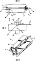
Fig. 1 is the side view of optical structure element according to an embodiment of the invention;
Fig. 2 is an isometric views of crossing irradiation changed course part according to an embodiment of the invention;
Fig. 3 is the top view of optical structure element according to an embodiment of the invention;
Fig. 4 is the front view of optical structure element according to an embodiment of the invention; With
Fig. 5 is the isometric views of optical structure element according to an embodiment of the invention.
The present invention can carry out various improvement and adopt alternative form, and certain embodiments shows by way of example in the accompanying drawings, will describe in detail below.But, should be understood that the present invention is not limited to particular forms disclosed.And, under the situation of the spirit and scope of the present invention that do not break away from the claims qualification, the present invention includes all improvement, equivalent and alternative.
Embodiment
Be used for the fluid optical detection of goals of medicine, the transmission spectrophotometric method glucose concentration determination of blood or interstitial fluid for example, can reduce the complicacy of desired medical apparatus or can be the user provides simpler instrument of operation and technology to have very big value.With reference to figure 1, the optical structure element 10 that shows among the figure can greatly reduce the complicacy of optical testing instrument design, can also make test be more prone to carry out.Optical structure element 10 comprises the irradiation input field 12 of the light beam that can receive light source 14.Light source can be a laser instrument, as diode laser, or any other types light source that is used for the medical fluid analysis.According to one embodiment of present invention, collimation input beam 16 is used for shining input field 12.According to an embodiment, input beam 16 has and is approximately 1.0 square millimeters sectional area.Light beam does not preferably exceed irradiation input field 12, but exceeds irradiation photoconduction 18.According to an embodiment of optical structure element 10, irradiation input field 12 has and is approximately 1.5 square millimeters sectional area, and irradiation photoconduction 18 has about 0.5 square millimeter sectional area.
When utilization structure spare 10, the direction guiding that irradiation photoconduction 18 shows along arrow A is from the light of irradiation input field 12.Be directed to irradiation changed course part 20 from irradiation input field 12 with input beam 16, wherein irradiation changed course part is used to make the light of irradiation to change direction, leaves the direction of light by irradiation photoconduction 18.Show that as Fig. 2 is clear according to one embodiment of present invention, irradiation changed course part 20 comprises that the first, second, third and the 4th crosses irradiation redirecting surfaces 22,24,26 and 28.Unnecessary mistake irradiation light can influence the reading accuracy of sample, therefore will guide it to leave optical structure element 10.Cross irradiation redirecting surfaces 22,24,26 and 28 and reflect input light, make the part of crossing irradiation of input irradiates light change direction, make it nearly orthogonal in irradiation photoconduction 18 by total internal reflection.According to one embodiment of present invention, the illumination beam of aiming at the input end of irradiation photoconduction 18 16 can change in ± 25 millimeters scopes, and can not owe irradiation irradiation photoconduction 18.
Fig. 2 had shown according to an embodiment of the invention irradiation changed course part, and it has four and crosses the irradiation redirecting surfaces.Each crosses irradiation redirecting surfaces position can make it to leave the irradiation photoconduction with crossing irradiation light change direction, and certain mistake is shone redirecting surfaces can make irradiation light change direction from the respective regions of crossing illumination beam.In embodiment illustrated in fig. 2, first shines redirecting surfaces 22 excessively can make the mistake irradiation light break-in at input beam 16 tops leave irradiation photoconduction 18.In this embodiment, first cross and to shine redirecting surfaces 22 and can change direction the right crossing the top (upper and lower, left and right side is by watching Fig. 2 to determine direction) of irradiation light from input beam to input beam 16 moving directions.It is contemplated that first cross shine redirecting surfaces 22 can also with cross irradiation light from the top break-in of input beam 16 to other directions.Fig. 2 has shown that second crosses irradiation redirecting surfaces 24, and the right side of irradiation light from the left side break-in of input beam 16 to input beam 16 moving directions can will be crossed in its position.What show in Fig. 2 the 3rd crosses and to shine redirecting surfaces 26 and can will cross the left side of irradiation light from the right side break-in of input beam 16 to input beam 16 moving directions.What show among Fig. 2 the 4th crosses and to shine redirecting surfaces 28 positions and can will cross the right side of irradiation light from the bottom side break-in of input beam 16 to input beam 16 moving directions.Can consider that but each is crossed irradiation redirecting surfaces 22,24,26,28 was arranged to the irradiation light break-in to other directions, comprise the upper and lower side of input direction, leave rather than by input beam, these depend on the certain applications of optical structure element 10.Can more redirecting surfaces be set or less redirecting surfaces is set according to the requirement of the embodiment of specific optical structure element.Any irradiation redirecting surfaces of crossing can be used for a part of input beam 16 change directions are become reference beam.As the following discussion of carrying out with reference to figure 3, according to one embodiment of present invention, the 4th crosses irradiation redirecting surfaces reflection reference beam.
Input irradiation redirecting surfaces 30 is reflected into irradiating light beam in the direction of arrow B by total internal reflection.According to one embodiment of present invention, irradiation redirecting surfaces 30 coateds have reflecting material.According to one embodiment of present invention, irradiation redirecting surfaces 30 is set to 18 one-tenth 45 degree of relative exposure photoconduction.
According to embodiment shown in Figure 1, after 30 reflections of input irradiation redirecting surfaces, input beam is conducted through the readout window 32 that is provided with fluid sample.Lead beam arrives samples 34 by structural member 10, makes it possible to analyze with less sample size, and provides more easily mode to gather very small amount of sample.According to an embodiment of optical structure element 10, sample 34 is directed to readout window 32 by pin 36 or kapillary.Pin 36 can be opened patient and collected specimens by an action thorn.Ci Kai and collected specimens combination have greatly been simplified the operation that the patient is carried out.Readout window 32 is as optically transparent platform, and the fluid sample of testing on it is relative exposure photoconduction 18 and irradiation redirecting surfaces 30 location accurately.According to one embodiment of present invention, reagent is in readout window 32 desiccation.In this embodiment, reagent and sample are recombinated, and make sample change color occur.
According to one embodiment of present invention, the optics that input beam passes through is read the district and has been in harmonious proportion the defective of readout window 32 through optimizing, and has been in harmonious proportion the inhomogeneous colour developing of sample, has improved the signal level of signal detector.Light beam after interacting between readout window 32 and the sample 34 can be described as the detection light beam.
After sample 34 interactions, detect light beam and enter detection photoconduction 40 along direction shown in the arrow C by detecting redirecting surfaces 38 break-ins.According to one embodiment of present invention, detect the redirecting surfaces 38 relative photoconductions 40 that detect and be arranged to 45 degree.But detect redirecting surfaces 38 coated reflecting materials.Detect photoconduction 40 guiding and detect light beam, output to detecting device 44 then to detecting output terminal 42.According to one embodiment of present invention, light source 14 and detecting device 44 are installed in the inside of instrument, and optical structure element 10 is positioned at the outside of instrument.In this embodiment, sample collecting is easy to realize, and can be seen by patient.Sample remains on the outside of instrument and can not pollute the optical device of instrument or instrument.
In optical structure element 10 of the present invention, irradiation photoconduction 18, readout window 32 and the aligning that detects between the photoconduction 40 are fixed, because these elements are parts of optical structure element 10.According to one embodiment of present invention, the cross section of the sectional area ratio irradiation photoconduction 18 of detection photoconduction 40 is wide, allows not to be that the light beam that collimates fully can be directed to detecting device 44.Therefore, the optical structure element that comprises light path or waveguide makes sample that uniform beam propagation be arranged when carrying out optic test and consistent reading is arranged.
Continuation has shown the top view according to optical structure element 10 of the present invention with reference to figure 3 among the figure.Except the parts of introducing above, Fig. 3 shown make that reference beam 46 changes directions cross irradiation redirecting surfaces 28, be used for comparing with light beam by sample.Reference beam detects by reference detector 48, can correct by carrying out sample reading and datum readings simultaneously because the signal that light source or thermal gradient instability cause changes.The comparison of sample signal and reference signal can be eliminated and not be that the signal that is caused by sample 34 changes.
Fig. 4 has shown the front view according to optical structure element 10 of the present invention.Shown reference beam 46 among the figure with irradiation photoconduction 18 and the axis quadrature that detects photoconduction 40.Fig. 5 has shown the isometric views of optical structure element 10 according to an embodiment of the invention.
Use waveguide optical structural member 10 of the present invention, allow about 0.75 millimeter best optics and read diameter, and can between structural member and optical device, increase the machine error of necessity of ± 0.500 millimeter.In addition, adopt the molded optical structure element of optical clear plastics greatly to reduce complicacy and the cost of making optical structure element.Although the size of optical structure element 10 of the present invention can be amplified in proportion or dwindles according to specific application scenario, according to an embodiment, the cross section of irradiation photoconduction 14 is approximately 0.50 square millimeter.For such area, before irradiation photoconduction 14 was full of by the light less than acceptable number, nearly ± 0.5 millimeter of alignment point can be departed from the position of input beam or optical structure element 10.Optical element is set to the consistance that can strengthen the optical sample reading in the structural member greatly, especially when using a small amount of sample.
Though with reference to one or more specific embodiments the present invention is introduced, the professional and technical personnel in affiliated field will be appreciated that under the situation that does not break away from the spirit and scope of the present invention can carry out many changes.For example, though the present invention relates generally to medical application, will be appreciated that any optical fluid Test Application can adopt principle of the present invention.Will be appreciated that each embodiment and change all should belong in the spirit and scope of the present invention that scope of the present invention is limited by claims.
Claims (20)
1. structural member that sample is carried out optical analysis comprises:
The irradiation input field;
The irradiation photoconduction is communicated with described irradiation input field light and forms input light path;
Readout window is with described input light path quadrature roughly;
Detect photoconduction, be arranged to approximate parallelly with described input light path, the nearly described readout window of a termination, the other end form and detect output terminal; With
One or more irradiation redirecting surfaces of crossing can make the turn light rays of the described irradiation photoconduction of irradiation leave described irradiation photoconduction.
2. structural member according to claim 1, it is characterized in that, described irradiation photoconduction, described readout window and described detection photoconduction constitute light path, and described structural member also comprises at described irradiation photoconduction on the described light path and the irradiation redirecting surfaces between the described readout window.
3. structural member according to claim 1, it is characterized in that, described irradiation photoconduction, described readout window and described detection photoconduction constitute light path, and described structural member also comprises the detection redirecting surfaces between described readout window on the described light path and described detection photoconduction.
4. structural member according to claim 1 is characterized in that, described structural member also comprises from the outward extending pin of described readout window, is used for sample is placed into described readout window.
5. structural member according to claim 1 is characterized in that described structural member also is included in the dried reagent of described readout window.
6. structural member according to claim 1 is characterized in that, described irradiation photoconduction has the irradiation section of light guide, and described detection photoconduction has the detection section of light guide greater than described irradiation section of light guide.
7. structural member according to claim 1 is characterized in that, described irradiation photoconduction and described detection photoconduction are the monomer spares that is molded as by optically transparent material.
8. structural member according to claim 1 is characterized in that, described irradiation photoconduction and described detection photoconduction are the individual components that is molded as by optically transparent material, are connected in the single optical structure element.
9. structural member according to claim 1 is characterized in that, described one or more mistakes are shone light nearly orthogonal that the bootable mistake of redirecting surfaces shines described irradiation photoconduction in described irradiation photoconduction.
10. structural member according to claim 1 is characterized in that, 4 described irradiation redirecting surfaces are excessively arranged, and each described irradiation redirecting surfaces excessively and described irradiation photoconduction form about miter angle.
11. a molded waveguide optical structural member comprises:
The irradiation input field;
The irradiation photoconduction can receive the light from described irradiation input field;
The first, second, third and the 4th crosses the irradiation redirecting surfaces, is arranged to become about 45 degree with described irradiation input field, and the bootable irradiates light of crossing leaves described irradiation photoconduction;
Input irradiation redirecting surfaces is positioned at described irradiation photoconduction to become on the plane of about miter angle;
Detect redirecting surfaces, be positioned at described mistake and shine on the plane of redirecting surfaces nearly orthogonal;
Readout window is arranged between described irradiation redirecting surfaces and the described detection redirecting surfaces, can receive the light on the direction that roughly is orthogonal to described irradiation photoconduction;
Detect photoconduction, be roughly parallel to described irradiation photoconduction and be communicated with described detection redirecting surfaces light; With
Detect output terminal, exportable light from described detection photoconduction.
12. molded waveguide optical structure element according to claim 11 is characterized in that, described irradiation photoconduction has about 0.50 square millimeter irradiation photoconduction sectional area, and described detection photoconduction has greater than 0.80 square millimeter detection section of light guide long-pending.
13. the method that sample is carried out optical analysis may further comprise the steps:
Collected specimens is put into optical waveguide structure spare;
Guiding light is directed to irradiation photoconduction with light from described irradiation input field to the irradiation input field of described structural member;
Make the light of the described irradiation photoconduction of irradiation change direction, left described irradiation photoconduction;
The described light of optical guidance is by described structural member and described sample; With
Detection is from the light of the detection output terminal of described structural member.
14. method according to claim 13 is characterized in that, makes the step of the light change direction of the described irradiation photoconduction of irradiation also comprise the formation reference beam.
15. method according to claim 13 is characterized in that, the step that light is directed to the irradiation input field of described structural member comprises the irradiation input field that makes light overflow described structural member.
16. a waveguide optical structural member that is used for the sample optic test comprises:
The input field receives the light that enters described optical structure element, and described light is advanced along input direction;
The first, second, third and the 4th crosses the irradiation redirecting surfaces, is arranged to light to be reflexed to direction approximate and described input direction quadrature from described input direction;
The irradiation photoconduction receives the light from described input field, and is arranged to and can guides described light along described input direction;
The irradiation redirecting surfaces is arranged to and light can be reflexed to direction with described input direction nearly orthogonal from described input direction;
Readout window is used for keeping sample and the light that receives from described irradiation redirecting surfaces;
Detect redirecting surfaces, be arranged to receive light from described readout window, and along the light of parallel with described input direction haply direction reflection from described readout window;
Detect photoconduction, receive light from described redirecting surfaces; With
Detect output terminal, receive from the light of described detection photoconduction and guide described light outside described optical structure element.
17. optical structure element according to claim 16 is characterized in that, described detection redirecting surfaces also can reflect described light along the direction opposite with described input direction.
18. optical structure element according to claim 16 is characterized in that, described structural member also comprises the pin that is used to obtain sample, described sample can be directed to described readout window.
19. optical structure element according to claim 16 is characterized in that, described structural member also comprises the kapillary that is used to obtain sample, described sample can be directed to described readout window.
20. optical structure element according to claim 16 is characterized in that, described readout window has about 1 millimeter diameter.
Applications Claiming Priority (2)
| Application Number | Priority Date | Filing Date | Title |
|---|---|---|---|
| US44085903P | 2003-01-21 | 2003-01-21 | |
| US60/440859 | 2003-01-21 |
Publications (1)
| Publication Number | Publication Date |
|---|---|
| CN1517696A true CN1517696A (en) | 2004-08-04 |
Family
ID=32595358
Family Applications (1)
| Application Number | Title | Priority Date | Filing Date |
|---|---|---|---|
| CNA2004100033459A Pending CN1517696A (en) | 2003-01-21 | 2004-01-20 | Small capacity moulded waveguide optical structure |
Country Status (6)
| Country | Link |
|---|---|
| US (1) | US8377381B2 (en) |
| EP (1) | EP1441214A3 (en) |
| JP (1) | JP2004245830A (en) |
| CN (1) | CN1517696A (en) |
| AU (1) | AU2004200217A1 (en) |
| CA (1) | CA2455218A1 (en) |
Cited By (1)
| Publication number | Priority date | Publication date | Assignee | Title |
|---|---|---|---|---|
| CN110095456A (en) * | 2019-04-12 | 2019-08-06 | 中国农业科学院烟草研究所(中国烟草总公司青州烟草研究所) | A kind of tobacco virus detection display and application method |
Families Citing this family (12)
| Publication number | Priority date | Publication date | Assignee | Title |
|---|---|---|---|---|
| WO2007045412A1 (en) * | 2005-10-15 | 2007-04-26 | F. Hoffmann-La Roche Ag | Test element and test system for examining a body fluid |
| US9423397B2 (en) | 2006-03-10 | 2016-08-23 | Indx Lifecare, Inc. | Waveguide-based detection system with scanning light source |
| US8288157B2 (en) * | 2007-09-12 | 2012-10-16 | Plc Diagnostics, Inc. | Waveguide-based optical scanning systems |
| US9976192B2 (en) | 2006-03-10 | 2018-05-22 | Ldip, Llc | Waveguide-based detection system with scanning light source |
| US9528939B2 (en) | 2006-03-10 | 2016-12-27 | Indx Lifecare, Inc. | Waveguide-based optical scanning systems |
| US8052618B2 (en) | 2006-10-15 | 2011-11-08 | Roche Diagnostics Operations, Inc. | Diagnostic test element and process for its production |
| WO2009046957A2 (en) * | 2007-10-08 | 2009-04-16 | Roche Diagnostics Gmbh | Analysis system for automatic skin prick analysis |
| GB2461026B (en) | 2008-06-16 | 2011-03-09 | Plc Diagnostics Inc | System and method for nucleic acids sequencing by phased synthesis |
| EP2425286B1 (en) | 2009-04-29 | 2020-06-24 | Ldip, Llc | Waveguide-based detection system with scanning light source |
| CN102271204A (en) * | 2010-06-04 | 2011-12-07 | 株式会社东芝 | Lighting device, image reading device, image forming apparatus and image reading method |
| US10018566B2 (en) | 2014-02-28 | 2018-07-10 | Ldip, Llc | Partially encapsulated waveguide based sensing chips, systems and methods of use |
| WO2016138427A1 (en) | 2015-02-27 | 2016-09-01 | Indx Lifecare, Inc. | Waveguide-based detection system with scanning light source |
Family Cites Families (17)
| Publication number | Priority date | Publication date | Assignee | Title |
|---|---|---|---|---|
| US3141094A (en) | 1960-10-27 | 1964-07-14 | Beckman Instruments Inc | Photoelectric immersion probe |
| US4803992A (en) | 1980-10-28 | 1989-02-14 | Lemelson Jerome H | Electro-optical instruments and methods for producing same |
| JPS60501622A (en) | 1983-06-11 | 1985-09-26 | グライネル・インスツルメンツ・アクチエンゲゼルシャフト | Liquid photometric analysis device |
| JPS61159121A (en) | 1984-12-29 | 1986-07-18 | Omron Tateisi Electronics Co | Electronic thermometer |
| US4710623A (en) | 1986-02-27 | 1987-12-01 | Eli Lilly And Company | Optical fiber catheter with fiber-contained reactive element |
| US4873993A (en) | 1986-07-22 | 1989-10-17 | Personal Diagnostics, Inc. | Cuvette |
| GB8619823D0 (en) | 1986-08-14 | 1986-09-24 | Buckley B M | Determining level of analyte |
| US4818263A (en) | 1987-06-11 | 1989-04-04 | Tektronix, Inc. | Method and apparatus for precisely positioning microlenses on optical fibers |
| DK163194C (en) | 1988-12-22 | 1992-06-22 | Radiometer As | METHOD OF PHOTOMETRIC IN VITRO DETERMINING A BLOOD GAS PARAMETER IN A BLOOD TEST |
| US5418615A (en) | 1994-02-25 | 1995-05-23 | Axiom Analytical, Inc. | Probe for liquid sample analysis by light transmission |
| DE69637553D1 (en) | 1995-12-19 | 2008-07-10 | Abbott Lab | Device for detecting an analyte and administering a therapeutic substance |
| US6001307A (en) | 1996-04-26 | 1999-12-14 | Kyoto Daiichi Kagaku Co., Ltd. | Device for analyzing a sample |
| JPH09308624A (en) | 1996-05-23 | 1997-12-02 | Minolta Co Ltd | Attachment for concentration measuring instrument and concentration measuring system |
| US6216022B1 (en) * | 2000-06-22 | 2001-04-10 | Biosafe Laboratories, Inc. | Implantable optical measurement device and method for using same |
| BR0016711A (en) | 1999-12-24 | 2002-09-03 | Roche Diagnostics Gmbh | Test Element Analysis System |
| US6620112B2 (en) | 2000-03-24 | 2003-09-16 | Novo Nordisk A/S | Disposable lancet combined with a reagent carrying strip and a system for extracting and analyzing blood in the body utilizing such a disposable lancet |
| CA2446328C (en) | 2002-10-29 | 2013-12-31 | Bayer Healthcare Llc | Optical reagent format for small sample volumes |
-
2004
- 2004-01-02 US US10/750,271 patent/US8377381B2/en active Active
- 2004-01-15 CA CA002455218A patent/CA2455218A1/en not_active Abandoned
- 2004-01-15 EP EP04000699A patent/EP1441214A3/en not_active Withdrawn
- 2004-01-19 AU AU2004200217A patent/AU2004200217A1/en not_active Abandoned
- 2004-01-20 JP JP2004011735A patent/JP2004245830A/en active Pending
- 2004-01-20 CN CNA2004100033459A patent/CN1517696A/en active Pending
Cited By (2)
| Publication number | Priority date | Publication date | Assignee | Title |
|---|---|---|---|---|
| CN110095456A (en) * | 2019-04-12 | 2019-08-06 | 中国农业科学院烟草研究所(中国烟草总公司青州烟草研究所) | A kind of tobacco virus detection display and application method |
| CN110095456B (en) * | 2019-04-12 | 2021-08-20 | 中国农业科学院烟草研究所(中国烟草总公司青州烟草研究所) | Tobacco virus detection and development device and use method |
Also Published As
| Publication number | Publication date |
|---|---|
| EP1441214A2 (en) | 2004-07-28 |
| AU2004200217A1 (en) | 2004-08-05 |
| CA2455218A1 (en) | 2004-07-21 |
| JP2004245830A (en) | 2004-09-02 |
| US20040142370A1 (en) | 2004-07-22 |
| US8377381B2 (en) | 2013-02-19 |
| EP1441214A3 (en) | 2005-01-12 |
Similar Documents
| Publication | Publication Date | Title |
|---|---|---|
| CN1517696A (en) | Small capacity moulded waveguide optical structure | |
| CA1321487C (en) | Readhead for reflectance measurement of distant samples | |
| US5359184A (en) | Optical encoding utilizing selectively refracted light | |
| US11035784B2 (en) | Methods and systems for optical hemoglobin measurement | |
| EP1882916A1 (en) | Compact catadioptric spectrometer | |
| RU2519505C2 (en) | Sensor device for target substance identification | |
| US20040241736A1 (en) | Analyte determinations | |
| JPH11258150A (en) | Medical diagnosis apparatus using fresnel reflecting body | |
| US6522398B2 (en) | Apparatus for measuring hematocrit | |
| US20030133840A1 (en) | Segmented area detector for biodrive and methods relating thereto | |
| JP6524305B2 (en) | Apparatus and method for determining blood settling velocity and other parameters associated therewith | |
| JP3919749B2 (en) | Configuration and method of optical apparatus for differential refractive index measurement | |
| US7964412B2 (en) | Optical reagent format for small sample volumes | |
| EP3892982A1 (en) | Cartridge for spectroscopic device for quantification in biological fluids, respective kit and method of use thereof | |
| JP4696934B2 (en) | Analysis equipment | |
| CN206920451U (en) | A kind of test strips for detecting glycosylated hemoglobin | |
| US20210088534A1 (en) | Joint hematology and biochemistry point-of-care testing system | |
| JP2010521679A (en) | Biosensor cartridge and biosensor mounting system in which fluid storage mechanism and fluid selection mechanism are integrated | |
| AU726717B2 (en) | Improved analyzer throughput featuring through-the-tip-analysis | |
| US20230003722A1 (en) | Methods and compositions for lateral flow analyte assays | |
| KR20230096960A (en) | Light source for variable path length systems | |
| CN1237705A (en) | Biomolecular interaction real-time phase detection analysis method and its system | |
| CN1546990A (en) | Photodetector on micro biochemical chip | |
| EP4267941A1 (en) | Porous unit without reflective layer for optical analyte measurements | |
| CN104359872A (en) | Device for measuring wavelength transmittance |
Legal Events
| Date | Code | Title | Description |
|---|---|---|---|
| C06 | Publication | ||
| PB01 | Publication | ||
| C10 | Entry into substantive examination | ||
| SE01 | Entry into force of request for substantive examination | ||
| C02 | Deemed withdrawal of patent application after publication (patent law 2001) | ||
| WD01 | Invention patent application deemed withdrawn after publication |