CN1511332A - Device and method ofr examination of samples in non-vacuum environment using scanning electron microscope - Google Patents
Device and method ofr examination of samples in non-vacuum environment using scanning electron microscope Download PDFInfo
- Publication number
- CN1511332A CN1511332A CNA018199062A CN01819906A CN1511332A CN 1511332 A CN1511332 A CN 1511332A CN A018199062 A CNA018199062 A CN A018199062A CN 01819906 A CN01819906 A CN 01819906A CN 1511332 A CN1511332 A CN 1511332A
- Authority
- CN
- China
- Prior art keywords
- chamber
- barrier film
- sample
- electron
- cell
- Prior art date
- Legal status (The legal status is an assumption and is not a legal conclusion. Google has not performed a legal analysis and makes no representation as to the accuracy of the status listed.)
- Pending
Links
Images


Classifications
-
- H—ELECTRICITY
- H01—ELECTRIC ELEMENTS
- H01J—ELECTRIC DISCHARGE TUBES OR DISCHARGE LAMPS
- H01J37/00—Discharge tubes with provision for introducing objects or material to be exposed to the discharge, e.g. for the purpose of examination or processing thereof
- H01J37/26—Electron or ion microscopes; Electron or ion diffraction tubes
- H01J37/28—Electron or ion microscopes; Electron or ion diffraction tubes with scanning beams
-
- H—ELECTRICITY
- H01—ELECTRIC ELEMENTS
- H01J—ELECTRIC DISCHARGE TUBES OR DISCHARGE LAMPS
- H01J37/00—Discharge tubes with provision for introducing objects or material to be exposed to the discharge, e.g. for the purpose of examination or processing thereof
- H01J37/02—Details
- H01J37/20—Means for supporting or positioning the objects or the material; Means for adjusting diaphragms or lenses associated with the support
-
- H—ELECTRICITY
- H01—ELECTRIC ELEMENTS
- H01J—ELECTRIC DISCHARGE TUBES OR DISCHARGE LAMPS
- H01J2237/00—Discharge tubes exposing object to beam, e.g. for analysis treatment, etching, imaging
- H01J2237/006—Details of gas supplies, e.g. in an ion source, to a beam line, to a specimen or to a workpiece
-
- H—ELECTRICITY
- H01—ELECTRIC ELEMENTS
- H01J—ELECTRIC DISCHARGE TUBES OR DISCHARGE LAMPS
- H01J2237/00—Discharge tubes exposing object to beam, e.g. for analysis treatment, etching, imaging
- H01J2237/20—Positioning, supporting, modifying or maintaining the physical state of objects being observed or treated
- H01J2237/2002—Controlling environment of sample
- H01J2237/2003—Environmental cells
-
- H—ELECTRICITY
- H01—ELECTRIC ELEMENTS
- H01J—ELECTRIC DISCHARGE TUBES OR DISCHARGE LAMPS
- H01J2237/00—Discharge tubes exposing object to beam, e.g. for analysis treatment, etching, imaging
- H01J2237/26—Electron or ion microscopes
- H01J2237/28—Scanning microscopes
- H01J2237/2803—Scanning microscopes characterised by the imaging method
- H01J2237/2807—X-rays
Abstract
A chamber (34) suitable for use with a scanning electron microscope. The chamber comprises at least one aperture sealed with a membrane (36). The membrane (36) is adapted to withstand a vacuum, and is transparent to electrons and the interior of the chamber (34) is isolated from said vacuum. The chamber is useful for allowing wet samples (32) including living cells to be viewed under an electron microscope.
Description
FIELD OF THE INVENTION
The present invention relates to a kind of apparatus and method that adopt scanning electron microscopy sample survey under non-vacuum environment, particularly but be not limited to this apparatus and method are checked object under wet environment use.
The background technology of invention
Optical microscopy is owing to optical wavelength is restricted in 100 nanometers, is generally the resolution in the hundreds of nanometer range.Scanning electron microscopy (SEM) does not have this restriction and can be implemented in the interior quite high resolution of several nanometer range.
One of shortcoming of SEM is that sample must keep in a vacuum, and this has hindered to the research of handling under field conditions (factors) or to the research of wet stock.In addition, the electric insulation sample that is made of organic material needs coating to avoid the electric charge accumulation.
As far back as nineteen sixty, the paper of Thomley (Cambridge University, nineteen sixty) discloses the failure that keeps sample to be used for electron microscope technique and has attempted under the atmospheric environment of steam.Adopt the diaphragm seal chamber to make its influence of avoiding the vacuum of electron beam, and chamber itself have the inlet from the source of steam.
The trial of adopting electron microscope technique to be used for active sample will be traced back to 1970.The article of delivering by Swift and Brown (J.Phys.E:Sci.Instrum.3,924,1970) disclose employing transmission electron microscope (TEM) be used under atmospheric pressure, for example at the built for in-water survey sample.Employing has with the container in the hole of collodion-carbon film sealing installs sample.Electron beam is through via hole and clash into sample, and electronics can not stop by sample but continue to arrive scintillator, produces photon there.Under atmospheric pressure,, find that these results are " quite noisy " though claim the resolution of 0.1 μ m.
U.S. Pat 4071766 has been introduced the trial of adopting electron microscope technique test material under non-vacuum environment, and the detection of active object is called " problem of constantly regenerating ".U.S. Pat 4720633 has been introduced the further trial of adopting electron microscope technique test material under non-vacuum environment.In these patents, electron beam passes the hole and runs on the wet sample.Yet, successfully to observe aspect the wet object, these trials all do not have successfully.Here it is for reference to quote these documents as proof.
The commercial product of attempting to address the above problem is environmental scanning electron microscope (ESEM), can buy from the Philips Electronics Optical Co., Ltd of the dust moral Hough of Holland, and it keeps the vacuum gradient along electron beam path.Yet ESEM needs the critical point work of sample at water-balance of steam state, and requires sample is cooled to about 4 ℃.It is believed that can sample survey under up to the pressure of 5 torrs.Yet, up to the present, do not have the evidence explanation can observe wet and/or active object at 10nm and following resolution.Can in U.S. Pat 5250808,5362964 and 5412211, see that it is for reference to quote its content here as proof about the further information how work this product and it.
The universal method that realizes the high-resolution check of organic substance is transmission electron microscopy (TEM).TEM requires the sample of the special preparation of common thickness in the 50nm scope.Apply extra-high voltage passes sample with generation parallel electron beam.U.S. Pat 5406087 discloses the sample holding device of a kind of TEM of being used for, and it is for reference to quote the document here as proof.Sample is sealed between two films of energy transmission electronic bundle.Fill with moisture the inside of device, and can be placed in the vacuum environment of TEM.High beam passes the sample operation and surrounds fluid, causes bad signal to noise ratio, and sample is caused sizable damage.
Usually (in Griffiths (2001) " trend of cell biology ", comment on, 11:4:153-154) can not obtain by other technology by the EM acquired information.The main cause of the general underutilization of EM is the complexity of sample preparation, and this not only needs a large amount of labours and consuming time, and relates to the biological related raising about the result.The ability of implementing EM under water environment will solve these problematic sample preparation steps.
Therefore, at present,, do not propose to allow the microscope of the wet sample of research under the resolution that shows macro molecules and details molecular level although need for a long time yet.In the same different field of cell biological and industrially need this ability in as oil, food and microelectronics with polymer science.Particularly in the cell biological field, this microscope should be able to analysis of cells and is carried out the measurement of molecular level technology, and medicine find and diagnostic measurement aspect opening a brand-new field.What for example, this microscope will allow to react between medicine and the competent cell studies in great detail and Direct observation.
Summary of the invention
The purpose of this invention is to provide and be applicable to the chamber that uses with scanning electron microscopy, it makes it possible to achieve the electron microscopy to wet sample.
According to first scheme of the present invention, provide to be applicable to the chamber that uses with scanning electron microscopy, described chamber comprises: at least one hole, this hole diaphragm seal, described barrier film is suitable for bearing vacuum, and is electron permeable, wherein said chamber and described vacuum insulation.
Preferably, chamber is suitable for keeping substantially water or any aqueous medium under atmospheric pressure, include but not limited to cell culture medium.
Preferably, has diameter in the 0.1-4mm scope by the hole of diaphragm seal.
Preferably, barrier film has the thickness in 200-5000 dust scope basically, more preferably, and in 500 and 2000 dust scopes, and most preferably in the scope between 500 and 1500.
This barrier film constitutes main element of the present invention, its needed characteristic comprises the vacuum that can bear electron microscope and is included in by the about atmospheric pressure differential between the environment in the chamber of described diaphragm seal, simultaneously it is very thin, is enough to that high energy electron is passed and interacts with the sample that is arranged in the chamber.Any material with these attributes is applicable to the use according to principle of the present invention.According to presently preferred embodiment, diaphragm material is selected from polyimides, polyamide, polyamide-imides, polyethylene, polypyrrole and additional conductive polymer, parlodion, collodion, Kapton (polyimide film), FomrVar (a series of products of polyvinyl formal and chlorine vinegar polyvinyl alcohol terpolymer), Vinylec (polyvinyl formal), ButVar (polyvinyl butyral resin), Pioloform (Pioloform, polyvinyl acetal), silicon dioxide, silicon monoxide and carbon.
Preferably, sample is placed on the place near barrier film.Perhaps, sample is placed and contacts with described barrier film, and the advantage of She Zhiing is that electron beam must pass material (relative with vacuum) arrival sample through minimum range like this.Barrier film is preferably by the support grid support that is arranged between barrier film and the vacuum.
Usually, chamber is arranged in vacuum, and sample is enclosed in the fluid or basic under the atmospheric pressure, or under the both of these case.At least a portion of the wall of described chamber can be resisted an atmospheric pressure gradient and is transparent to having the electronics that is higher than 2KeV.
According to alternative plan of the present invention, a kind of device that adopts scanning beam in chamber middle high-resolution inspected object is provided, comprise the vacuum path that is used for electron beam and be arranged to the vacuum-resistant block piece relevant that the placement of described vacuum-resistant block piece makes it isolate object and vacuum with object.Can have fluorescence and electroluminescence mark on the object, electron beam can the excitation photons emission thus.Mark can be relevant with interested specific molecular or analog, and this method is considered the image based on light that contains relevant for the information of individual molecular.This embodiment preferably includes optical detection unit, and chamber can constitute the part of photoconduction.Optical detection unit also can comprise photomultiplier.
Optical detection unit can be suitable for detecting single photon, and this device is thus suitable for detection resources luminous from the excitation of individual molecule.
In preferred embodiment, block piece or barrier film can be any in polyimides, polyamide, polyamide-imides, Kapton (polyimide film), FomrVar (polyvinyl formal) and the polyvinyl butyral resin.
Block piece or barrier film can be with placing the enhancing screen between described barrier film and the described vacuum to strengthen, and can have the thickness in 200-5000 dust scope basically, more preferably in 500 to 2000 dust scopes, and most preferably in 500 to 1500 scopes.
Preferably, block piece or barrier film are crossed a hole and are placed, and the diameter in this hole is basically in the 0.1-4mm scope.In particularly preferred embodiment, this diameter is essentially 1mm.
The preferred transmissive high energy electron of block piece or barrier film just is meant the electronics that has above the energy of 2keV or 3keV.
According to an embodiment, apply block piece with layer of material, this material has high secondary electron production, is generally lithium fluoride.
In one embodiment, atomic group scavenger molecule is positioned at the position that is associated with described object.
In one embodiment, object or sample are placed on place adjacent with described vacuum-resistant block piece or that be in contact with it.
According to third party's case of the present invention, a kind of application of barrier film is provided, the exposed area that wherein has the 1mm diameter can be resisted an atmospheric pressure gradient, and this barrier film transmissive high energy electron, thereby constitute a chamber, can under scanning beam, observe wet sample with the resolution that is better than 100nm basically.
According to cubic case of the present invention, a kind of method of observing wet object in nanometer range resolution is provided, may further comprise the steps:, isolate the wet object in the described chamber by adopting block piece separate chambers and vacuum chamber; Provide electron beam to clash into described sample from described vacuum chamber by described block piece; With observe the secondary that penetrates from described chamber and at least one of back scattered electron.
Preferably, block piece comprises barrier film, and it is selected bearing atmospheric pressure basically, and has the electron permeable above 2keV left and right sides energy.
Preferably, wet object comprises drug ingedient.
Preferably, wet object also comprises and the interactional competent cell of described drug ingedient.
Preferably, described chamber comprises fluid intake, and wherein drug ingedient is with respect to dynamically being changed by the concentration or the type of inlet at viewing duration.
Brief description of drawings
In order to understand the present invention better and to show how the present invention effectively implements, and describes by example below with reference to accompanying drawing, wherein:
Fig. 1 is the general schematic view of longitudinal cross-section of the sample area of expression prior art scanning electron microscopy.
Fig. 2 is that expression comprises the general schematic view according to the longitudinal cross-section of the scanning electron microscopy of the chamber of the embodiment of the invention.
Fig. 3 is the summary schematic cross-section of chamber according to an embodiment of the invention.
Fig. 4 is the summary schematic cross-section that is embedded in the chamber according to another embodiment of the present invention in the photoconduction.
Fig. 5 is the electron micrograph that the embodiment of employing Fig. 3 obtains.
Fig. 6 is the schematic diagram that is used for the assembling sample chamber unit of fluorescence.
Fig. 7 A-E is the schematic diagram of components A-E of the chamber of Fig. 6.
Fig. 8 is the schematic diagram that is used for the microscope level adapter that uses with chamber.
Fig. 9 is the schematic diagram that is used for luminous alternative embodiment.
Figure 10 is illustrated in the image of the fixedly wet cell below the separation membrane.
Figure 11 is illustrated in the image of the active unmarked adherent cell below the barrier film.
Figure 12 is the image of the complete unlabelled Chinese hamster ovary celI below barrier film.
Figure 13 is the activity image of adherent cell not below the barrier film.
Figure 14 is the cathodoluminescence image of fix N H3T3 cell.
Figure 15 is the image of complete NH3T3 cell.
Detailed description of the invention
The invention provides a kind of new technology that is suitable for studying the SEM of wet sample. Wet environment is arranged in the capacitor by diaphragm seals, its septation enough thin in case high energy electron can pass and with just interact at studied sample.
We are open technology and mechanism by barrier film signal formation during to the sample imaging in SEM now in detail. We are also open as the needed machinery of the barrier film of the main element in the method and spatial placement and performance.
We disclose the simple measurement about the feature of barrier film, and the guide of selection material and thickness is provided. We also disclose the performance of this technology to various different imaging of samples. We have assessed contrast and the resolution ratio of easy realization and have obtained this contrast and the required process of resolution ratio. We show and can observe gold grain in water with the resolution ratio of the 10nm order of magnitude, and the quite low resolution ratio of the 100nm order of magnitude can be provided than the low contrast material. This new technology can be suitable for the various application in the different field, such as investigation of materials and cell biology.
The present invention is based on by introducing membranaceous separator and make fluid sample and vacuum insulation. The recent development of polymer technology be so that can make the in fact film of transmissive high energy electron, and has toughness and be enough to bear atmospheric pressure on a side and the high vacuum on opposite side. It is inner that the volume of imaging is positioned at the position of the most close barrier film, is generally the position that enters a few μ m in the fluid. This is for being positioned on the membrane surface or being desirable near the check of the object (as adhering to biological cell) of barrier film. Technology disclosed herein also is suitable for all existing SEM easily, can at room temperature with under the atmospheric pressure measure.
A, experiment arrange
We have successfully adopted apparatus and method of the present invention to carry out work with JEOL 6400 SEM and Philips ESEM under the high vacuum pattern, but the device that we propose can use with any SEM. Describe below with reference to accompanying drawings some present preferred embodiment of the present invention in detail.
Sample is contained in chamber interior, and this chamber is the line design that plug is installed along standard SEM sample. Main emphasis is the sample sealing poor with respect to external pressure, and this is realized by a series of O shape rings. There is the risk of damage barrier film in the sealing sample, because if attempt fluid in the compression chamber owing to we suitably seal the someone with barrier film with sample, will cause sizable distortion. For avoiding this problem, little release groove stays open by the handle of plug, a small amount of release balance by fluid internal pressure. The opening that led to afterwards this groove with another O shape ring sealing that suitably screws.
This barrier film must have several key properties. The first, must be electron permeable as much as possible. This is hinting harmonic(-)mean atomicity (low Z) and low-density. Therefore polymer film is only selection.
This barrier film also needs extraordinary mechanical performance. Thickness is as far as possible little in order to make the minimized while of the scattering of electronics before they arrive interested zone keeping, and barrier film must can be resisted an atmospheric pressure differential in the surf zone that may need for observation station. It also must have enough pliabilities, can carry out the processing of a great deal of in preparation during sample, controls our carbon film, because a little less than they are highly brittle. The porosity that comprises sample fixer and be positioned at the material of sample interior must reduce to guarantee the appropriate seal of chamber as far as possible.
Ideally, the electric conductivity of barrier film very your pupil is charged with the outer surface part that prevents barrier film, and this may hinder incident beam and make image blurring unclear. In fact, we make the thin carbon film dehydration on the barrier film outside, have therefore eliminated charged effect.
At last, barrier film may be very important factor to the affinity of observed object. Usually in electron microscope, electronics advances to the bottom from upper area, so the object that we will observe is positioned at below the barrier film. In the method for research, when the closely close barrier film of object, obtain best result, and best when object is fixed on the barrier film.
After tested different material to consist of barrier film, all material is all take carbon compound as the basis. After tested general in to consist of support membrane [Davison and Colquhoun, J. electron microscope technique 2,35,1985 in TEM; Handley and Olsen, submicroscopic technology 4,479,1979] Formvar and Butvar and polyimides. In the middle of the test material of these marked with dates, only have last to finish all machineries of full up foot and seal request. According to a presently preferred embodiment, the Kapton of the 1450 ' thickness that is provided by Moxtex company is provided for we. This Kapton presents immeasurablel porosity to water: before in inserting SEM, sample is placed on about 10-7In the vacuum of bar several hours, and there is not detectable loss. They can be resisted at 1mm2The power that is produced by atmospheric pressure in the above window. For this power on the barrier film and risk of rupture are afterwards minimized, usually adopt the TEM Ni screen (adopting the grid of 125-330 μ m) that is fixed on the barrier film outside to reduce this surface. For electric conductivity, find that on the outer surface 50 ' carbon deposition is just enough. If necessary, realize the affinity performance by inner surface treatment.
The mechanism of B, contrast moulding
To forming signal at detector two different contributions are arranged. The firstth, the source of even noise, second comprises signal:
1, when electron beam bump barrier film, produces back scattered electron (BSE) and secondary electron (SE) by barrier film itself. The SE that only in initial several nanometers, produces (mean free path of secondary electron) can overflow from barrier film [people such as Goldstein, SEM and X ray micro-analysis, the 113rd page, Plenum press, New York, London, 1992]. Their mean free path is about about 1nm in conductor (thin carbon layer), and is within the 10nm in insulator (such as polyimides and the fluid beyond it). In barrier film and carbon coating shielding part, all produce SE.
Therefore we are owing to barrier film is realized first of signal is contributed, and it is made of BSE and SE. This contribution is uniformly, because the composition of the barrier film that we use is all identical anywhere with thickness. Hereinafter, subscript ' m ' (being used for barrier film) will represent this contribution.
2, not backscattered portions of electronics from electron beam strikes on the sample when passing barrier film. Again produce secondary electron and back scattered electron.
Here the SE that produces has no chance to overflow, and they will be stopped by barrier film (insulator) or thin carbon coating shielding part (conductor). On the contrary, the BSE that produces in sample might withdraw from backward by barrier film. When they passed barrier film, they may produce secondary electron, if produce secondary electron, and apart from the mean free path of surperficial distance less than them, then these secondary electrons can be escaped to detector.
Therefore, because the backscattering event in area-of-interest, we realize this second contribution for signal, and these events all affect SE and BSE detector. Hereinafter, subscript ' s ' (for sample) will represent this contribution.
The second contribution obviously is the interested contributions of people. It carries our conceivable information, and the first contribution only relates to barrier film (m). If the difference of the sample signal between two consecutive points is higher than the fluctuation in the diaphragm signal, then can be observed the contrast between these two consecutive points.
Therefore determine that by the probability that obtains large signal to noise ratio we form the ability of image. This is determined by the difference (" material contrast degree ") of the backscattering coefficient of the material that is positioned at sample interior again, and also depends on barrier film.
Given two kinds of different materials (its backscattering coefficient is known) also are used for special barrier film, and we will determine the condition that we must be realized in order to form image.
The resultant signal S that collects is made of secondary electron and back scattered electron:
S~ε
BSη+ε
SEδ?????(1)
With δ be respectively the ratio of BSE and SE electric current and electron beam current.Coefficient ε is the collection efficiency of two kinds of electronics being detected.
Backscattering coefficient η is made of two contributions on it: from the BSE of barrier film (m) inside with from the inner BSE of sample (s), η=η m+ η s.
Equally, SE scattering coefficient δ has two contributions: δ=δ m+ η s Δ m.
Difference is to represent secondary electron by the beam electron production that enters barrier film at δ m, when Δ m is illustrated in the secondary electron that is produced in barrier film by electronics on the outside path of electronics, and the difference after the relevant reverse scattering events of sample interior.
Therefore backscattering coefficient η s multiply by Δ m, reduces η s because the flux of the high-power electron beam of barrier film is passed in negative line feed from 1.
Notice that δ m and Δ m have described because near the Secondary Emission on the surface of barrier film.For δ m, the high energy electron that produces Secondary Emission is the major part of incident beam, and is very little from the contribution that has obtained at the inner backscattered electronics of barrier film.For Δ m, the electron beam that produces Secondary Emission has experienced the backscattering incident in sample.For this reason, Δ m can contain slow material correlation.According to the material that is positioned at below the barrier film, the power spectrum of the BSE in this zone can be different, and the different-energy of BSE may produce different SE emissions.
Definition and the common in the literature described coefficient of noting backscattering that we use and quadratic coefficients are slightly different.The latter can not be used for the semo-infinite medium, and is the characteristic of material (gold, carbon, nylon etc.).Here, coefficient is described the electric charge emission of the barrier film with its specific thicknesses and its carbon shielding part.They do not describe the electric charge emission of the semo-infinite material of polyimide material.By same mode, the sample coefficient has been described from sample interior but the signal of the material that covered by barrier film.One of our purpose will make measurement coefficient relevant with the traditional theory coefficient feature of material (for example water, gold etc.) itself by experiment in the following description.
Let us considers to provide two consecutive points of signal SA and SB.Material contrast between them is defined as follows:
C
AB=(S
A-S
B)/S
A?????(2)
(suppose S
A>S
B).
There are two basic modes to revise signal S.A kind of mode is with its multiplication by constants (amplification).Another kind of mode is to add the constant (i.e. " black level ") of plus or minus to signal.Barrier film is all identical in each place to the contribution of this signal.Its thickness and its composition are very good to be determined.Therefore can composition comparative and landform comparative not appear because of barrier film between an A and B.
Therefore contributing m is a constant, and it can be removed by suitable selection black level.Notice that although the noise of pn order of magnitude possibility interferometry, wherein n is the electron number from the barrier film scattering, we have ignored it at that time, get back to it below.By this selection, the contrast between some A and the B has just been simplified greatly:
C
AB=(ηS
A-ηS
B)/ηS
A??????(3)
The material contrast only difference of the quantity of the backscattering incident that takes place of the material below occurring in the barrier film that is arranged on an A and the B is relevant.
Get back to contribution m, its produces the noise may destroy image fully, if it has the order of magnitude of the amplitude of the signal that the incident by sample interior produces.For this reason, we must study the barrier film characteristic and quantize only to relate to barrier film and pass through suitably to select black level repressed part signal in the expression formula (equation 3) of comparative.
C, electronics pass the passage of barrier film
We continue to quantize the contribution of barrier film to signal now experimentally.For this reason we according to change with energy, study from the BSE and the SE of its surface emitting.The method that we adopt is to measure the total current of passing sample at diverse location, subtracts each other the loss that obtains in BSE and SE.We have no to measure whole electric currents that electric current provides in sample with estimation SEM with hindering, and measuring diaphragm is to the influence of this electric current then.At last, we measure by barrier film and arrive the electric current of given material, and given material is Jin Heshui under our situation.
For this reason, we adopt four different samples and allow different samples to insert the assembly (in four samples that we have, three can be inserted together, so we carry out repeated experiments with overlapping triplets and the same terms) of microscope inside simultaneously.For different energy, electron beam successfully is positioned on each sample, and has measured the electric current between ground and the sample.
Sample 1 is exactly Faraday cup [people such as Goldstein, scanning electron microscopy and X-ray microanalysis instrument, the 65th page, Plenum press, New York, London, 1992], be used for measuring line I by the electric charge (oppositely the amount of the electric charge of overflowing can be ignored) of collecting all beams
BeamIt is to be made of the carbon piece that is connected to ground, and at its top chamber (diameter of 2mm, 3mm is dark) is arranged, and is the nickel plate sealing in the hole of 10_m by diameter is arranged in the centre.Beam enters and clashes into the bottom in carbon chamber by this hole, thus main beam and in fact all scattered electrons be collected.
Sample 2 is identical in design, except the hole covers with barrier film.We claim that this measurement result is I
Barrier film
The difference between current of go up measuring at sample 1 and 2 (by sample 1 standardization) provide by with the percentage of the interaction electrons emitted of barrier film.This has measured the contribution of the secondary and the backscattering coefficient of barrier film:
[(I
Beam-I
Barrier film)/I
Beam]=η
m+ δ
m:
Beam current (sample 1) and the difference between the electric current of measuring on sample 3 or 4 provide from arriving the percentage of outside sample electrons emitted.These comprise and barrier film and all synergistic electronics of material (being respectively gold or water):
[(I
Beam-I
Barrier film+material)/I
Beam]=(η
m+ δ
m)+η
s(l+ Δ m);
Subscript S represents material, is gold or water here.
For the energy that is lower than 5keV, can see that gold and water curve are superimposed upon on the barrier film curve.The energy shortage that this means beam turns back to detector to arrive sample and to send BSE.
For the energy that is higher than 5kev, three slope of a curve differences.The growth part of detection signal is owing to cause with the material interaction of considering.Along with energy increases, this difference also increases: the material component of signal becomes major part.
For the incident electron energy of water sample and 10keV, beam-barrier film effect is 50% to the contribution of electric charge emission.Their contribution reduces to 35% when 15keV.
Under the situation of gold, because its high atomicity, this ratio is very little.When 10keV, having only 4% of emission electric charge is that barrier film is distinctive.When 15keV, the barrier film contribution drops to 2%.
In this stage, we can deduct the barrier film component from total electronics emission, and obtain the contribution of material to signal.This includes only by them and interested material and interacts and the electronics of scattering.
When low-yield, the beam electronics can not arrive sample and these curves should be zero.When very high energy, these curves should be deferred to the characteristic of the backscattering coefficient of material, and are transparent because in fact barrier film becomes.Our viewed fact on two curves that Here it is.The decline slope of water curve is deferred to the theoretical characteristics of backscattering coefficient, as derivation [Phys.Status.Soli di A56, K45,1979 according to Hunger and Kuchler; Also, p.95] calculate referring to Goldstein op cit.The slope of the growth of great hit line is also directly deferred to energy calculation backscattering coefficient assessment (as deriving from identical expression formula).
By the backscattering coefficient by each material these curves are carried out normalization (utilizing their appropriate energy correlation), we are wherein had only the curve that keeps low material correlation.
Result for water represents to hang down about 25% backscattering coefficient than the theoretical curve by Hunger and Kuchler prophesy.We can not determine what the origin of this difference is, but because our sample is closed fully, and contaminated possibility is very little, so we believe that our experiment determined value is to measure the purest available result this moment hereto.
Although we do not do direct measurement as yet to this, the performance of the material below the barrier film has also obviously influenced the power spectrum of the BSE that is launched.The scope of energy from 0 to E
0, E wherein
0It is the energy of incident electron.Light material (as carbon) has approximately with value E
0/ 2 for the center and be the symmetry distribution [Bishop in Proceedings of the 4
ThIntl.Conf.X ray light and micro-analysis are edited (Paris, 1966) by Hermann; Also can be referring to Goldstein opcit, p.100].Heavy material (as, gold) have very asymmetric BSE Energy distribution, peak value is more near E
0This difference produces two effects.The first, the ratio that can return the BSE that passes barrier film and total BSE of generation for heavy material than light material height.In fact barrier film is used to leach low energy BSE, strengthens the comparative between light element and the heavy element thus artificially.The second, BSE can also can influence SE emission Δ m by spectral difference, and this is because low energy BSE has higher possibility to produce SE on the path of penetrating at them.
For atomicity other material between water and gold, corresponding curve should shown in two limit between.We are as follows from the conclusion that above result has summed up us:
A), can not detect signal from sample for the energy below 4-keV; Can adopt thinner barrier film to reduce this threshold value.
B) zone line of energy is interesting zone, and reason is as follows: at first, barrier film has strengthened comparative between heavy material and the light material to the filtering effect of low energy BSE.Secondly, the emission of SE in this state is very important, and can utilize the SE detector to be easy to imaging.Peak value on the great hit line arrives and is higher than 1 value, the high emission of this expression SE.
C) for the energy of superelevation, the electric charge of emission is near the theoretical BSE coefficient of estimating.Reason is that the possibility of passing barrier film for BSE is higher, and the possibility of the SE on their ejaculation path is lower when higher electron energy (for two kinds of electronics of beam and back scattered electron).The Secondary Emission that relates to Δ m has reduced, and is therefore observed as experiment, by the easier imaging of BSE detector.
The membrane filtration effect of BSE is become and can ignore when the high energy.In the expression formula (equation 3) of comparative, backscattering coefficient can be replaced by the backscattering coefficient of the material of considering (water, gold, carbon etc.).The energy of realization steady section is represented least energy, and more than the least energy, this approximation is effective at this.For the barrier film shown in here, this is worth about 15keV.
D, deduction are used to observe the minimum probe current to the topping material comparative
In case between two points, have little composition poor (average atom number poor), can observe it theoretically.Problem is how a lot of electronics must strike on these aspects to observe.
This assessment is useful, has several reasons as follows.The first, selecteed current affects resolution: high electric current causes that beam-focusing is bad.This is the many-sided of problem when microscopical electron source is tungsten filament, and is insensitive problem for field emission microscope.The second, electron source can only produce the electric charge of limited quantity, and the 3rd, high radiation dose may damage sample.
Generally speaking, we are interested to be the sample that contains liquid, and as latex, biological substance, polymer solution etc., in most of the cases to be proved be low comparative sample to these materials.
Some any but useful criterion for enough observabilities is " rose criterion " [Goldstein op cit, pp215].This criterion represents that the difference of the signal amplitude between these points must be higher than 5 times of noise level in order to observe poor between two some A and the B:
(S
A-S
B)>5N。
Measurement enters the electron amount of detector when beam is in a some A with different scanning, we obtain distributing, and its standard deviation is provided by following:
~η
1/2With the center at mean value _ n.Therefore this signal and η are in direct ratio, and noise and η
1/2In direct ratio.Signal to noise ratio is S/N~η
1/2And the minimum level of observable material contrast is Cmin=5/ η
1/2
Like this, the average of the electronics that must collect in order to observe certain material comparative C is usually by η>(5/C)
2Given.Corresponding electric current (in detector) is I
s>(q/t) (5/C)
2, wherein q is an electron charge, t is the time of beam on each point.T also can be expressed as t=T/n
p, wherein T is sweep time, n
pIt is the pixel quantity of every frame.For high quality graphic, common n
p=10
6Individual pixel.Measure Is (skin ampere) and T (second), we find at detector is that the required electric current that obtains given material contrast C is:
I
s>4/TC
2????(4)
At last, signal code I
sWith beam current I
BFollowing relation is arranged:
I
s=ηs(ε
BS+ε
SEΔm)I
B。The same with the Everhart-Thornley detector, the SE detector is very effective, has the good inhibition [Goldstein opcit] to BSE.The BSE detector is not collected SE, and because it has little feature usually, therefore has only medium collection efficient.We test the energy of discovery about 10keV, and the image of BSE and SE pattern occurs with identical contrast, and the BSE pattern is better when high-energy more simultaneously.The reasonable assessment of collection efficiency is chosen as 25%, and we obtain to obtaining the needed beam current of comparative C is [19] (also at [the 217th page of Goldstein]):
I
B>16/
ηsTC
2(pA)????(5)
When high energy, comparative C is simply related to the backscattering coefficient of the material below the barrier film by equation 3.Table I represents to observe the result of calculation of the required minimum current of biological specimen such as cell, oil/water emulsion and the gold grain in water.
Four kinds of Elements C, H, N and O constitute about 99% of biological specimen (as cell) weight.Cell is made of 70% water and 29% organic compound.About 50% atom is a hydrogen atom in these compounds, the 24%th, and carbon, the 24%th, oxygen and 1% is nitrogen-atoms [20].Given these values, the average atom number of typical organic molecule is 6.72.The average atom number of water is 7.22, and the average atom number of competent cell is 7.07.Calculating at the respective opposed scattering coefficient of 20keV is 0.075 for water, and cell is 0.073.Like this, the cell that is surrounded by aqueous medium presents low comparative C=2: 5%, and backscattering coefficient is very low.This calculating shows receiving minimum current in ampere scope and is required for the typical scan of 100s.
| Material | ????Z | ????η | Comparative with water | ????I(pA) |
| Water | ????7.22 | ????0.075 | ????- | ????- |
| Cell | ????7.07 | ????0.073 | ????0.027 | ????2900 |
| Oil | ????5.8 | ????0.055 | ????0.267 | ????30 |
| Gold | ????79 | ????0.78 | ????0.90 | ????0.25 |
Table I
Observation contains the assessment of the required minimum current of the different samples of water.I calculates according to equation 3.The value of η be according to the equation of Hunger and Kuchler at the energy of E=20keV and average atom numerical value Z shown in adopting calculate.Sweep time, T=100 was typical accurately slow scanning second.
Oil/water emulsion can be more easily observed and be presented ten times of high comparative: C=26: 7%.In this case, minimum current falls into tens skins peace.For the gold grain that is immersed in the water, comparative very high (C=90%).Make its imaging only need part skin peace (table 1).
Biological sample (as cell) needs high electric current with in the reasonably imaging time of integration.People can advantageously adopt the label (as the gold grain of colloid) with heavy label to decorate cell.The latex of oil/water can directly be observed under the reference condition of the electric current and the time of integration.
When low-yield (10keV and following), it is very important that the influence of barrier film becomes.Thereby low comparative sample needs more electric current to make its imaging.
The assessment of the resolution of E, this technology
As during any electron microscope is measured, the problem of resolution finally is reduced to the existence of the scattering atom with high electron content.Do not have the strong scattering atomic time, it is very dark that beam will arrive and enter sample, standing enough interactions with before returning, with originally compared broadening and the loss resolution.In having the material of high electron density, the beam short distance of before returning or being absorbed, only advancing, so scattering volume is very little, and the resolution height.
For observing the effect of barrier film to resolution, we must assess useful signal and produce volume, it is characterized in that diameter d
Eff[Goldstein op cit., pp.162]:
d
eff=(d
2 B+d
2 m+d
2 BSE)
1/2??(6)
D wherein
BExpression enters the diameter of the beam of barrier film.Along with beam passes barrier film, produce some scattering, this is extremely important when low energy, and insignificant often when high energy.d
mRepresent to cause the broadening of beam, have zero original width d owing to the interaction of beam and barrier film
B=0 beam will be d from diameter
mBarrier film penetrate.
Apart from d
BSEBe by the average diameter of the volume of the covering of the electronics in the sample before electronics returns as BSE.d
BSECan in article [Goldstein op cit, the 105th page], find, and relate to Kanaya-Okayama (KO) scope.Change all characteristic lengths by the KO scope and remove most material correlation, only stay little atomicity Z correlation.Under the situation of golden sample, 90% of BSE begins to appear at diameter d
BSE=0.3R
KOVolume in.For carbon, identical relation provides d
BSE=0.6R
KO
The KO scope provides the typical sizes of volume of the electron interaction of material internal.It is equivalent to be the radius of the annulus at center on the surface of beam rum point, and its circumference surrounds interactional restriction and seals:
R
KO=0∶0276(A/Z)Z
0.11E0
1.67/ρ??(7)
R
KOWith um is unit, and E0 is to be the incident beam energy of unit with keV, and A is that ρ is with g/cm with the atomic weight of gram/mole expression
3The density of expression, Z is an atomicity.
(carbon barrier film-material) generally speaking theory of computation resolution at three different layers is very important.Yet under two limiting cases of the material with very low or very high atomicity, this assessment is possible.
A, the resolution of when low energy, hanging down the comparative sample
The atomicity of the material of light material Ru Shui, oil or formation barrier film is enough approaching, makes simple assessment to regard them as identical.Then, the assessment of resolution is exactly:
d
eff=(d
2 B+d
2 BSE)
1/2??(8)
D wherein
BSECalculate with average light material.As long as this assessment can detect d
BSEGet final product greater than membrane thicknesses.
The diameter d of beam
BDepend on the electron source that uses in the microscope.Field emission source (low current, high energy) under best conditions produces the 1nm beam dimension, and under hard situation, this is of a size of about 10nm.For the tungsten filament microscope, the diameter of beam can change from 10-100nm.
Like this, the resolution that obtains under the situation of light sample is in the 200nm order of magnitude.Under the situation of 10keV, low current and field emission source, provide following estimation:
d
Eff=170nm, and when 20keV, it reaches d
Eff=500nm.
By experiment, we find to be difficult to obtain than the better resolution of membrane thicknesses.When reducing energy, resolution improves, and this is because the sample volume below the barrier film diminishes.But along with energy reduces, comparative is compromise to be reduced in fact.Electronics still less is from the sample backscattering, and the ratio of sample signal and diaphragm signal reduces.Like this, the physical constraints of resolution is by detected minimum contrast providing.If can reduce the thickness of barrier film, the least energy of sample imaging will be reduced, and resolution will improve greatly.
This estimating table of resolution is shown in this stage for low comparative sample (as the oil in water emulsion), why our technology can not improve too much on optical microscopy.It can be improved as thin barrier film by technical development.Yet, the gold grain in observing water, perhaps more generally when being made of heavy material and being immersed in wisp in the light material, this situation changes fully.
The resolution of B, the high comparative sample when high energy
The situation of the gold grain in the water is very interesting.By experiment in the obtainable resolution of height in tens nanometer range.Energy is high more, and the resolution of acquisition is good more.When 30keV, actual diameter is that the globule (bead) of 40nm seems to be about the 50nm diameter, on less than the order of magnitude of the size of the interactional volume of BSE (being provided by dBSE).This shows that resolution and synergistic scope have nothing to do.Beam diameter when in this case, resolution is with the arrival particle depth is relevant.
When high energy, if there is not globule to stop it, beam can be in the water diffusion inside, and by the volume very dark and very wide (1 to several microns) of BSE sampling.The signal that BSE produces is to be combined into whole result on very large volume, for this reason, and can marked change when beam scanning.In addition, at high-amplification-factor, when its picture size itself was in the order of size of BSE sampling volume, this depth B SE signal was a constant, and can remove by suitable selection black level.On the other hand, when electron beam passed the heavy material globule, quite most beam was prevented from and a large amount of more BSE (high backscattering coefficient) of emission at once.Like this, the resolution that obtains depends on the spatial extension at the electron beam of the degree of depth of globule.
Be positioned at globule below the barrier film with best resolution imaging.Particle is dark more in sample interior, and its imageable resolution is low more.
The diffusion of beam is the problem that is well suited for by the scheme of Monte Carlo simulation employing.We adopt the code that is designed by D.C.Joy " monte-Carlo modelization (Oxford University Press, New York, London, 1995) that is used for electron microscope and micro-analysis " to carry out this calculating.Input value for these simulations is polyimides stoichiometric equation C
22O
5H
10N
2, several 6: 4 of average atom and mean atomic weight 9.8g/mol.The density of material is 1.4g/cc.
When 20keV, the limit of 60nm place assessment resolution under barrier film.At 30keV, the beam diameter of calculating is 35nm, the value that is consistent when globule contacts with barrier film, with the resolution of experiment acquisition.
This calculating shows if adopt the thin barrier film of twice, can be with the imaging of 10nm resolution when high energy.
For being positioned at the darker globule of sample interior, must consider because the layer of water therebetween causes the diffusion of beam.The approximation of resolution by
Provide.d
WaterAccording to Monte Carlo analog computation.
By the barrier film that uses with when the 30keV, the gold grain that is positioned at 100nm place below the barrier film can be with the resolution imaging of 45nm.The globule 200nm degree of depth can be used the resolution imaging of identical energy with 80nm.
F, sampling depth
For integrality, interested is that assessment can the how dark heavy particle in test sample inside.
In light material, almost 50% the BSE of effusion arrived before returning the surface and equals 0.2R
KOThe degree of depth [Goldstein op cit pp.105].Numerical coefficient 0.2 is used for carbon, but for water and constitute the material of barrier film should be closely similar because coefficient along with atomicity change very slow.
With the assessment sampling depth of this value as us, at 6keV, sampling depth is about 1 50nm.This value is consistent with our observation, wherein utilizes our the thick barrier film of 145nm almost can not imaging below the energy at this.
In water, sampling depth is about 0.4 μ m when 10keV, is 1.2 μ m when 20keV, is 3.1 μ m when 30keV, and this is an available ceiling capacity on a lot of scanning electron microscopy.These values provide can be in the inner assessment that detects the depth bounds of gold grain of water.
The assessment of G, chamber interior pressure
Be the simple computation of wet chamber interior pressure below.This calculating relates generally to setting, supposes that wherein the chamber water fills up and inside has only considerably less air (a small amount of bubble in other words).
Calculate the assumed condition below considering for simplifying:
1, we begin with closed chamber, and wherein main water is filled under atmospheric pressure.The air that has a little volume Va (under atmospheric pressure measuring) in inside, this compares very little with volumetric expansion V after chamber being put into vacuum.
2, barrier film is modeled as by the fixing piston of the spring with elastic constant k.This simulation may be very accurately, because only supposed the linear relationship between the displacement X of power on the barrier film and barrier film.This effectiv constant is easy to assess by experiment.The surface area of barrier film (piston) is represented by S.
3, suppose that water is incompressible.In case chamber is placed in the vacuum, and piston moves till reaching balance.The volume V that expands
eDetermine by equilibrium condition, and fill by air and steam.Water vapour pressure P
H2OOnly determine by temperature and with volume-independent (seeing Kittley " thermophysics ").Air and steam all are assumed to be ideal gas.
The water vapour molecule number is given by following formula:
Wherein T is a temperature.
The interior total pressure of chamber is after inserting vacuum:
Wherein
Be the quantity of air (nitrogen) molecule.In (1) and (2), we use hypothesis 1: V
e>V
a
Another equation of pressure is provided by equilibrium condition:
(3)P
totS=kX
Adopt V
e=XS, we wait until volume equation V
eEquation:
In (4) substitution (1) and (2), after doing some processing, obtain depending on the P of initial parameter
TotEquation:
This equation can be transformed into (by divided by last):
Perhaps be transformed to:
Equation (7) can be used for assessing P
TotFirst of the right side is about 0.025.If the ratio on second is little more a lot of than this value, then can ignore bubble, and the pressure in the chamber is water vapor pressure.If it is very big, then this ratio provides several from several branches of atmospheric total pressure.Notice that this equation is to use V
e>V
aCondition get.If V
a>V
e, then pressure will remain near atmospheric pressure, and water vapour pressure has nothing to do.
DETAILED DESCRIPTION OF THE PREFERRED
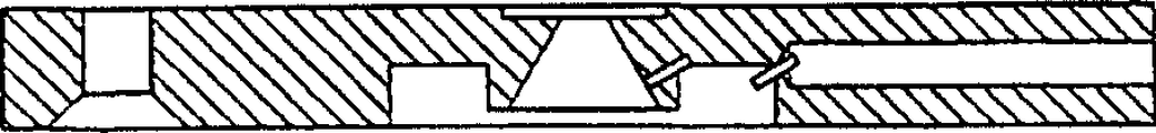
Referring now to Fig. 1,, Fig. 1 is the general schematic view of longitudinal section of the sample area of expression prior art SEM 10.Once electron beam 12 is advanced by the vacuum path and is arrived sample 14.This electron beam bump sample 14 is to form a succession of back scattered electron 16, its bump back scattered electron detector 18.Except back scattered electron, the secondary electron of being launched by sample 20 quickens to secondary electron detector 22.
The mean free path of the electronics by atmosphere is very little, therefore be in the vacuum through the whole electron path of sample to detector from reflector, this just can not the wet sample of research or body in handle.
Referring now to Fig. 2,, Fig. 2 is the general schematic view of expression longitudinal section of the scanning electron microscopy of first scheme according to the present invention.Represent with identical reference marker with parts identical in the earlier figures, the mandatory declaration, no longer describe except being used to understand present embodiment.
In Fig. 2, once electron beam 12 is advanced by the sample 32 of vacuum chamber 30 in being placed on chamber 34.Being sealed in the chamber 34 is be fit to keep wet and atmosphere active mass, wherein can carry out handling in the atmosphere body.Only environment will comprise aqueous medium.
Separate in order to seal this chamber and vacuum chamber, the block piece 36 that is generally barrier film passes the hole that is limited by ring 38 and extends.Ring 38 is designed in its end to keep barrier film 36 with air tight manner, as shown in more detailed below in conjunction with Fig. 3.Sample 32 is preferred near barrier film 36 placements, makes electron beam needn't pass the atmosphere in the chamber, so that reach sample.In a preferred embodiment, sample 32 contacts with the barrier film actual physics, and under the situation of active mass, can adopt known method to be grown on the barrier film or is fixed to the upper, and is as described below.
Preferably, chamber 34 comprises exhaust outlet 40, describes this parts in detail below in conjunction with Fig. 3.It also comprises inlet 41 and the outlet 42 that is used for fluid, and fluid is kept for the appropraite condition of sample.For example, can utilize inlet 41 and outlet 42 to change the chemical environment that is studied sample.This feature is particularly useful on the medicine in research, there, along with the change of given drug concentration can observation of cell dynamic response.
Secondary electron (SE) generally has than the low energy of aforementioned those electronics, and often is absorbed in the water usually.Therefore detect less than SE usually from the sample emission.Yet in a preferred embodiment, one or more layers has the material 37 of high secondary electron productive rate by coating on barrier film, strengthens the SE signal.Typical material comprises lithium fluoride.
Obviously, SE is detected by SE detector 22, and therefore is used to strengthen whole signal.
In a preferred embodiment, the diameter that exposes the zone of the barrier film in the hole 36 is essentially 1-3mm.Barrier film is supported on the screen usually, and each opening in the screen has the maximum gauge that is about 0.1mm.Screen has strengthened the ability that barrier film bears barometric gradient.Screen schematically is shown among Fig. 3.
Barrier film preferably allows to keep the ordinary atmospheric conditions of chamber 34, and therefore allows to detect to comprise competent cell, organelle or its parts and protein.It also allows to detect surfactant, colloid, oil particles, latex and polymer or micellar solution.In pharmaceutical industries, this chamber for example can be used to check the dynamic property of medicine, and as swelling, dissolving and decomposition, even cell is to the resistance of some drugs.In textile industry, this chamber can be used for studying hair, cotton and synthetic fibers wet and that do.The present invention other field applicatory can comprise oil, food, geology, microelectronics, paper coating and material science.
Available desirable gas of chamber 34 itself or liquid filling, and because the nanometer range resolution of electron beam and can monitor sample at molecular level.Can ignore by the resolution loss that barrier film causes, because scattering events wherein takes place hardly.When filling this chamber with gas, preferably the decompression device that comprises spring 43 and additional barrier film 44 can be set in chamber, break so that prevent barrier film 36.
According to embodiments of the invention, chamber 34 can be attached among the standard SEM, as following with reference to as described in Fig. 3.Chamber 34 compatibility standard sample holders or sample installing rack.Sample holder is according to the size design of normal business sample holder, so it can be easy to be attached to sample chamber, promptly is used for placing the microscopical shell of sample holder.
Though this chamber of front has been described to contain atmospheric pressure, whether all be necessary for all samples, in some cases, find that lower pressure also is fit to, therefore reduced the barometric gradient of passing barrier film 36.
Adopt electron beam to observe the difficulty of handling in competent cell or the body and be that electron beam itself will damage sample.For example, the maximum damage to DNA occurs in 4keV.Select the polyimide diaphragm of 3keV/1500 dust to be in safely below the maximum level of damage.
Make the minimized energy level of the damage of independent sample by discovery, level of damage can be further optimised.
Referring now to Fig. 3, Fig. 3 is the simplification of another embodiment of chamber of Fig. 2 and the more detailed sectional view that amplifies a little.The gravel size decision of chamber 50 can be assembled in the conventional sample fixer, and this chamber 50 comprises sample fixation kit 51, and this assembly 51 comprises the body member 52 that seals sample area 54, and sample area has open surfaces 55.In the example of Fig. 3, body member 52 is SEM sample installing racks of standard.Sample area is by barrier film 56 sealings of aforementioned type, and it is assemblied on the exposed side of sample area 54.Screen 59 is positioned on the barrier film and by dividing plate 57 and separates.Closure member 58 is assemblied on the body member 52 in the mode around its edge chucking barrier film 56.Screw 62 in the respective aperture of closure member in being assembled to closure member 58 is fixed on the body, and wherein hole in the closure member 58 and the screwed hole 60 in the body member 52 are continuous.For the gas-tight seal in sampling district 54, O shape ring sealing gasket 66 is assembled in the body member 52 around sample area 54.
The sample 64 that illustrates is closely close with barrier film 56.Preferably, it should be in fact to contact with barrier film or be in the nanometer range, so that electron beam needn't be advanced by the air of any a great deal of.
When during the sealed sample district, may in sample area, producing pressure by tightening screw 62.Therefore provide pressure relief assembly 68, so that discharge excess fluid.Assembly 68 comprises the sleeve 70 of closed channel 72.Passage 72 is connected sample area 54 with another opening 74 at the far-end of sleeve 70.Around sleeve 70 is sliding cylinder closure member 76, and this closure member 76 comprises and being assembled on the lower member 79 so that relative the 2nd O shape ring sealing gasket 78 inwardly compresses its upper-part 77.76 preferred of closure members are used for sealed open 74 after sample area itself is sealed, allow the path that is used for excess fluid of sample fixation kit 51 thus.
Connector 73 is convenient to be inserted in the sample fixer (not shown).
Referring now to Fig. 4, Fig. 4 is the embodiment of the chamber of Fig. 2 and 3, is applicable to the additional sample of being undertaken by Optical devices.In Fig. 4, chamber 80 is as the part of photoconduction 82 and make.86 fixing barrier film 84 sealed chamber 80 keep vacuum by closure member.One end of reflectance coating 90 preferred coated photoconductions 82, the other end leads to the photomultiplier (not shown) along the direction of arrow 92.Sample 94 usefulness electroluminescence (fluorescence) marks are done mark, and this mark is by electron-beam excitation.Light along the direction deflection of arrow 92 to be amplified by the photomultiplier (not shown).Therefore can detect single photon, and preferably be provided for carrying out the device of optical detection with the nanoscale resolution of SEM.
Referring now to Fig. 5,, Fig. 5 is that the wet electron micrograph of pattern detection of embodiment shown in Fig. 3 is adopted in expression.Sample is an oil emulsion in the water, as is used in previous experiments to show the sample of ESEM comparative, by Matthews (Proceeding of Institute of Physics, EMAG99, the 95th page, Sheffield, 1999) described, it is for reference to quote its full content here as proof.This electron micrograph is to take with JEOL 8400 SEM with low resolution, and shows scale designation.Employing is in fact identical with the level of resolution that adopts SEM to realize in not having the usual manner of barrier film according to the resolution that barrier film of the present invention obtains.Obtain good comparative, and the long and is enough for wet pattern detection.
Should be appreciated that, for clarity sake, each feature of the present invention described in each embodiment can also with the combined setting of single embodiment.On the contrary, for simplicity, also can independently be provided with or be arranged in any suitable sub-portfolio in each feature of the present invention described in the single embodiment.
The detailed description of the preferred method of the present invention
Ideally, be used for should providing following performance to the technology of the wet sample imaging of the on-fixed cell that includes, but is not limited to live:
1, imaging performance:
At least the resolution of 100nm is preferably in the 1-20 nanometer range
High s/n ratio and signal and background ratio
2, cells physiological environment:
The ability of in the wet environment of wet on-fixed cell, working
Minimized radiation damage (to the least interference of imaging, to result's biological related minimum influence)
3, output
The minimal sample preparation process.
The automation strategy
The present invention is based on scanning electron microscopy, we have revised it makes it satisfy above-mentioned standard.
The minimal sample preparation process
Traditional SM program needs sample application charged to prevent it.Here, the water electrolysis liquid (medium) of encirclement cell is enough to prevent charged.Like this, sample preparation does not need applying step, and allows to work with competent cell.Compare with conventional SEM, the fact that sample preparation does not need to fix, dewater or apply shortens significantly and has simplified the sample preparation program, and has improved result's quality greatly.Sample preparation program as unrestricted example is arranged here.This example is suitable for making marks to the extracellular cell component, as the extracellular part of barrier film protein.Other labelling technique comprises to the cell within a cell composition and making marks in following example introduction is arranged.Pair cell makes marks and is undertaken by the immune labeled program of rule.
Our result shows that this wet SEM technology is suitable for fixing and competent cell, and is suitable for adhering to and non-adherent cell.In addition, although these results show that mark must have individual molecule and detect, pair cell imaging under the situation of mark can not had.
The automation strategy
The present invention has also solved the low-yield problems of experiment SEM.The SEM automation that the present invention is utilized as the semi-conductor industry development of wafer inspection is used for biological sample.This idea that is utilized as the SEM automation of wafer inspection development in biology applies for being illustrated in detail in (PCT/IL01/00764) at the PCT that examines jointly that themes as " method and the equipment thereof of identification and quantification biomolecule ".Wherein, sample is done, for use in " wafer inspection scanning electron microscopy " (WISEM) or the microscopical clear and definite purposes of WISEM class.This idea can not be applicable to the biological sample that obtains in their natural water-bearing environment, because the preparation of this sample should meet the vacuum requirement of conventional electrical microtechnic, comprise WISEM, applies fierce and complicated step and may hinder automation.The present invention can carry out imaging to aqueous specimen, and does not need these doubt sample preparation steps.Like this, permission is utilized as the SEM automation of the semi-conductor industry development of wafer inspection in biology.This use will greatly reduce the cost of the required equipment of this method of realization.
Automation strategy (automation strategy) is to be described in to utilize WET SEM technology to carry out one group of guide of the program used in the automated imaging of competent cell sample.In a preferred embodiment of the invention, automated procedures will comprise: contain " cell chip " of a large amount of isolated chamber, wherein each chamber contains the sample of promising wet SEM imaging preparation.The separation barrier film of auxocyte sample (can be identical or different) is thereon contained in each this branch (isolated chamber).
When the preparation sample, can adopt the control of standard automatic fluid.
In case cell chip prepares to be used for imaging, it just can adopt the normalized optical microscope or be integrated into special setting among the SEM (as optical fiber etc.) and carry out automated optical imaging (or low multiplication factor SEM scans).This scanning will provide the overview image of the cell in each chamber, their position and any out of Memory relevant with experiment.Information about cell in this scanning will adopt the algorithm of special development to detect automatically.
Separate barrier film and be installed on the metal grating, so that realize mechanical stability.Screen is the coordinate benchmark that facilitate, extremely stable of each image.
Carry out in the SEM outside under the situation of optical scanner, cell chip is sent in the SEM chamber, is used for the SEM imaging.Calibration algorithm will be used for mating between the coordinate system of light microscope and SEM.
In case these two coordinate systems have mated, SEM will carry out imaging to the interested appointed area of selecting automatically according to optical scanner (or low multiplication factor SEM scanning) (ROI).Special sub-positioned area during this ROI can comprise the intracellular appointed area that important biological activity takes place or relate in the cell or the zone that provides other the regional statistics in the cell to represent.Gold colloid will imaging in each this zone.
This ROI can be of different sizes, and therefore needs the SEM of different magnification ratios.Notice, can between the size of imaging viewing field and observable mark, trade off.Therefore, for carrying out the different size that imaging will need mark in different visual fields.Particularly, for the imaging of whole single cell, need big visual field.This big visual field means magnification ratio and only observes the ability of big gold colloid (resolution that depends on scanning).Perhaps, a lot of small field of view images of obtaining with higher magnification ratio can make up, so that the high resolution picture of whole cell to be provided.
The SEM image is automatically snapped.This comprises automatic location, automatic focus and astigmatic correction, auto brightness and the contrast of SEM operating desk.
Can adopt image analysis algorithm to analyze the image of taking by SEM automatically.This comprises the position of observed gold colloid and discriminating, calculating and the contrast of size.
In the SEM imaging, can also measure other signal.These signals comprise from the signal of cathodoluminescence mark (as described below) or from the X ray of sample to be launched, but the analytical chemistry analysis of this sampling.
When utilizing cell chip of SEM scanning, can scan another by optical mode.
Ultrahigh resolution optical imagery in SEM
Making us very interested selection is to adopt narrow beam excitation light emission in sample.This light emission is called as cathode emission, and (cathodoluminiscence CL), and has carried out studying (, scanning electron microscopy I, 257,1977 described by Hough PVD) to the dehydration sample in the past.This can be to detect the light emission than the better resolution of the one theory in the light microtechnic.This scheme combination the high-resolution of SEM imaging and common fluorescence labeling.When in SEM wet and active sample being carried out imaging, this selection scheme is highly beneficial.In this imaging system, electron beam produces secondary electron (SE) emission, excites CL (fluorescence) labelled molecule, and and then visible emitting.The light of this emission is collected in and uses the collection path that detection of electrons separates always then.Can show and broadband UV radiation equivalence (seeing Hough PVD, scanning electron microscopy I, 257,1977) by exciting of carrying out of secondary electron.The advantage of this method is as follows:
1, the combination of fluorescence and golden mark has a lot of biological advantages.
2, the high-definition picture that obtains to be labeled molecule can provide new and important biological information.
3, single-photon detects the quite most recovery of the photon of being managed easily and guaranteeing to launch.
4, the availability of dna encoding fluorescence protein has represented the new marker meeting of electron microscope technique.
5, application specific probe such as quantum dot and fluorescent bead can be used as mark in this technology, are provided at unavailable multifunctionality and advantage in other technology.
The embodiment of wet-CL device can maybe can comprise the development of new collection geometry and structure based on existing CL detector.Existing detector for example is those detectors of collecting light from poincare half plane (above the sample).In this minute surface configuration, ellipsoidal mirror is placed on the sample top, wherein has aperture to pass through to allow electron beam.Light collected by this mirror and the microscope that leads in window, at the outer setting photon detector of window.This collection structure can obtain from the market, for example from Gatan company (previous Oxford instrument company).Below we discuss and to be used for two schematic construction that demifacet is down collected, wherein photon is collected below sample, and by the detector of optical guide guides light to the microscope outside.
The manufacturing of this device is as follows: sample chamber (being made of stainless steel) by separating diaphragm seals, is sealed by lenslet on lower member, so that barrier film is arranged in the focussing plane of lens on upper member.Like this, emission and the light collected by lens penetrate near barrier film, and are calibrated when leaving lens.Sample chamber is placed on operating desk inside, and wherein the prism light that will penetrate lens guides once more with an angle of 90 degrees degree (being level).
Operating desk also contains lens, is used for focusing on the light of optical fiber porch again.Optical fiber leads to the detector that is positioned at the microscope outside from operating desk.The detector that uses is a single photon module detection system.For each detected photon, output signal is TTL signal (a 0-5V square-wave signal).
The output of detector is connected to computer socket, and computer socket calculates the quantity of the TTL signal (photon) that receives.Computer socket also receives from microscopical several signals: the beginning of image acquisition; The beginning of new frame; The beginning of newline.Adopt the suitable software of particular design, according to collecting the data in real time reconstructed image.
Fig. 6 represents to have the sample chamber of assembling different parts a-E together.Single parts have detailed introduction in Fig. 7 A-E.
Assembling is used for the structure of fluorescence experiments
Fig. 7 (S-E) expression is used for first embodiment of the assembly of fluorescence experiments.
It is several millimeters hole that components A contains diameter in a side, and it is placed upside down on desk.Part B is placed on inner screw with careful aligning parts A and B.Two O shape rings are inserted in the part B.Barrier film is suitably placed.Barrier film is installed on the plastic stent that thickness is 0.1mm.The diameter of plastic stent must be selected between two diameters of the O shape ring that uses.Forming diameter in advance in the middle of plastic stent is the hole of 3mm, and this is the zone that does not have barrier film.The TEM screen is bonded on barrier film one side (outer side) in the middle.Insertion parts C then.It is very important that horizontal duct is aimed at the side opening of components A.Insert 6 screws.Barrier film, components A, B are screwed with C and are in the same place.Prepare water or any other aqueous medium filling sample then.Liquid medium is in the free space inside deposition (it still is inverted) of the centre of parts C.Insert fine needle (diameter is 0.1mm) by the hole that on the side of components A and C, forms.Pin inserts inner darker position, up to its wet chamber of end arrival.Another end of pin is positioned at the outside.Last O shape is encircled on the tram that is placed among the parts C.(in this stage, O shape ring can not be in place fully, because pin there, just in time is positioned at it down.This is very normal, and useful for the following step).Parts D (comprising that at the middle part lens are not shown with alignment light----) is placed in the assembly.Got wet by the medium of filled chamber in the inboard of lens.Last insertion parts E.When turning part E in assembly, parts D (having lens) is pressed on (parts C's) O shape ring gradually.Owing to O shape ring does not have in placely fully because of pin, so it also can not make chamber and external discrete.When tightening parts E, the volume of wet chamber reduces, and therefore excessive medium can flow out below the O shape ring of pin.Usually, the conduit from parts C flows out some drop.When fully compressing O shape ring and lens and correctly locate, pin is slowly pulled out.In this stage of assembly, the O shape ring in the part B can freely occupy institute and have living space.It enters its normal position, its sealed chamber in this position.Like this, at last in complete sealed chamber of this stage.(components A-E) forwards its normal position (upper end up) to and is inserted as in its specially designed microscope work platform with this assembly then.
Fig. 8 represents to be suitable for the microscope work platform that uses with assembly.The chamber, top of operating desk (2) is the groove that wherein inserts sample chamber.In its lower section be prism.Prism (1) is used to make light to change direction along the direction in hole.In this hole, the lens (not shown) makes light focus in the porch of optical fiber.
In order to obtain higher light collection efficiency, designed a kind of interchangeable structure, wherein between biological sample and photoconduction, set up directly coupling.This interchangeable structure is shown among Fig. 9.It comprises the vacuum tight chamber, and light is from the above-mentioned single-photon detector arrangement of the direct directive of sample area.In the figure, adopt screw (6,7) that shell (1) is fixed on support (2) and the lid (3), inside is provided with chamber dish (4), and has barrier film, further is connected to photoconduction (5), with O shape ring (8) sealing.
Labelling technique
The present invention is suitable in the cell of cell or pair cell composition imaging in the part of extracellular.
Can consider that different schemes makes marks to the intracellular portion of cell:
If cell can use in fixing back, then common method comprises the infiltration or the extraction of cell film.
The another program that is suitable for competent cell is to insert mark by pinocytosis (pinocytoic) reaction.Then can be when it be active fixed cell or observation of cell.If carry out under suitable condition, the pinocytosis reaction has kept the viablity of cell.It allows to insert molecule (great majority known in the art are fluorescence labeling in using) or nanoscale particle (as being particularly suitable for the application).Some researchers have reported the globule of successfully introducing micro-meter scale in cell.
Infiltration and extraction procedure are suitable for fixed cell.Can adopt several programs, this depends on whether the operator thinks to remove fully the cell film or only produce some holes.
Extract and fixedly mean the outside film of removing cell at first fully.Then, fixed cell at once.This program helps presenting the structure in cytoplasm, nucleus or the cytoskeleton.
Fixing and infiltration means at first fixed cell, and it is permeable then the cell film to be become.
The pinocytosis reaction is suitable for competent cell.For example, can adopt reagent (as commercially available Influx (injectant)) (molecular probe 1-14402) so that particle is introduced in the cell.Inject of the infiltration dissolving of cell bearing technology based on pinocytotic vacuole.In brief, the compound that load oozes medium with high concentration and height to be mixed, and allows by pinocytotic vacuole (vesicle) this material to be imported in the cell.These cells are sent to hypotonic medium then, and this causes discharging the material of catching from intracellular pinocytotic vacuole, with compound tytosis solute.
Abide by the agreement that " molecular probe " provides, we are incorporated into the gold grain of " collaurum ", hundreds of nano-scale, the fluorescence globule and the quantum dot of micron-scale in the cell.Cell can be fixed and strengthen golden or silver-colored before observing.When adopting this method, a certain proportion of cell death.In the most experiments of carrying out, loss is no more than the cell of 10-20%.
The gold grain that available pair cell has a low damage makes marks to the cell surface of competent cell.Have a kind ofly for be used in combination the signal agreement of developing with the present invention, it utilizes the streptavidin labeling method, as is known in the art.This idea is to cultivate cell with biotin, and biotin will adhere on the protein of the certain percentage on the cell surface.Then, cultivate cell with the streptavidin that is linked to gold grain, wherein gold grain will adhere on the biotin.Must carefully control the dosage of the biotin that is used to cultivate, because the too many biotin on the film protein may be upset the active of them and cause cell death.Different research has shown that biotin can be used for tracking cell and uses.Several research relates to red blood cell (people such as Hoffmann-Fazer for example, hematology annual report, 74,231-238,1997; Ault, K.A. and Knowles, the Exp hematology, 23,996-1001,1995, for reference here).Biotin makes marks for a lot of cells and their biological property is had seldom or not change, and allows when needed to detect them and recover them.
Micro-column.With another research that productivity ratio is increased be and the parallel detection that utilizes micro-column.Micro-column is the miniscanning electron microscope of being made by integrated silicon technology.Because their size, micro-column can parallel work-flow; Sweep time and bulkiness have been significantly reduced based on the system of SEM.The further describing of micro-column " microelectronics optics " at Feinerman and Crewe, the progress of imaging and electron physics, the 102nd the volume, 187 (1998) and U.S. Pat 5122663 in introduction is arranged, the full content of quoting these documents here as proof is for reference.Thisly in biologic applications, utilize idea based on the electron microscope of micro-column to be called examining in the PCT application (PCT/IL01/00764) jointly of " identification and quantize the method and the device thereof of biomolecule " in name introduction is arranged.
The example of principle of the present invention below is provided, only be used for illustrative purpose and nonrestrictive.
Example
Auxocyte on barrier film
Be the schematic procedure of auxocyte on barrier film that provides as unrestricted example below.At first use fibronectin (0.1mg/ml) coating polyimide to separate barrier film 15 minutes.After PBS and culture medium cleaning, use common method, with the concentration coating cell of 800-1500 cell in every chamber 12-15 μ l.After 24 hours, cell beamhouse operation/make marks.Most cell types can separated originally growth on one's body and without the support of additional matrix (as fibronectin) of barrier film, still under this condition, and their easier being cleaned during the cleaning procedure on a large scale.The viablity of cell is not subjected to the influence of these any operations.
Compatibility of the present invention depends on or the non-cell (as described below) that depends on.For realizing the non-purpose that depends on cell (for example lymphocyte) imaging, at first in suspension, make marks to cell, in 30 minutes, allow to bond to then and separate on the barrier film, this barrier film was with 0.4% polylysine preliminary treatment 1-3 hour.
Minimize radiation damage
We have for example understood the only imaging power of the undisturbed processing on short time yardstick (second) at present.A kind of radiation damage that must consider is the damage by free-radical generating, and this free radical is formed by electron beam bump hydrone.
One that prevents this damage may strategy be to make to comprise the additive that can absorb the free radical that is produced by radiation in the cell medium, and the radiation damage of pair cell is minimized.Any known compound that is suitable for removing group all can use, as long as its pair cell is nontoxic.An example that is used for this additive is a sucrose, and it has been counted as the free radical absorbent.This scheme is only to be used for the present invention, because conventional electrical bundle technology can not be worked under wet environment.
Make marks to cell by immune labeled
Make marks to cell and to be undertaken by the immune labeled program of rule.Clean cell, and randomly fix 7 minutes by 2% paraformaldehyde.After suitable serum sealing, cultivated cell one hour with special list or polyclonal antibody.After the cleaning, cultivate sample with the second antibody that is different from first distinct antibodies.This second antibody is linked to one 5,10,20 or 40nm gold group on.Be adopted as the condition of the careful calibration of every kind of colloid then, can further amplify golden mark by silver-colored reinforcing agent.
Separating wet cell fixing under the barrier film
The growth factor receptor is marked on fixing A431 cell and the C2C12 mouse sarcoblast.
Paraformaldehyde fixed cell with 2%, and make marks with anti-FGF acceptor monoclonal antibody (on the C2C12 sarcoblast) or anti-EGF monoclonal antibody (A431 cell), be connected on the gold colloid of 20nm diameter by anti-mouse IgG then.Cell is fixed, and adopts silver-colored reinforcing agent to increase the size of marking particle.XL30 ESEM is used for imaging, and with back scattered electron (BSE) pattern examination cell.FGF receptor gold mark can be used as bright spot and sees on the cell shown in Figure 10 A.The EGF receptor is visible on the A431 of Figure 10 B-D cell.Mark around the nuclear area is smudgy to be that structural difference between the gold grain causes.Near the golden mark of barrier film is clearly and clearly, and around the nucleus and the mark of more far-end in addition be ambiguous.Mark in nuclear area is smudgy to have proved that mark in this zone is away from separating barrier film.In fact this is smudgy provides the instrument of the distance on the plane that is used for definite marking path barrier film, thereby three-dimensional information is provided.Employing can make and add the image analysis algorithm that the effect of medium between barrier film and mark deconvoluted, and the accurate assessment of this distance can be provided.
For being implemented in the more high-resolution image of the mark on the cell distally (relative), can adopt other chamber design with a side that is fixed to the barrier film bottom.In this design, cell is grown on the platform that has only the thin layer liquid that covers them.Then, the separation barrier film is placed on the top of the platform that covers cell.In this way, make the top side imaging of cell, and cell is in the wet environment still.
The adherent cell that activity under barrier film does not make marks
Active C2C12 mouse sarcoblastCell is applied on the fibronectin in their normal culture mediums.After 24 hours, with BSE mode detection cell.Clear outline line and its nucleus and the organelle of some daughter nuclei that shows cell of active C2C12 cell (Figure 11 A-D) and Chinese hamster ovary celI (Figure 12).
The IL-2 acceptor α of mark on Jurkat (T lymphocytic series) human lymphocyte
Mark to cell with anti-human body IL-2 acceptor monoclonal antibody, will resist mouse IgG to be connected to diameter then is on the 20nm gold colloid.Allow cell contact to polylysine precoating barrier film last 30 minute, use the BSE mode detection then.Figure 13 represents the golden mark of the focusing that passes in and out, and it is obtained by the structural difference between the EGF receptor marker (Figure 10 B-D) of gold grain of seeing in the FGF of aforementioned fixation C2C12 receptor marker (Figure 10 A) and A431 cell.
The image that obtains with this cathodoluminescence (CL) structure.
Even signal very weak (possibility is owing to low light collection efficiency causes), but clear view cell.Also can observation of cell (some part that is cell is luminous automatically) even without the CL mark.Utilize CL mark and improved collection efficiency, can obtain higher resolution.
The cathodoluminescence image of fixed cell NIH3T3.There is not luminescent marking to insert cell.Therefore, only the obtaining from " nature " cathodoluminescence of cell of emission is shown in Figure 14 A-C.The cell width is about 20 microns.
Based on biotin mark on the NIH3T3 cell:
Material:
Sulfo--NHS-LC-biotin (B1022 of Sigma) (in DMSO, dissolve 10mg/ml and remain on 4 C).
Streptavidin, the link diameter is the gold grain of 10nm-40nm.
Phosphate buffer normal saline (PBS), preheating under 37 C.
The culture medium (under the cultivation temperature, being the clone preheating) that is used for clone.
The serum free medium of preheating.
Preparation solution:
Solution A: sulfo--NHS-LC-biotin is with the PBS of 0.5mg/ml in preheating.Solution must prepare before using, because can degenerate in water.
Solution B: streptavidin gold (1/10 to 1/100) is dissolved in the PBS+ serum free medium (1-5 volume ratio).
Solution C: full culture medium-PBS solution (1-5 volume ratio).
Program:
1, the trypsinization of cell.
2, carried out centrifugal action 4 minutes with 1250t/ minute.
3, remove supernatant liquor and suspension again in the 10ml fresh culture.
4, getting 3m1 divides into two 1.5ml microcentrifugal tubes.
5, carry out reaching 3 minutes in centrifugal action 1600t/ minute.
6, remove supernatant liquor as much as possible.
7, add PBS lightly in pipe, to obtain 1.5ml (cleaning) at 37 degree.Suspension cell again.
8, carried out centrifugal action once more 3 minutes.
9, remove PBS and adding biotin (solution A).Suspension cell and mixing lightly and well again.
10, under 37 degree, cultivate 20 minutes (shaking once in per 3 minutes).
11, carry out centrifugal action
12, remove supernatant liquor and suspension again in the fresh culture of 1.5ml
13, being sent to Petri dish or barrier film also cultivated several hours at night.
14, clean 1 to 2 time with PBS.
15, cultivated 1 hour with solution B, if possible can mix sometimes.
16, clean 1-2 time with PBS.
17, remove PBS and replace with solution C.
18, under electron microscope, begin to observe.
Active NIHT3 cellThe pair cell surface protein carries out biotinylation, and is linked to streptavidin, and it is fixed on the gold grain of 40nm, as shown in figure 15.
Those of ordinary skills know, the invention is not restricted to the example that the front illustrates especially and introduces.Scope of the present invention comprises aforementioned each combination of features and sub-portfolio and various change of the present invention and modification, and these changes and modification are attainable after having read above stated specification by those skilled in the art, and not record in the prior art.
Claims (40)
1, a kind of chamber of using with scanning electron microscopy of being suitable for, described chamber comprises at least one hole, this hole diaphragm seal, described barrier film is suitable for bearing vacuum, and is electron permeable, the inside of wherein said chamber and described vacuum insulation.
2,, be suitable under atmospheric pressure, holding water basically according to the chamber of claim 1.
3,, wherein has diameter in the 0.1-4mm scope with the described hole of described diaphragm seal according to the chamber of claim 1.
4, according to the chamber of claim 1, wherein said barrier film has the thickness in 200-5000 dust scope basically.
5, according to the chamber of claim 1, wherein said barrier film comprises the material that is selected from polyimides, polyamide, polyamide-imides, polyethylene, polypyrrole and additional conductive polymer, parlodion, collodion, Kapton, FomrVar, Vinylec, ButVar, Pioloform, polyvinyl acetal, silicon dioxide, silicon monoxide and carbon.
6, according to the chamber of claim 5, its septation is a polyimides.
7,, be included near the sample of laying the barrier film according to the chamber of claim 1.
8,, comprise with described barrier film contacting the sample of laying according to the chamber of claim 1.
9, according to the chamber of claim 1, wherein said barrier film is by the support grid support that is placed between barrier film and the vacuum.
10,, can be placed in the vacuum and the sample in fluid-encapsulated according to the chamber of claim 1.
11,, can be placed in the vacuum and sealing sample under the atmospheric pressure basically according to the chamber of claim 1.
12, a kind of chamber that is used in combination with scanning electron microscopy, at least a portion of the wall of wherein said chamber can be resisted an atmospheric pressure gradient, and has the electron permeable of the energy that is higher than 2keV.
13, a kind of device that adopts scanning beam to use in chamber middle high-resolution ground inspected object comprises the vacuum path of electron beam and combines the vacuum-resistant block piece of placing with object that described vacuum-resistant block piece is set up so that object and vacuum insulation.
14, according to the device of claim 13, wherein object comprises one of fluorescence and electroluminescence mark, makes electron beam energy excitation light emission thus.
15, according to the device of claim 13, also comprise optical pickocff.
16, according to the device of claim 13, wherein said chamber comprises the part of photoconduction.
17, according to the device of claim 15, wherein said optical pickocff comprises photomultiplier.
18, according to the device of claim 15, wherein said optical pickocff is suitable for the single photon of sensing, and described device be suitable for thus sensing by the excitation of individual molecule produce luminous.
19, according to the device of claim 13, wherein apply block piece with at least one layer material with Senior Two time electronics productive rate.
20, according to the device of claim 13, wherein block piece is suitable for bearing the barometric gradient a barometric pressure range.
21, according to the device of claim 13, wherein said block piece is a barrier film.
22, according to the device of claim 21, wherein said film comprises the material that is selected from polyimides, polyamide, polyamide-imides, polyethylene, polypyrrole and additional conductive polymer, parlodion, collodion, Kapton, FomrVar, Vinylec, polyvinyl butyral resin, Pioloform, polyvinyl acetal, silicon dioxide, silicon monoxide and carbon.
23, according to the device of claim 22, its septation is a polyimides.
24, according to the device of claim 21, wherein said barrier film is reinforced with the reinforcing screen that is placed between described barrier film and the described vacuum.
25, according to the device of claim 21, wherein said barrier film has the thickness in the 200-5000 dust scope.
26, according to the device of claim 25, wherein said thickness is in 500-1500 dust scope.
27, according to the device of claim 13, wherein said block piece crosses the diameter hole in the 0.1-4mm scope and placing basically.
28, according to the device of claim 27, wherein said diameter is essentially 1mm.
29, according to the device of claim 13, wherein said block piece is that high energy electron is transparent.
30, according to the device of claim 13, wherein said block piece is what to be had above the electron permeable of the energy of 2keV.
31, according to the device of claim 13, wherein said block piece is what to be had above the electron permeable of the energy of 3keV.
32, according to the device of claim 13, wherein said block piece applies with the layer of material with Senior Two time electronics productive rate.
33, according to the device of claim 32, the described material that wherein has high secondary electron productive rate is a lithium fluoride.
34, according to the device of claim 13, wherein the scavenger molecule is set up with described block piece and combines.
35, according to the device of claim 13, wherein object contacts placement with described vacuum-resistant block piece.
36, a kind of method of observing wet object with nanometer range resolution, may further comprise the steps: separate described chamber and vacuum chamber by adopting block piece, wet object is isolated in the chamber, provide electron beam so that clash into described sample from described vacuum chamber, and observe at least a of the secondary electron that penetrates from described chamber and back scattered electron by described block piece.
37, according to the method for claim 36, wherein said block piece comprises barrier film, and it is selected bearing a basic atmospheric pressure, and is what to have above the electron permeable of the energy of 2keV.
38, according to the method for claim 36, wherein wet object comprises drug ingedient.
39, according to the method for claim 38, wherein wet object also comprises drug ingedient reactive activity cell with it.
40, according to the method for claim 38, wherein said chamber comprises fluid intake, and drug ingedient at viewing duration with respect to dynamically one of the concentration by this inlet and type are changed.
Applications Claiming Priority (4)
| Application Number | Priority Date | Filing Date | Title |
|---|---|---|---|
| US25087900P | 2000-12-01 | 2000-12-01 | |
| US60/250,879 | 2000-12-01 | ||
| US30645801P | 2001-07-20 | 2001-07-20 | |
| US60/306,458 | 2001-07-20 |
Publications (1)
| Publication Number | Publication Date |
|---|---|
| CN1511332A true CN1511332A (en) | 2004-07-07 |
Family
ID=26941209
Family Applications (1)
| Application Number | Title | Priority Date | Filing Date |
|---|---|---|---|
| CNA018199062A Pending CN1511332A (en) | 2000-12-01 | 2001-11-30 | Device and method ofr examination of samples in non-vacuum environment using scanning electron microscope |
Country Status (10)
| Country | Link |
|---|---|
| US (3) | US6992300B2 (en) |
| EP (1) | EP1340241B1 (en) |
| JP (2) | JP4153303B2 (en) |
| CN (1) | CN1511332A (en) |
| AT (1) | ATE510298T1 (en) |
| AU (2) | AU2002221019B2 (en) |
| CA (1) | CA2436237A1 (en) |
| CZ (1) | CZ20031455A3 (en) |
| IL (1) | IL156027A0 (en) |
| WO (1) | WO2002045125A1 (en) |
Cited By (5)
| Publication number | Priority date | Publication date | Assignee | Title |
|---|---|---|---|---|
| CN101545874B (en) * | 2008-03-28 | 2013-09-25 | Fei公司 | Environmental cell for a particle-optical apparatus |
| CN104076049A (en) * | 2013-03-26 | 2014-10-01 | 三星显示有限公司 | Inspection system using scanning electron microscope |
| CN105810542A (en) * | 2014-12-10 | 2016-07-27 | 财团法人工业技术研究院 | Electron microscope with stage |
| TWI594288B (en) * | 2016-03-14 | 2017-08-01 | 台灣電鏡儀器股份有限公司 | Electron microscope |
| CN109187595A (en) * | 2018-09-27 | 2019-01-11 | 南京宁智高新材料研究院有限公司 | The device of local equivalents pressure caused by micro- gas beam in a kind of measurement transmission electron microscope |
Families Citing this family (136)
| Publication number | Priority date | Publication date | Assignee | Title |
|---|---|---|---|---|
| GB2367686B (en) * | 2000-08-10 | 2002-12-11 | Leo Electron Microscopy Ltd | Improvements in or relating to particle detectors |
| IL150056A0 (en) | 2002-06-05 | 2002-12-01 | Yeda Res & Dev | Low-pressure chamber for scanning electron microscopy in a wet environment |
| WO2003104848A2 (en) | 2002-06-05 | 2003-12-18 | Quantomix Ltd. | Methods for sem inspection of fluid containing samples |
| US11243494B2 (en) | 2002-07-31 | 2022-02-08 | Abs Global, Inc. | Multiple laminar flow-based particle and cellular separation with laser steering |
| US20070125947A1 (en) * | 2003-02-20 | 2007-06-07 | David Sprinzak | Sample enclosure for a scanning electron microscope and methods of use thereof |
| US20050017173A1 (en) * | 2003-07-15 | 2005-01-27 | Nalin Kumar | Individually addressable nanoelectrode array |
| US7274447B2 (en) * | 2004-06-21 | 2007-09-25 | Swce | Material porosity pressure impulse testing system |
| US20060144778A1 (en) * | 2004-07-29 | 2006-07-06 | Grunthaner Frank J | Low stress, ultra-thin, uniform membrane, methods of fabricating same and incorporation into detection devices |
| US7626179B2 (en) | 2005-09-30 | 2009-12-01 | Virgin Island Microsystems, Inc. | Electron beam induced resonance |
| US7791290B2 (en) | 2005-09-30 | 2010-09-07 | Virgin Islands Microsystems, Inc. | Ultra-small resonating charged particle beam modulator |
| US7586097B2 (en) | 2006-01-05 | 2009-09-08 | Virgin Islands Microsystems, Inc. | Switching micro-resonant structures using at least one director |
| WO2006021961A2 (en) * | 2004-08-26 | 2006-03-02 | Quantomix Ltd. | Sample enclosure for inspection and methods of use thereof |
| NL1027025C2 (en) * | 2004-09-13 | 2006-03-14 | Univ Delft Tech | Microreactor for a transmission electron microscope and heating element and method for manufacturing thereof. |
| US7381970B2 (en) * | 2005-01-31 | 2008-06-03 | Summer Schneider | Specimen stage for charged-particle scanning microscopy |
| US20060172315A1 (en) * | 2005-02-01 | 2006-08-03 | Anderson Amy L | Methods for staining cells for identification and sorting |
| CN100511568C (en) * | 2005-05-09 | 2009-07-08 | 东捷科技股份有限公司 | Method and apparatus for operating and observing high voltage cavity in vacuum or low voltage environment |
| TWI277734B (en) * | 2005-10-26 | 2007-04-01 | Li Bing Huan | Method for observing living bodies using an electron microscopy |
| JP2007163447A (en) * | 2005-12-09 | 2007-06-28 | Lee Bing Huan | Ultra-thin liquid control plate for electron microscope |
| TWI275118B (en) * | 2005-12-09 | 2007-03-01 | Li Bing Huan | Sample box of electron microscope for observing a general sample/live cell |
| JP5425475B2 (en) * | 2006-02-02 | 2014-02-26 | シーイービーティー・カンパニー・リミティッド | Vacuum column maintenance device for electronic column |
| US7443358B2 (en) | 2006-02-28 | 2008-10-28 | Virgin Island Microsystems, Inc. | Integrated filter in antenna-based detector |
| US7876793B2 (en) | 2006-04-26 | 2011-01-25 | Virgin Islands Microsystems, Inc. | Micro free electron laser (FEL) |
| US7646991B2 (en) | 2006-04-26 | 2010-01-12 | Virgin Island Microsystems, Inc. | Selectable frequency EMR emitter |
| JP2007294365A (en) * | 2006-04-27 | 2007-11-08 | Jeol Ltd | Test piece inspection method, test piece support body, and test piece inspection device as well as test piece inspection system |
| JP2007292702A (en) * | 2006-04-27 | 2007-11-08 | Jeol Ltd | Apparatus, method and system for inspecting samples |
| US7723698B2 (en) | 2006-05-05 | 2010-05-25 | Virgin Islands Microsystems, Inc. | Top metal layer shield for ultra-small resonant structures |
| US7436177B2 (en) * | 2006-05-05 | 2008-10-14 | Virgin Islands Microsystems, Inc. | SEM test apparatus |
| US8188431B2 (en) | 2006-05-05 | 2012-05-29 | Jonathan Gorrell | Integration of vacuum microelectronic device with integrated circuit |
| US7710040B2 (en) | 2006-05-05 | 2010-05-04 | Virgin Islands Microsystems, Inc. | Single layer construction for ultra small devices |
| US7746532B2 (en) | 2006-05-05 | 2010-06-29 | Virgin Island Microsystems, Inc. | Electro-optical switching system and method |
| US7732786B2 (en) | 2006-05-05 | 2010-06-08 | Virgin Islands Microsystems, Inc. | Coupling energy in a plasmon wave to an electron beam |
| US7359589B2 (en) | 2006-05-05 | 2008-04-15 | Virgin Islands Microsystems, Inc. | Coupling electromagnetic wave through microcircuit |
| US7986113B2 (en) | 2006-05-05 | 2011-07-26 | Virgin Islands Microsystems, Inc. | Selectable frequency light emitter |
| US7728397B2 (en) | 2006-05-05 | 2010-06-01 | Virgin Islands Microsystems, Inc. | Coupled nano-resonating energy emitting structures |
| US7718977B2 (en) | 2006-05-05 | 2010-05-18 | Virgin Island Microsystems, Inc. | Stray charged particle removal device |
| US7656094B2 (en) * | 2006-05-05 | 2010-02-02 | Virgin Islands Microsystems, Inc. | Electron accelerator for ultra-small resonant structures |
| US7728702B2 (en) | 2006-05-05 | 2010-06-01 | Virgin Islands Microsystems, Inc. | Shielding of integrated circuit package with high-permeability magnetic material |
| US7741934B2 (en) | 2006-05-05 | 2010-06-22 | Virgin Islands Microsystems, Inc. | Coupling a signal through a window |
| US7679067B2 (en) | 2006-05-26 | 2010-03-16 | Virgin Island Microsystems, Inc. | Receiver array using shared electron beam |
| US7655934B2 (en) | 2006-06-28 | 2010-02-02 | Virgin Island Microsystems, Inc. | Data on light bulb |
| JP5084188B2 (en) * | 2006-07-04 | 2012-11-28 | 日本電子株式会社 | Sample holder, sample inspection method, sample inspection apparatus, and sample inspection system |
| US7450794B2 (en) | 2006-09-19 | 2008-11-11 | Virgin Islands Microsystems, Inc. | Microcircuit using electromagnetic wave routing |
| JP4850654B2 (en) * | 2006-10-23 | 2012-01-11 | 株式会社日立ハイテクノロジーズ | Charged particle beam device and sample holding device for charged particle beam device |
| JP2010509709A (en) | 2006-10-24 | 2010-03-25 | ビー・ナノ・リミテッド | Interface, method for observing an object in a non-vacuum environment, and scanning electron microscope |
| JP5002251B2 (en) * | 2006-12-06 | 2012-08-15 | 日本電子株式会社 | Sample inspection method and sample inspection apparatus |
| TWI330380B (en) * | 2006-12-07 | 2010-09-11 | Nat Univ Tsing Hua | A specimen kit for electron microscope and its fabrication process |
| JP2008153086A (en) * | 2006-12-19 | 2008-07-03 | Jeol Ltd | Sample inspection device, sample inspection method, and sample inspection system |
| EP1936363A3 (en) | 2006-12-19 | 2010-12-08 | JEOL Ltd. | Sample inspection apparatus, sample inspection method, and sample inspection system |
| US7659513B2 (en) | 2006-12-20 | 2010-02-09 | Virgin Islands Microsystems, Inc. | Low terahertz source and detector |
| JP5318364B2 (en) | 2007-01-31 | 2013-10-16 | 日本電子株式会社 | SAMPLE HOLDER, SAMPLE INSPECTION DEVICE, SAMPLE INSPECTION METHOD, AND SAMPLE HOLDER MANUFACTURING METHOD |
| EP1953793B1 (en) | 2007-01-31 | 2012-05-16 | JEOL Ltd. | Specimen holder, specimen inspection apparatus, specimen inspection method, and method of fabricating specimen holder |
| JP2008210715A (en) * | 2007-02-27 | 2008-09-11 | Ebara Corp | Charged particle beam device, and sample surface observation method using the same |
| WO2008109406A1 (en) * | 2007-03-02 | 2008-09-12 | Protochips, Inc. | Membrane supports with reinforcement features |
| US7990336B2 (en) | 2007-06-19 | 2011-08-02 | Virgin Islands Microsystems, Inc. | Microwave coupled excitation of solid state resonant arrays |
| US9134307B2 (en) | 2007-07-11 | 2015-09-15 | X-Body, Inc. | Method for determining ion channel modulating properties of a test reagent |
| CN101802611A (en) | 2007-07-11 | 2010-08-11 | Sru生物系统公司 | Differentiate the method for ion channel modulators |
| US7791053B2 (en) | 2007-10-10 | 2010-09-07 | Virgin Islands Microsystems, Inc. | Depressed anode with plasmon-enabled devices such as ultra-small resonant structures |
| EP2061067A3 (en) | 2007-11-13 | 2010-04-07 | Carl Zeiss SMT Limited | Beam device and system comprising a particle beam device and an optical microscope |
| JP5253800B2 (en) * | 2007-12-26 | 2013-07-31 | 日本電子株式会社 | Sample holder, observation / inspection method, and observation / inspection apparatus |
| JP5215701B2 (en) | 2008-03-26 | 2013-06-19 | 日本電子株式会社 | Sample inspection apparatus and sample inspection method |
| JP5314317B2 (en) | 2008-04-08 | 2013-10-16 | 日本電子株式会社 | Inspection method and reagent |
| JP2010002300A (en) | 2008-06-20 | 2010-01-07 | Jeol Ltd | Sample holder, sample inspection device and sample inspecting method |
| US8981294B2 (en) | 2008-07-03 | 2015-03-17 | B-Nano Ltd. | Scanning electron microscope, an interface and a method for observing an object within a non-vacuum environment |
| US8334510B2 (en) * | 2008-07-03 | 2012-12-18 | B-Nano Ltd. | Scanning electron microscope, an interface and a method for observing an object within a non-vacuum environment |
| JP2010027488A (en) | 2008-07-23 | 2010-02-04 | Jeol Ltd | Specimen holder, specimen inspecting device, and specimen inspecting method |
| CN102197301B (en) * | 2008-09-28 | 2015-05-06 | B-纳诺有限公司 | A vacuumed device and a scanning electron microscope |
| JP5205234B2 (en) * | 2008-12-02 | 2013-06-05 | 株式会社日立ハイテクノロジーズ | Micro sampling device, inspection analysis system, and inspection analysis method |
| US8059271B2 (en) | 2009-02-04 | 2011-11-15 | The United States Of America As Represented By The Secretary Of The Army | Reusable sample holding device permitting ready loading of very small wet samples |
| JP5124507B2 (en) | 2009-02-16 | 2013-01-23 | 株式会社日立ハイテクノロジーズ | Electron beam apparatus and sample holder for electron beam apparatus |
| WO2011092757A1 (en) * | 2010-01-27 | 2011-08-04 | 株式会社日立ハイテクノロジーズ | Charged particle radiation device |
| JP2010230417A (en) | 2009-03-26 | 2010-10-14 | Jeol Ltd | Inspection apparatus and inspection method for sample |
| US8087309B2 (en) | 2009-05-22 | 2012-01-03 | Sion Power Corporation | Hermetic sample holder and method for performing microanalysis under controlled atmosphere environment |
| NL2004888A (en) * | 2009-06-29 | 2010-12-30 | Asml Netherlands Bv | Deposition method and apparatus. |
| US20120182548A1 (en) * | 2009-07-23 | 2012-07-19 | Insight Nanofluidics Inc | Nanofluidic cell |
| JP2011243483A (en) | 2010-05-20 | 2011-12-01 | Jeol Ltd | Sample holder, inspection equipment, and inspection method |
| JP5065516B2 (en) * | 2010-08-04 | 2012-11-07 | エフ イー アイ カンパニ | Reduction of backscattering in thin electron detectors. |
| JP5218503B2 (en) * | 2010-09-01 | 2013-06-26 | コニカミノルタビジネステクノロジーズ株式会社 | Optical scanning apparatus and image forming apparatus |
| EP2622330B1 (en) | 2010-10-01 | 2014-12-17 | Attolight SA | Deconvolution of time-gated cathodoluminescence images |
| US10908066B2 (en) | 2010-11-16 | 2021-02-02 | 1087 Systems, Inc. | Use of vibrational spectroscopy for microfluidic liquid measurement |
| US20120190137A1 (en) * | 2011-01-24 | 2012-07-26 | Sumitomo Electric Industries, Ltd. | Cross section observation method |
| US9274059B2 (en) | 2011-03-14 | 2016-03-01 | Battelle Memorial Institute | Microfluidic electrochemical device and process for chemical imaging and electrochemical analysis at the electrode-liquid interface in-situ |
| US8555710B2 (en) * | 2011-03-14 | 2013-10-15 | Battelle Memorial Institute | Systems and methods for analyzing liquids under vacuum |
| US10598609B2 (en) * | 2011-03-14 | 2020-03-24 | Battelle Memorial Institute | Universal liquid sample device and process for high resolution transmission electron microscope imaging and multimodal analyses of liquid sample materials |
| US10505234B2 (en) | 2011-03-14 | 2019-12-10 | Battelle Memorial Institute | Battery cell and n situ battery electrode analysis method |
| JP5699023B2 (en) | 2011-04-11 | 2015-04-08 | 株式会社日立ハイテクノロジーズ | Charged particle beam equipment |
| DE112012001306B4 (en) * | 2011-04-28 | 2022-03-24 | Hitachi High-Tech Corporation | Specimen holding device, electron microscope and specimen holder |
| WO2012155267A1 (en) | 2011-05-13 | 2012-11-22 | Fibics Incorporated | Microscopy imaging method and system |
| JP2014521932A (en) | 2011-07-15 | 2014-08-28 | オーボテック リミテッド | Electrical inspection of electronic equipment using electron beam induction plasma probe |
| JP2014521106A (en) | 2011-07-21 | 2014-08-25 | ザ・トラスティーズ・オブ・コロンビア・ユニバーシティ・イン・ザ・シティ・オブ・ニューヨーク | How to collect and process electron diffraction data |
| JP5896708B2 (en) | 2011-12-06 | 2016-03-30 | 株式会社日立ハイテクノロジーズ | Scanning ion microscope and secondary particle control method |
| JP5115997B1 (en) * | 2011-12-27 | 2013-01-09 | 独立行政法人産業技術総合研究所 | Sample support member for scanning electron microscope image observation and observation method of scanning electron microscope image |
| JP2013187096A (en) * | 2012-03-09 | 2013-09-19 | Hitachi Ltd | Liquid sample holder of electron microscope and manufacturing method therefor |
| US8809783B2 (en) * | 2012-06-19 | 2014-08-19 | Rensselaer Polytechnic Institute | High spatial resolution non-contact temperature measurement |
| JP6002946B2 (en) * | 2012-07-23 | 2016-10-05 | 国立研究開発法人産業技術総合研究所 | Sample holder and electron microscope image observation method |
| JP5936484B2 (en) | 2012-08-20 | 2016-06-22 | 株式会社日立ハイテクノロジーズ | Charged particle beam apparatus and sample observation method |
| JP5923412B2 (en) | 2012-08-24 | 2016-05-24 | 株式会社日立ハイテクノロジーズ | Observation apparatus and optical axis adjustment method |
| JP5930922B2 (en) | 2012-09-14 | 2016-06-08 | 株式会社日立ハイテクノロジーズ | Charged particle beam apparatus and sample observation method |
| JP6207824B2 (en) | 2012-10-01 | 2017-10-04 | 株式会社日立ハイテクノロジーズ | Charged particle beam apparatus, diaphragm position adjustment method, and diaphragm position adjustment jig |
| JP6051014B2 (en) | 2012-10-29 | 2016-12-21 | 株式会社日立ハイテクノロジーズ | Sample storage container, charged particle beam apparatus, and image acquisition method |
| JP6035602B2 (en) * | 2012-11-21 | 2016-11-30 | 株式会社日立ハイテクノロジーズ | Charged particle beam apparatus, sample stage unit, and sample observation method |
| US8872105B2 (en) * | 2013-02-19 | 2014-10-28 | Fei Company | In situ reactivation of fluorescence marker |
| KR20150120476A (en) | 2013-02-20 | 2015-10-27 | 비-나노 리미티드 | Scanning electron microscope |
| JP6112553B2 (en) * | 2013-04-08 | 2017-04-12 | 国立研究開発法人産業技術総合研究所 | Observation system and observation method |
| JP6078637B2 (en) * | 2013-04-12 | 2017-02-08 | 株式会社日立ハイテクノロジーズ | Charged particle beam device and filter member |
| US8961904B2 (en) | 2013-07-16 | 2015-02-24 | Premium Genetics (Uk) Ltd. | Microfluidic chip |
| DE102013012609A1 (en) * | 2013-07-26 | 2015-01-29 | Carl Zeiss Microscopy Gmbh | Opto-electronic detector, in particular for high-resolution light scanning microscopes |
| WO2015025545A1 (en) | 2013-08-23 | 2015-02-26 | 株式会社 日立ハイテクノロジーズ | Diaphragm mounting member and charged particle beam device |
| CN105518821B (en) * | 2013-09-06 | 2017-06-23 | 株式会社日立高新技术 | Charged particle beam apparatus and Sample Image adquisitiones |
| JP6364167B2 (en) * | 2013-09-30 | 2018-07-25 | 株式会社日立ハイテクノロジーズ | Environmentally controlled charged particle observation system |
| USD794816S1 (en) * | 2013-10-24 | 2017-08-15 | Hitachi High-Technologies Corporation | Sample holder for an electron microscope |
| US11796449B2 (en) | 2013-10-30 | 2023-10-24 | Abs Global, Inc. | Microfluidic system and method with focused energy apparatus |
| US10410338B2 (en) | 2013-11-04 | 2019-09-10 | Kla-Tencor Corporation | Method and system for correlating optical images with scanning electron microscopy images |
| US9997331B1 (en) | 2014-01-27 | 2018-06-12 | Mochii, Inc. | Charged-particle beam microscopy |
| US9564291B1 (en) * | 2014-01-27 | 2017-02-07 | Mochii, Inc. | Hybrid charged-particle beam and light beam microscopy |
| JP6047508B2 (en) | 2014-01-27 | 2016-12-21 | 株式会社日立ハイテクノロジーズ | Charged particle beam apparatus, sample image acquisition method, and program recording medium |
| US20160032281A1 (en) * | 2014-07-31 | 2016-02-04 | Fei Company | Functionalized grids for locating and imaging biological specimens and methods of using the same |
| GB2537579A (en) * | 2014-11-07 | 2016-10-26 | Linkam Scient Instr Ltd | Microscopic sample preparation |
| WO2016132222A2 (en) | 2015-02-19 | 2016-08-25 | Premium Genetics (Uk) Ltd. | Scanning infrared measurement system |
| DE112015006731B4 (en) | 2015-08-21 | 2022-07-28 | Hitachi High-Tech Corporation | VIEW SUPPORT UNIT FOR CHARGE PARTICLE MICROSCOPE AS WELL AS CHARGE PARTICLE MICROSCOPE AND SAMPLE VIEWING METHOD USING THIS |
| TWI597481B (en) * | 2015-12-22 | 2017-09-01 | 閤康生物科技股份有限公司 | Sample collection component and manufacturing method thereof |
| CN106525845B (en) * | 2016-10-11 | 2023-11-03 | 聚束科技(北京)有限公司 | Charged particle beam system, photoelectric combined detection system and method |
| CN106783493B (en) * | 2016-12-01 | 2018-07-10 | 聚束科技(北京)有限公司 | A kind of vacuum atmosphere processing unit, sample observation system and method |
| WO2018173812A1 (en) * | 2017-03-22 | 2018-09-27 | 国立研究開発法人日本原子力研究開発機構 | Functional membrane for ion beam transmission, beam line device using functional membrane for ion beam transmission, filter device using functional membrane for ion beam transmission, and method for adjusting filter device |
| EP3796998A1 (en) | 2018-05-23 | 2021-03-31 | ABS Global, Inc. | Systems and methods for particle focusing in microchannels |
| JP7189529B2 (en) * | 2018-10-15 | 2022-12-14 | 国立大学法人 筑波大学 | Environmental cell and its manufacturing method |
| US11538659B2 (en) * | 2018-10-25 | 2022-12-27 | Hitachi High-Tech Corporation | Charged particle beam device, autofocus processing method of charged particle beam device, and detector |
| US10777379B1 (en) * | 2019-03-19 | 2020-09-15 | Hitachi High-Tech Corporation | Holder and charged particle beam apparatus |
| KR102198707B1 (en) * | 2019-03-25 | 2021-01-05 | (주)코셈 | Scanning electron microscope having a removable column and, image acquisition methods using the same |
| EP4245140A3 (en) | 2019-04-18 | 2024-01-17 | ABS Global, Inc. | System and process for continuous addition of cryoprotectant |
| US11738312B2 (en) * | 2019-08-01 | 2023-08-29 | Government Of The United States Of America, As Represented By The Secretary Of Commerce | Multidimensional printer |
| US11628439B2 (en) | 2020-01-13 | 2023-04-18 | Abs Global, Inc. | Single-sheath microfluidic chip |
| NL2024861B1 (en) * | 2020-02-07 | 2021-09-13 | Univ Delft Tech | Method for recording and correlating light and charged particle microscopy images |
| US11410838B2 (en) | 2020-09-03 | 2022-08-09 | Thermo Finnigan Llc | Long life electron multiplier |
| CN112461807B (en) * | 2020-11-26 | 2021-11-19 | 山西大学 | Application of carbon quantum dots in targeted nucleolus wash-free imaging |
| DE102021101982A1 (en) | 2021-01-28 | 2022-07-28 | ebm-papst neo GmbH & Co. KG | Device and method for detecting a concentration of predetermined particles based on their morphological properties in air |
| CN114113182A (en) * | 2021-10-22 | 2022-03-01 | 合肥国轩高科动力能源有限公司 | Positioning processing method for silicon-based negative electrode material shot by scanning electron microscope |
Family Cites Families (50)
| Publication number | Priority date | Publication date | Assignee | Title |
|---|---|---|---|---|
| FR1345670A (en) * | 1962-10-25 | 1963-12-13 | Radiologie Cie Gle | Improvements to liquid sample holders for empty chious ray spectrometers |
| US3657596A (en) * | 1965-05-20 | 1972-04-18 | Westinghouse Electric Corp | Electron image device having target comprising porous region adjacent conductive layer and outer, denser region |
| US3378684A (en) | 1965-06-16 | 1968-04-16 | Gen Electric | Fluid sample cell with means to keep constant pressure on the sample fluid |
| US4071766A (en) | 1974-03-28 | 1978-01-31 | Mta Kozponti Kemiai Kutato Intezet | Micro-chamber for electron optical examinations particularly for the electron microscopic examination of biological objects |
| JPS5168585U (en) | 1974-11-26 | 1976-05-31 | ||
| US4115689A (en) | 1977-07-06 | 1978-09-19 | Won Vann Y | Leveling device for forming X-ray specimen |
| US4308547A (en) * | 1978-04-13 | 1981-12-29 | Recognition Equipment Incorporated | Liquid drop emitter |
| DE2921151C2 (en) * | 1979-05-25 | 1982-12-02 | Ernst Leitz Wetzlar Gmbh, 6330 Wetzlar | Device for the detection of backscattered electrons emanating from a sample in a scanning electron beam microscope |
| AU534811B2 (en) | 1979-07-03 | 1984-02-16 | Unisearch Limited | Atmospheric scanning electron microscope |
| US4448311A (en) | 1983-01-24 | 1984-05-15 | Tech Ref, Inc. | Sample cell |
| JPS59168652A (en) | 1983-03-16 | 1984-09-22 | Hitachi Ltd | Method and apparatus for correcting element |
| US4618938A (en) | 1984-02-22 | 1986-10-21 | Kla Instruments Corporation | Method and apparatus for automatic wafer inspection |
| US4587666A (en) | 1984-05-03 | 1986-05-06 | Angelo M. Torrisi | System and a method for mounting film to a sample holder for X-ray spectroscopic fluorescence analysis |
| US4720622A (en) | 1985-03-11 | 1988-01-19 | Sanyo Electric Co., Ltd | Wall-mounted type cooking apparatus |
| US4705949A (en) | 1985-11-25 | 1987-11-10 | The United States Of America As Represented By The Secretary Of Commerce | Method and apparatus relating to specimen cells for scanning electron microscopes |
| US4720633A (en) * | 1986-01-17 | 1988-01-19 | Electro-Scan Corporation | Scanning electron microscope for visualization of wet samples |
| WO1988001099A1 (en) | 1986-08-01 | 1988-02-11 | Electro-Scan Corporation | Multipurpose gaseous detector device for electron microscopes |
| US5250808A (en) | 1987-05-21 | 1993-10-05 | Electroscan Corporation | Integrated electron optical/differential pumping/imaging signal system for an environmental scanning electron microscope |
| US4880976A (en) | 1987-05-21 | 1989-11-14 | Electroscan Corporation | Secondary electron detector for use in a gaseous atmosphere |
| JPH0614461B2 (en) | 1987-05-22 | 1994-02-23 | 日本電子株式会社 | Gas atmosphere sample holder for electron microscope |
| US4929831A (en) * | 1988-12-08 | 1990-05-29 | The United States Of America As Represented By The Secretary Of The Navy | Electron beam apparatus for testing infrared detectors in a cryogenically shielded environment |
| US4912330A (en) * | 1988-12-27 | 1990-03-27 | United States Of America As Represented By The Secretary Of The Navy | Apparatus for X-ray testing long wave infrared radiation detectors |
| US4929041A (en) | 1989-01-09 | 1990-05-29 | Johnston Pump/General Valve, Inc. | Cathodoluminescence system for use in a scanning electron microscope including means for controlling optical fiber aperture |
| US5103102A (en) | 1989-02-24 | 1992-04-07 | Micrion Corporation | Localized vacuum apparatus and method |
| JP2794471B2 (en) | 1989-11-24 | 1998-09-03 | 日本電子テクニクス株式会社 | electronic microscope |
| US5866904A (en) | 1990-10-12 | 1999-02-02 | Hitachi, Ltd. | Scanning electron microscope and method for dimension measuring by using the same |
| JP3148353B2 (en) | 1991-05-30 | 2001-03-19 | ケーエルエー・インストルメンツ・コーポレーション | Electron beam inspection method and system |
| US5470757A (en) * | 1991-06-25 | 1995-11-28 | Minnesota Mining And Manufacturing Company | Spectroscopic sample holder and method for using same |
| US5122663A (en) | 1991-07-24 | 1992-06-16 | International Business Machine Corporation | Compact, integrated electron beam imaging system |
| US5323441A (en) | 1992-12-15 | 1994-06-21 | Angelo M. Torrisi | Sample holder for spectroscopic analysis and method for mounting film to sample holder |
| JP2781320B2 (en) * | 1993-01-18 | 1998-07-30 | 株式会社蛋白工学研究所 | Sample holder for electron microscope |
| US5326971A (en) | 1993-05-17 | 1994-07-05 | Motorola, Inc. | Transmission electron microscope environmental specimen holder |
| US5412211A (en) | 1993-07-30 | 1995-05-02 | Electroscan Corporation | Environmental scanning electron microscope |
| US5362964A (en) | 1993-07-30 | 1994-11-08 | Electroscan Corporation | Environmental scanning electron microscope |
| US5466940A (en) | 1994-06-20 | 1995-11-14 | Opal Technologies Ltd. | Electron detector with high backscattered electron acceptance for particle beam apparatus |
| US5644132A (en) | 1994-06-20 | 1997-07-01 | Opan Technologies Ltd. | System for high resolution imaging and measurement of topographic and material features on a specimen |
| US6025592A (en) | 1995-08-11 | 2000-02-15 | Philips Electronics North America | High temperature specimen stage and detector for an environmental scanning electron microscope |
| US5898261A (en) * | 1996-01-31 | 1999-04-27 | The United States Of America As Represented By The Secretary Of The Air Force | Fluid-cooled particle-beam transmission window |
| EP0865454B1 (en) * | 1996-03-20 | 2001-01-03 | Celanese International Corporation | Addition of amine to improve paraformaldehyde |
| US5667791A (en) * | 1996-05-31 | 1997-09-16 | Thione International, Inc. | X-ray induced skin damage protective composition |
| JPH1064467A (en) * | 1996-08-23 | 1998-03-06 | Toshiba Corp | Electron microscope |
| JP3500264B2 (en) | 1997-01-29 | 2004-02-23 | 株式会社日立製作所 | Sample analyzer |
| US5859699A (en) | 1997-02-07 | 1999-01-12 | Arcturus Engineering, Inc. | Laser capture microdissection analysis vessel |
| US5789748A (en) | 1997-05-29 | 1998-08-04 | Stanford University | Low voltage electron beam system |
| US5945672A (en) | 1998-01-29 | 1999-08-31 | Fei Company | Gaseous backscattered electron detector for an environmental scanning electron microscope |
| IL139743A0 (en) | 1998-05-22 | 2002-02-10 | Euro Celtique Sa | Dissolution stage for an environmental scanning electron microscope |
| US6452177B1 (en) * | 1998-09-04 | 2002-09-17 | California Institute Of Technology | Atmospheric electron x-ray spectrometer |
| JP3610245B2 (en) | 1998-10-27 | 2005-01-12 | 日本電子株式会社 | Gas atmosphere sample holder |
| WO2002014830A2 (en) | 2000-08-17 | 2002-02-21 | Yeda Research And Development Co. Ltd. | Method of identification and quantification of biological molecules and apparatus therefore |
| JP2002273446A (en) | 2001-03-19 | 2002-09-24 | Sanyo Electric Co Ltd | Electrolytic cell for sewage treatment equipment |
-
2001
- 2001-11-30 CN CNA018199062A patent/CN1511332A/en active Pending
- 2001-11-30 AT AT01998987T patent/ATE510298T1/en not_active IP Right Cessation
- 2001-11-30 WO PCT/IL2001/001108 patent/WO2002045125A1/en active Application Filing
- 2001-11-30 CZ CZ20031455A patent/CZ20031455A3/en unknown
- 2001-11-30 AU AU2002221019A patent/AU2002221019B2/en not_active Ceased
- 2001-11-30 JP JP2002547196A patent/JP4153303B2/en not_active Expired - Fee Related
- 2001-11-30 AU AU2101902A patent/AU2101902A/en active Pending
- 2001-11-30 CA CA002436237A patent/CA2436237A1/en not_active Abandoned
- 2001-11-30 EP EP01998987A patent/EP1340241B1/en not_active Expired - Lifetime
- 2001-11-30 IL IL15602701A patent/IL156027A0/en active IP Right Grant
-
2003
- 2003-05-27 US US10/448,313 patent/US6992300B2/en not_active Expired - Lifetime
-
2004
- 2004-05-06 US US10/841,769 patent/US6989542B2/en not_active Expired - Lifetime
-
2005
- 2005-08-19 US US11/207,611 patent/US7253418B2/en not_active Expired - Fee Related
-
2008
- 2008-04-03 JP JP2008097275A patent/JP2008171830A/en active Pending
Cited By (9)
| Publication number | Priority date | Publication date | Assignee | Title |
|---|---|---|---|---|
| CN101545874B (en) * | 2008-03-28 | 2013-09-25 | Fei公司 | Environmental cell for a particle-optical apparatus |
| CN104076049A (en) * | 2013-03-26 | 2014-10-01 | 三星显示有限公司 | Inspection system using scanning electron microscope |
| CN104076049B (en) * | 2013-03-26 | 2018-04-20 | 三星显示有限公司 | Using the inspection system of scanning electron microscope |
| CN105810542A (en) * | 2014-12-10 | 2016-07-27 | 财团法人工业技术研究院 | Electron microscope with stage |
| CN105810542B (en) * | 2014-12-10 | 2017-09-22 | 财团法人工业技术研究院 | Electron microscope with stage |
| US9842722B2 (en) | 2014-12-10 | 2017-12-12 | Industrial Technology Research Institute | Electron microscope having a carrier |
| TWI594288B (en) * | 2016-03-14 | 2017-08-01 | 台灣電鏡儀器股份有限公司 | Electron microscope |
| CN109187595A (en) * | 2018-09-27 | 2019-01-11 | 南京宁智高新材料研究院有限公司 | The device of local equivalents pressure caused by micro- gas beam in a kind of measurement transmission electron microscope |
| CN109187595B (en) * | 2018-09-27 | 2021-05-11 | 南京宁智高新材料研究院有限公司 | Device for measuring local equivalent pressure caused by micro gas beams in transmission electron microscope |
Also Published As
| Publication number | Publication date |
|---|---|
| WO2002045125A1 (en) | 2002-06-06 |
| US7253418B2 (en) | 2007-08-07 |
| ATE510298T1 (en) | 2011-06-15 |
| CA2436237A1 (en) | 2002-06-06 |
| US20040046120A1 (en) | 2004-03-11 |
| AU2002221019B2 (en) | 2007-02-08 |
| EP1340241A4 (en) | 2009-01-14 |
| US6989542B2 (en) | 2006-01-24 |
| US6992300B2 (en) | 2006-01-31 |
| IL156027A0 (en) | 2003-12-23 |
| CZ20031455A3 (en) | 2003-10-15 |
| JP2004515049A (en) | 2004-05-20 |
| US20060033038A1 (en) | 2006-02-16 |
| JP2008171830A (en) | 2008-07-24 |
| US20040217297A1 (en) | 2004-11-04 |
| EP1340241A1 (en) | 2003-09-03 |
| EP1340241B1 (en) | 2011-05-18 |
| JP4153303B2 (en) | 2008-09-24 |
| AU2101902A (en) | 2002-06-11 |
Similar Documents
| Publication | Publication Date | Title |
|---|---|---|
| CN1511332A (en) | Device and method ofr examination of samples in non-vacuum environment using scanning electron microscope | |
| US9207196B2 (en) | Transmission electron microscopy for imaging live cells | |
| CN1249413C (en) | Digital imaging system for analyzing gel and spot | |
| Peckys et al. | Nanoscale imaging of whole cells using a liquid enclosure and a scanning transmission electron microscope | |
| AU2002221019A1 (en) | Device and method for the examination of samples in a non-vacuum environment using a scanning electron microscope | |
| US7745802B2 (en) | Specimen holder, specimen inspection apparatus, specimen inspection method, and method of fabricating specimen holder | |
| CN1301357A (en) | Confocal microscopy imaging system | |
| Postek et al. | Does your SEM really tell the truth? How would you know? Part 4: charging and its mitigation | |
| CN1820346A (en) | Testing apparatus using charged particles and device manufacturing method using the testing apparatus | |
| JP5317120B2 (en) | Sample storage cell for X-ray microscope, X-ray microscope, and observation method of X-ray microscope image | |
| CN1395270A (en) | Catalyst for forming carbon fibre, its making method and electronic transmitter | |
| CN1449496A (en) | Method of identifying cancer markers and uses therefor in the diagnosis of cancer | |
| Tanaka et al. | Progress in environmental high-voltage transmission electron microscopy for nanomaterials | |
| Nguyen et al. | AirSEM: Electron microscopy in air, without a specimen chamber | |
| Postek et al. | Application of the low‐loss scanning electron microscope image to integrated circuit technology. Part 1–applications to accurate dimension measurements | |
| CN1049690C (en) | Process for screening inhibitor of acetolactate synthetase and application | |
| Feja et al. | Mass determination by inelastic electron scattering in an energy-filtering transmission electron microscope with slow-scan CCD camera | |
| Pease | Significant advances in scanning electron microscopes (1965–2007) | |
| Hashimoto et al. | Image Contrast in Energy-Filtered BSE Images at Ultra-Low Accelerating Voltages | |
| De Castro et al. | Getting Structural and Compositional Insights into Biological and Beam Sensitive Samples Using Three Complementary Detection Modalities on a Cryo-FIB Instrument | |
| Jaidka et al. | and Dwijendra P. Singh | |
| Kammerer et al. | Morphology of NFA Organic Photovoltaic Blends by Automated Segmentation of Spatially Resolved Electron Spectra | |
| Müllerová et al. | Enhancement of SEM to scanning LEEM | |
| Autrata et al. | Detection of backscattered electrons for biological specimens study | |
| Ogura | Measurement of the unstained biological sample by a novel scanning electron generation X-ray microscope based on SEM |
Legal Events
| Date | Code | Title | Description |
|---|---|---|---|
| C06 | Publication | ||
| PB01 | Publication | ||
| C10 | Entry into substantive examination | ||
| SE01 | Entry into force of request for substantive examination | ||
| REG | Reference to a national code |
Ref country code: HK Ref legal event code: DE Ref document number: 1067781 Country of ref document: HK |
|
| REG | Reference to a national code |
Ref country code: HK Ref legal event code: WD Ref document number: 1067781 Country of ref document: HK |
|
| C12 | Rejection of a patent application after its publication | ||
| RJ01 | Rejection of invention patent application after publication |
Open date: 20040707 |