CN1307746A - Amplifier circuitry - Google Patents
Amplifier circuitry Download PDFInfo
- Publication number
- CN1307746A CN1307746A CN99808115A CN99808115A CN1307746A CN 1307746 A CN1307746 A CN 1307746A CN 99808115 A CN99808115 A CN 99808115A CN 99808115 A CN99808115 A CN 99808115A CN 1307746 A CN1307746 A CN 1307746A
- Authority
- CN
- China
- Prior art keywords
- signal
- circuit
- amplifying
- phase
- control
- Prior art date
- Legal status (The legal status is an assumption and is not a legal conclusion. Google has not performed a legal analysis and makes no representation as to the accuracy of the status listed.)
- Pending
Links
Images


Classifications
-
- H—ELECTRICITY
- H03—ELECTRONIC CIRCUITRY
- H03F—AMPLIFIERS
- H03F1/00—Details of amplifiers with only discharge tubes, only semiconductor devices or only unspecified devices as amplifying elements
- H03F1/32—Modifications of amplifiers to reduce non-linear distortion
- H03F1/3223—Modifications of amplifiers to reduce non-linear distortion using feed-forward
Abstract
A feed-forward amplification circuit, for producing compensated output signals, comprises an amplifier arranged to receive a plurality of input signals including a control signal, within a predetermined frequency range, and to produce a plurality of amplified signals including said control signal, within said predetermined frequency range, wherein said predetermined frequency range lies within the operational range of the amplifier. Phase shift means are arranged to receive said input signals and said amplified signals and to introduce a relative phase shift between said input signals and said amplified signals to produce an error signal. Combination means for combining said error signal with said amplified signals to produce said compensated output signal; and control means for controlling said phase shift means in dependence on the relative phase difference between the control signal in said input signals and the control signal in said amplified signals.
Description
Amplifying circuit and a kind of method that provides feedforward to amplify the present invention relates to feedover.The present invention is applicable to cellular wireless networks, is particularly useful for the cellular wireless networks by GSM standard work, but is not limited thereto.
In cellular wireless networks, each all serves a specific geographic area (sub-district) a large amount of base station transceivers.When the transceiver terminal such as mobile phone is in some zones in these zones, it will be served by the base station relevant with this zone.The base station can be one or more transceiver terminal services simultaneously.Generally communicate by letter with transceiver terminal by the signal that sends in the scheduled transmission radio band in the base station.All there is amplifying circuit each base station, is used for earlier signal being amplified before signal is sent to transceiver terminal.
All amplifier circuits all can be subjected to the influence of distortion.The level of distortion is relevant with the condition of work of the design of circuit and circuit.For high power amplifier as in the base station used amplifier, intermodulation distortion (IMD) is topmost forms of distortion.Intermodulation distortion produces intermodulation product signal (INTERMOD) at some Frequency points, and they are the mixing functions that are input to the signal of amplifier.Topmost INTERMOD is three order components.Such as, the signal of a transmission can comprise that two frequencies that will send are the component signal of F1 and F2.Amplifier will have the working range that comprises F1 and F2.Amplifier is by obtaining three rank INTERMOD with these two frequency mixing, and frequency is 2F1-F2 and 2F2-F1.These three order components drop in the working range of amplifier usually, and also drop in the transmission band of base station.Therefore, these INTERMOD have formed the noise source of signal transmitted.
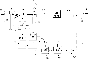
Make amplifier can reduce the influence of INTERMOD with more linear mode work.Utilize feedforward compensation can improve the linearity of amplifier.Fig. 1 shows feed-forward amplifier circuit 1.Feed-forward amplifier circuit 1 received RF input signal 11 also produces the radiofrequency signal 37 of amplifying through compensation.This feed-forward amplifier circuit 1 comprises first hybrid circuit 12, the first phase place micro actuator 14, delay circuit 18, radio-frequency power amplifier 20, the directional coupler 22 as detector, variable attenuator 24, second hybrid circuit 26, second variable attenuator 28, the second phase place micro actuator 30, amplifier 32, second delay circuit 34 and as second directional coupler 36 of synthesizer.
With reference to Fig. 2 a, there is shown a kind of frequency spectrum legend of input signal 11 of demonstration.According to this example, input signal 11 has two frequency components, and frequency is F1 and F2.Fig. 2 b shows available amplifying signal 21 after the input signal shown in Fig. 2 a 11 passes through power amplifier 20.Can see that amplifying signal 21 has three rank INTERMOD 21a and the 21b that frequency is respectively 2F1-F2 and 2F2-F1.These INTERMOD drop in the emission band of the transmitter that comprises this amplifying circuit usually.Circuit described in Fig. 1 is isolated by amplifier 20 and is incorporated into additional frequency component in the input signal 11 as error signal 27.Therefore, error signal 27 its frequency spectrums are the frequency spectrum that the frequency spectrum of the amplifying signal 21 shown in Fig. 2 b deducts the input signal 11 shown in Fig. 2 a in essence.Therefore its form of frequency spectrum of error signal 27 is similar to the form shown in Fig. 2 c.Therefore, be appreciated that, this error signal is to produce like this: obtain the sampling of input signal 11 and amplifying signal 21, and the relative phase and the amplitude relation of adjustment sampling, so that the non-distortion component in the amplifying signal 21 is eliminated, thereby the distortion component that keeps remaining amplifying signal 21 is as error signal 27.First and second hybrid circuits 12 and 26 introduce one and equal+180 ° phase shift.Phase place micro actuator 14 and delay circuit 18 are further introduced a variable phase shift, and this phase shift is used to compensate signal and the different delayed time between the signal that second input at second hybrid circuit that the first hybrid circuit input is imported receives in that the first input end at second hybrid circuit that first hybrid circuit is imported receives.
Refer again to Fig. 1, error signal 27 its power are adjusted through second variable attenuator 28.Then, the second phase place micro actuator 30 changes the phase place of error signal 27 with respect to amplifying signal 21.Then, this error signal is compensated error signal 33 through the buffering of amplifier 32.Second variable attenuator 28 receives second attenuation control signal 29 in its control input end, this control signal is used for the power level of control compensation error signal 33.The second phase place micro actuator 30 receives second phase control signal 31 in its control input end, this control signal is used for the phase place of the time-delay amplifying signal 35 that is produced with respect to second delay circuit of control compensation error signal 33.Compensating error signal 33 is input to second directional coupler 36 as synthesizer as input.Synthesizer 36 also receives time-delay amplifying signal 35.This synthesizer is coupled to time-delay amplifying signal 35 with compensating error signal 33, thereby is compensated amplifying signal 37, by 1 output of feedforward application circuit.
The purposes of second delay circuit 34, second variable attenuator 28, the second phase place micro actuator 30 and second amplifier 32 is, guarantee compensating error signal 33 and time-delay amplifying signal 35 in time by relevant and adjusting range, so that synthesizer 36 place's compensating error signals 33 can both be represented the synthesizer 36 places contained distorted signals in the amplifying signal 35 of delaying time at any time.Synthesizer 36 is synthetic with time-delay amplifying signal 35 with compensating error signal 33, eliminating this distortion basically from time-delay amplifying signal 35, thereby is compensated amplifying signal 37.
With reference to Fig. 2 c, there is shown the spectrogram of the compensating error signal 33 that obtains from input signal 11 with the frequency spectrum shown in Fig. 2 a and Fig. 2 b and amplifying signal 21.Fig. 2 d shows the frequency spectrum of resulting compensation amplifying signal 37 after compensating error signal shown in Fig. 2 c 33 and the time-delay amplifying signal 35 that gets from the amplifying signal 21 shown in Fig. 2 b synthesize.
Amplifying circuit 1 is worked well in order to feedover,, except producing 180 ° phase shift eliminating usefulness, must have and the identical electrical length of alternate path through the path of the cancellation loop of first hybrid circuit 12, first micro actuator 14, delay circuit 18 and second hybrid circuit 26 through the cancellation loop of first hybrid circuit 12, power amplifier 20, detector 22, first variable attenuator 24 and second hybrid circuit 26.In first path still the change of the electrical length of the arbitrary parts in the alternate path all can upset this condition and current elimination effect.Therefore, the change of the electrical length of the arbitrary parts in these two paths all should be compensated.This compensation realizes by first phase control signal 15.
Fig. 3 a shows a kind of first phase-control circuit 2 that is used to provide first phase control signal 15.This phase-control circuit comprises directional coupler 40, the directional coupler 42 as the 3rd detector, frequency mixer 44, the phase-locked loop (PLL) 46 as second detector.40 pairs of time-delays of second detector phase compensation signal 19 is sampled, and obtains second detection signal 41, and this signal is input to frequency mixer 44.42 pairs of decay of the 3rd detector detection signal 39 is sampled, and obtains the 3rd detection signal 43, and this signal also is input to frequency mixer 44.Frequency mixer 44 multiplies each other second detection signal 41 and the 3rd detection signal 43, obtains mixed frequency signal 45, and this signal is input to phase-locked loop 46.Phase-locked loop 46 produces first phase control signal 15.First phase control signal 15 has a value that depends on the phase difference between time-delay phase compensation signal 19 and the decay detection signal 39.This signal change first phase place micro actuator 14 and then change phase compensation signal 17 and time-delay phase compensation signal 19.Therefore, set up a feedback control loop that contains phase-locked loop, this loop can change the phase relation between time-delay phase compensation signal 19 and the decay detection signal 39, thereby makes first and second paths in the cancellation loop have identical electrical length.
The subject matter of first phase-control circuit 2 is, if mixed frequency signal 45 is multifrequency, phase-locked loop can not be worked well so.For multifrequency input term signal, the locking condition of phase-locked loop is stable inadequately.
Fig. 3 b shows second phase-control circuit 4 that can be used for addressing this problem.According to this solution, in input signal 11, introduce a pilot tone.This pilot tone is in the transmitter that comprises amplifying circuit 1 and sends outside the transmission band of signal.The effect of pilot tone is just in order to be lockable on the signal phase-locked loop 46.For this reason, pilot tone is introduced in the input signal 11, after a while by narrow band filter filtering from compensation amplifying signal 37.Usually, can adopt notch filter, this notch filter is used for the filtering pilot tone specially for this reason.Second phase-control circuit 4 is similar to first phase-control circuit 2, but it also has one first narrow band filter 48, be used for second detection signal 41 is carried out filtering and obtains the first narrow band detection signal 49, this signal is that a frequency that has with pilot tone is the signal of the narrow-band at center.This circuit also has one second narrow band filter 50, and being used for the 3rd detection signal 43 is carried out filtering and obtains a frequency that has with pilot tone is the second narrow band detection signal 51 of the narrow-band at center.Frequency mixer 44 is synthetic with the first narrow band detection signal 49 and the second narrow band detection signal 51, obtains a mixed frequency signal 45 that has with the pilot tone narrow-band that is the center.This signal is used for producing first phase control signal 15 by phase-locked loop.In addition, the working method of first phase-control circuit 2 among the circuit working mode among Fig. 3 b and Fig. 3 a is identical.The shortcoming of second phase-control circuit 4 is that pilot tone is outside the frequency band of amplifier, also outside the transmission band of the receiver that contains this application circuit.Therefore, the effect that does not guarantee 20 pairs of pilot tones of power amplifier is equal to the effect to the input signal 11 that finally is sent out after amplifying.Pilot tone still is a very big unwanted signal that needs additional components, therefore to strengthen filtering in case from compensation amplifying signal 37 this signal of filtering.In addition, also need to increase a synthesizer so that pilot tone is offered first hybrid circuit 12 at input.This synthesizer has certain volume, quality and power requirement, and must not be subjected to the influence of other parts of amplifier, otherwise may produce cross interference.Therefore, adopt second phase-control circuit 4 to provide the amplifying circuit of first phase control signal 15 also to have many problems.
The purpose of embodiments of the present invention provides a kind of modified model feedforward amplifying circuit.
According to an aspect of the present invention, a kind of feedforward amplifying circuit that is used to produce the compensation output signal is provided, it comprises: an amplifier, be used to receive the input signal that contains control signal in a plurality of predetermined bands, and producing the interior amplifying signal that contains described control signal of a plurality of described predetermined bands, wherein said predetermined band is in the working range of amplifier; Phase changer is used to receive described input signal and described amplifying signal, and introduces a relative phase shift between described input signal and described amplifying signal, to produce an error signal; Synthesizer is used for described error signal and described amplifying signal are synthesized, to produce described compensation output signal; And control device, be used for controlling described phase changer according to the control signal of described input signal and the relative phase difference between the control signal in the described amplifying signal.
Contrast with combining the described configuration of Fig. 3 b, the frequency of this control signal is in the working range of amplifier.The pilot tone of Fig. 3 b is not in the working range of amplifier.That is to say, compare, in embodiments of the present invention, can obtain better error compensation with the configuration among Fig. 3 b.In addition, in embodiments of the present invention, control signal preferably is used because of other reasons, and not just as a pilot signal.
Described control device preferably includes the first selectivity checkout gear that can select preset frequency, be used for detecting the control signal of described input signal, with the second selectivity checkout gear that can select described preset frequency, be used for detecting the control signal of described amplifying signal.The first and second selectivity checkout gears can be controlled, to change described preset frequency.The described first and second selectivity checkout gears preferably all comprise a tuned resonating cavity.Preset frequency can be in described predetermined band.Input unit can be used for receiving the signal that is used to control the described first and second selectivity checkout gears that is provided.
Synthesizer can also comprise phase place change device, is used to change the phase place of described error signal with respect to described amplifying signal.Phase place change device can be used for controlling described relative phase according to described control signal in the described amplifying signal and the relative phase difference between the described control signal in the described error signal.Phase place change device can comprise the 3rd selectivity checkout gear that can select preset frequency, be used for detecting the described control signal of described amplifying signal, with the 4th selectivity checkout gear that can select described preset frequency, be used for detecting the described control signal of described error signal.
The third and fourth selectivity checkout gear can be controlled, to select described preset frequency.The third and fourth selectivity checkout gear can comprise a tuned resonating cavity separately.Preset frequency can be in described predetermined band.Input unit can be used for receiving the signal that is used to control the described third and fourth selectivity checkout gear that is provided.
Described phase changer preferably can be used to described input signal and described amplifying signal synthetic, to produce described error signal.Error signal can be represented the weighted difference between described input signal and the described amplifying signal.This phase changer can also comprise attenuating device or amplifying device, is used for before described synthesizing described input signal and/or described amplifying signal weighting.This phase changer can also comprise time-delay mechanism, is used for introducing between described input signal and described amplifying signal before described synthesizing a fixing relative time delay.This phase changer can also comprise hybrid circuit, is used for receiving described input signal and a fixed phase drift is incorporated into described input signal.
Described phase changer preferably can also comprise a directional coupler that is connected the output of described amplifier, and wherein said directional coupler is coupled to described error signal in the described amplifying signal, to produce described compensation output signal.This phase changer can comprise hybrid circuit, is used for after introducing described relative phase shift described input signal and described amplifying signal is synthetic.Phase changer can comprise the phase place micro actuator, and it is introduced into the described relative phase shift of small part, and described phase place micro actuator receives the control input from described control device.Control device and phase changer preferably constitute a feedback control loop.
Described control device preferably also comprises phase-locked loop circuit.The most handy decay or amplifying device are decayed or are amplified described error signal.Phase place change device and error signal can constitute feedback control loop.Phase place change device can also comprise phase-locked loop circuit.
Base station in the cellular wireless networks preferably includes above described circuit, and the described output signal that wherein contains described control signal is sent by the base station.Therefore, this control signal has reached the inaccessiable purpose of pilot tone function.
If the base station is by GSM standard work, this control signal can send with Broadcast Control Channel (BCCH) so.Control signal in the described output signal constantly is sent out and/or has a constant power level and/or be used to discern the base station.
According to a second aspect of the invention, provide a kind of and be used to amplify radiofrequency signal so that the method for transmission, this method may further comprise the steps: receive the input signal that contains control signal in a plurality of predetermined bands; Amplify described input signal to produce the amplifying signal that contains described control signal in a plurality of described predetermined bands; Compensate described a plurality of amplifying signal eliminating the noise that described amplification procedure is brought, thereby produce the compensation amplifying signal that contains described control signal in a plurality of described predetermined bands; Contain the described compensation amplifying signal of described control signal with transmission, wherein said compensation process comprises: detect input signal and amplifying signal; Detecting input signal and detecting and introduce a phase shift between the amplifying signal, to produce an error signal; With described error signal and described amplifying signal is synthetic, to produce described compensation output signal.
In order to understand the present invention better and to understand the present invention and how to realize, describe below with reference to accompanying drawings, wherein:
Fig. 1 shows the feedforward amplifying circuit;
Fig. 2 a-2d shows the frequency spectrum of some signals shown in Fig. 1 when the input signal 11 of demonstration is input in the amplifying circuit;
Fig. 3 a shows a kind of existing apparatus that is used to provide first phase control signal 15;
A kind of existing apparatus that is used to provide first phase control signal 15 when Fig. 3 b shows outside adopting band pilot tone;
Fig. 4 show according to of the present invention in adopting band a kind of preferred embodiment that is used to provide first phase control signal 15 during pilot tone;
A kind of device that is used to provide second phase control signal 31 when Fig. 5 shows in adopting band pilot tone.
As previously described, the receiving terminal in the cellular communications network is served by specific base stations according to its position.Each sub-district can be used the communication channel different with its adjacent cell at any time.This has prevented the phase mutual interference.When transceiver terminal when a sub-district moves to another sub-district, which sub-district it need know it in, in other words, which communication channel it should should use with which base station communication and it.In case between transceiver terminal and base station, set up channel, just send the data (as voice or other information) that to communicate by letter between transceiver terminal and the base station with the communication channel set up.Therefore, send number control signal by the base station usually,, make transceiver terminal can discern immediate base station like this and it communicates used channel so that received by transceiver terminal.According to global mobile communication (GSM) standard, a kind of dedicated channel that is called Broadcast Control Channel (BCCH) has been adopted in the base station, so that communicate by letter with transceiver terminal.BCCH is by distributing transmission frequency and time slot, is used for controlling communicate by letter with transceiver terminal channel with transceiver terminal and base station communication of base station.BCCH also is the transceiver terminal specific base.With reference to Fig. 1, BCCH is the part of input signal 11 and is the part of compensation amplifying signal 37.It is one with the signal that is sent out, and need not filtering and just it can be eliminated from compensation amplifying signal 37.This BCCH signal constantly sends on all time slots and does not change the RF level.
The inventor has recognized that, utilizes the component of input signal 11 itself especially beneficial as pilot tone in Fig. 1.Like this, just can need not an independent synthesizer and obtain pilot tone, need not an independent filter and leach pilot tone the amplifying signal 37 from compensation, and mean pilot tone in the working range of amplifier and the receiver that is containing amplifying circuit 1 send in the frequency band of signal.In the enforcement transmitter of the present invention that carries out work according to GSM standard, can be with the BCCH signal as pilot tone.
The circuit that is suitable as the feedforward amplifying circuit has been shown among Fig. 1.The circuit that is used to provide first phase control signal 15 has been shown among Fig. 4.The consistent place of label among label in Fig. 4 and Fig. 3 b, identical signal or the parts of they expressions.Fig. 4 shows a kind of phase-control circuit 6, the difference of second phase-control circuit 4 among this circuit and Fig. 3 b is that first band pass filter 48 among Fig. 3 b and second band pass filter 50 replace with first variable filter 52 and second variable filter 54 respectively.
First and second variable filters can be tuned resonating cavities.Base stations control circuit 6 produces first phase control signal 15, and is described in conjunction with Fig. 3 a as the front, and this signal constitutes the part of the feedback control loop in the feed-forward amplifier circuit 1.
This compensation loop can be eliminated the distortion in synthesizer 36 that power amplifier 20 brings, and this loop has two independent paths.First path process itself has the cancellation loop of two paths, and then through second variable attenuator 28, the second phase place micro actuator 30, amplifier 32 and synthesizer 36.Alternate path is through first hybrid circuit 12, power amplifier 20, detector 22, delay circuit 34 and synthesizer 36.If eliminate in synthesizer 36 well, the electrical length of first and second paths of compensation loop should equate so.Under the control of second phase control signal 31, the second phase place micro actuator 30 can guarantee that two paths both electrical length except 180 ° phase shift eliminating usefulness in the compensation loop equate.The change of the electrical length of the arbitrary parts in these two paths all can be upset this condition, therefore will compensate by second phase control signal 31.
With reference to Fig. 5, there is shown the control circuit 8 that is used to provide second phase control signal 31.Control circuit 8 comprises directional coupler 60 as the 4th detector, the 3rd variable filter 62, as directional coupler 64, the 4th variable filter 66, second frequency mixer 68 and second phase-locked loop (PLL) of the 5th detector.The 3rd variable filter 62 and the 4th variable filter 66 be similar to shown in Fig. 4 and in conjunction with described first variable filter 52 of this figure and second variable filter 54.The 3rd variable filter and the 4th variable filter be receiving filter control signal 57 separately, and this control signal determines that third and fourth variable filter allows the frequency by them separately.
The 4th detector 60 detects time-delay amplifying signal 35, detects time-delay amplifying signal 61 to produce, and this signal is input to the 3rd variable filter.The narrow-band that the 3rd variable filter allows signal by it to produce the 3rd filtering signal 63.The 3rd filtering signal 63 comprises pilot tone, and in the GSM execution mode, the frequency of this pilot tone is on the BCCH Frequency point.The 5th detector 64 detects compensating error signal 33 and produces and detects compensating error signal 65, and this signal is input to the 4th variable filter 66.The 4th variable filter produces the 5th filtering signal 67, and this signal has a narrow-band that comprises the frequency of pilot tone, and in the GSM execution mode, this frequency is the BCCH frequency.Third and fourth filtering signal 63 and 67 is input in second frequency mixer 68 as input, and frequency mixer 68 produces second mixed frequency signal 69, and this signal is input to second phase-locked loop 70.Second phase-locked loop 70 produces second phase control signal 31.
With reference to Fig. 1, second phase control signal, 31 control compensation error signals 33.Therefore, control circuit 8, the second phase place micro actuator 30 and compensating error signal 33 are united the formation feedback circuit, this circuit makes i.e. 180 ° the not homophase of the suitable correlation of the electrical length maintenance of first and second paths in the compensation loop, like this, after compensating error signal 33 and time-delay amplifying signal 35 are synthesized, can produce a compensation amplifying signal 37 that is not subjected to the influence of amplifier 20 caused distortions basically.Should be appreciated that pilot tone is significantly less than pilot tone to time-delay amplifying signal 35 roles to compensating error signal 33 roles.Therefore, the 4th filtering signal 67 is more much smaller than the amplitude of the 3rd filtering signal 63 usually, and the characteristic of frequency mixer 68 must be selected, and like this, second mixed frequency signal 69 can have suitable characteristic, so that lockable second phase-locked loop 70.
Embodiments of the present invention can be incorporated in portable terminal.
Although abovely described embodiments of the present invention in conjunction with gsm system, yet embodiments of the present invention suitable can send the channel of two different frequencies and one of them channel is unifrequent fdma system simultaneously applicable to any other.
Although abovely described embodiments of the present invention in conjunction with transceiver, yet, should be appreciated that embodiments of the present invention also can have widely to use that it can be applicable to the aspect that any other suitable needs feedforward is amplified.
Claims (38)
1. one kind is used to produce the feedforward amplifying circuit that compensates output signal, and it comprises:
An amplifier is used to receive the input signal that contains control signal in a plurality of predetermined bands, and produces the amplifying signal that contains described control signal in a plurality of described predetermined bands, and wherein said predetermined band is in the working range of amplifier;
Phase changer is used to receive described input signal and described amplifying signal, and introduces a relative phase shift between described input signal and described amplifying signal, to produce an error signal;
Synthesizer is used for described error signal and described amplifying signal are synthesized, to produce described compensation output signal; With
Control device is used for controlling described phase changer according to the control signal of described input signal and the relative phase difference between the control signal in the described amplifying signal.
2. circuit as claimed in claim 1, wherein, described control device comprises the first selectivity checkout gear that can select preset frequency, be used for detecting the control signal of described input signal, with the second selectivity checkout gear that can select described preset frequency, be used for detecting the control signal of described amplifying signal.
3. circuit as claimed in claim 2, wherein, the described first and second selectivity checkout gears are controlled, to change described preset frequency.
4. as claim 2 or 3 described circuit, wherein, the described first and second selectivity checkout gears all comprise a tuned resonating cavity.
5. as claim 2,3 or 4 described circuit, wherein, described preset frequency is in described predetermined band.
6. circuit as claimed in claim 5 also comprises input unit, is used for receiving the signal that is used to control the described first and second selectivity checkout gears that is provided.
7. as the arbitrary described circuit of above-mentioned claim, wherein, described synthesizer also comprises phase place change device, is used to change the phase place of described error signal with respect to described amplifying signal.
8. circuit as claimed in claim 7, wherein, described phase place change device is used for controlling described relative phase according to described control signal in the described amplifying signal and the relative phase difference between the described control signal in the described error signal.
9. circuit as claimed in claim 8, wherein, described phase place change device comprises the 3rd selectivity checkout gear that can select preset frequency, be used for detecting the described control signal of described amplifying signal, with the 4th selectivity checkout gear that can select described preset frequency, be used for detecting the described control signal of described error signal.
10. circuit as claimed in claim 9, wherein, the described third and fourth selectivity checkout gear is controlled, to select described preset frequency.
11. as claim 9 or 10 arbitrary described circuit, wherein, the described third and fourth selectivity checkout gear comprises a tuned resonating cavity separately.
12. as claim 9,10 or 11 described circuit, wherein, described preset frequency is in described predetermined band.
13. circuit as claimed in claim 12 also comprises input unit, is used for receiving the signal that is used to control the described third and fourth selectivity checkout gear that is provided.
14. as the arbitrary described circuit of above-mentioned claim, wherein, described phase changer is used for described input signal and described amplifying signal synthetic, to produce described error signal.
15. circuit as claimed in claim 14, wherein, described error signal is represented the weighted difference between described input signal and the described amplifying signal.
16. as claim 14 or 15 described circuit, wherein, described phase changer also comprises attenuating device or amplifying device, is used for before described synthesizing described input signal and/or described amplifying signal weighting.
17. as claim 14,15 or 16 described circuit, wherein, described phase changer also comprises time-delay mechanism, is used for introducing between described input signal and described amplifying signal before described synthesizing a fixing relative time delay.
18. as the arbitrary described circuit of claim 14-17, wherein, described phase changer also comprises hybrid circuit, is used for receiving described input signal and a fixed phase drift is incorporated into described input signal.
19. as the arbitrary described circuit of above-mentioned claim, wherein, described phase changer also comprises a directional coupler that is connected the output of described amplifier, and wherein said directional coupler is coupled to described error signal in the described amplifying signal, to produce described compensation output signal.
20. as claim 14 or the above-mentioned described circuit of arbitrary claim that depends on claim 14, wherein, described phase changer comprises hybrid circuit, is used for after introducing described relative phase shift described input signal and described amplifying signal is synthetic.
21. as claim 14 or the above-mentioned described circuit of arbitrary claim that depends on claim 14, wherein, described phase changer comprises the phase place micro actuator, and it is introduced into the described relative phase shift of small part, and described phase place micro actuator receives the control input from described control device.
22. as the arbitrary described circuit of above-mentioned claim, wherein, described control device and phase changer constitute a feedback control loop.
23. as the arbitrary described circuit of above-mentioned claim, wherein, described control device also comprises phase-locked loop circuit.
24. as the arbitrary described circuit of above-mentioned claim, wherein, with decaying or amplifying device is decayed or amplified described error signal.
25. as claim 7 or the above-mentioned described circuit of arbitrary claim that depends on claim 7, wherein, described phase place change device and error signal constitute feedback control loop.
26. as claim 7 or the above-mentioned described circuit of arbitrary claim that depends on claim 7, wherein, described phase place change device also comprises phase-locked loop circuit.
27. the base station in the cellular wireless networks comprises arbitrary described circuit in the aforesaid right requirement, wherein, the described output signal that contains described control signal is sent by the base station.
28. base station as claimed in claim 27, this base station is by GSM standard work, and wherein, described control signal sends with Broadcast Control Channel (BCCH).
29. as depend on and the claim 27 or the 28 described base stations of claim 3 or 10 comprise the circuit that is used to control described first and second selectivity checkout gears and/or the described third and fourth selectivity checkout gear.
30. Cellular Networks, comprise a plurality of as claim 27,28 or 29 described base stations and a plurality of receiving terminal, wherein, the described control signal in the described output control signal constantly is sent out and/or has a constant power level and/or be used to discern the base station.
31. a transceiver comprises arbitrary described circuit among the claim 1-26.
32. one kind be used to amplify radiofrequency signal in case the transmission method, this method may further comprise the steps:
Receive a plurality of input signals that contain control signal in the predetermined band;
Amplify described input signal to produce a plurality of amplifying signals that contain described control signal in the described predetermined band;
Compensate described a plurality of amplifying signal eliminating the noise that described amplification procedure is brought, thereby produce the compensation amplifying signal that contains described control signal in a plurality of described predetermined bands; With
Transmission contains the described compensation amplifying signal of described control signal, and wherein said compensation process comprises:
Detect input signal and amplifying signal;
Detecting input signal and detecting and introduce a phase shift between the amplifying signal, to produce an error signal; With
Described error signal and described amplifying signal is synthetic, to produce described compensation output signal.
33. method as claimed in claim 32, wherein, described compensation process is introduced a variable power before also being included in and producing described error signal between described detection input and amplifying signal.
34. as claim 32 or 33 described methods, wherein, describedly detect that the step of the phase difference between control signal and the control signal of detect in the amplifying signal in the input signal detects in institute and the step in the step formation feedback control loop of introducing phase difference between described detection input signal and detection amplifying signal, wherein, detect in the input signal control signal and the detection of the phase difference between the control signal in the amplifying signal of detecting just carry out after between the two, having introduced phase difference.
35. as arbitrary described method among the claim 32-34, wherein, describedly introduce phase difference between the amplifying signal and may further comprise the steps with detecting detecting input signal: a phase difference is incorporated into detects among arbitrary in input signal or the detection amplifying signal with the step that produces error signal, then that these signals are synthetic to produce described error signal, the change of wherein said phase place can Be Controlled, make, in described error signal, can eliminate control signal that detects in the input signal and the control signal that detects in the amplifying signal basically.
36. as arbitrary described method among the claim 32-35, wherein, the described step that error signal and described amplifying signal is synthetic comprises power attenuation or amplification procedure.
37. as arbitrary described method among the claim 32-36, wherein, the described step that error signal and described amplifying signal is synthetic also is included in and introduces a phase place change with respect to described amplifying signal in the described error signal.
38. method as claimed in claim 37, wherein, in described error signal, introduce the part that a step with respect to the phase place change of described output signal constitutes feedback control loop, this feedback control loop comprises, between described error signal and described amplifying signal, introduce after the described phase place change, detect the phase difference between described amplifying signal and the described error signal.
Applications Claiming Priority (2)
| Application Number | Priority Date | Filing Date | Title |
|---|---|---|---|
| GB9814400.9 | 1998-07-02 | ||
| GBGB9814400.9A GB9814400D0 (en) | 1998-07-02 | 1998-07-02 | Amplifier circuitry |
Publications (1)
| Publication Number | Publication Date |
|---|---|
| CN1307746A true CN1307746A (en) | 2001-08-08 |
Family
ID=10834867
Family Applications (1)
| Application Number | Title | Priority Date | Filing Date |
|---|---|---|---|
| CN99808115A Pending CN1307746A (en) | 1998-07-02 | 1999-07-01 | Amplifier circuitry |
Country Status (8)
| Country | Link |
|---|---|
| US (1) | US6836671B2 (en) |
| EP (1) | EP1125361A1 (en) |
| JP (1) | JP2002520893A (en) |
| CN (1) | CN1307746A (en) |
| AU (1) | AU4780399A (en) |
| GB (1) | GB9814400D0 (en) |
| NO (1) | NO20006602L (en) |
| WO (1) | WO2000002308A1 (en) |
Cited By (1)
| Publication number | Priority date | Publication date | Assignee | Title |
|---|---|---|---|---|
| CN1833365B (en) * | 2003-08-05 | 2011-09-14 | 摩托罗拉移动公司 | Apparatus and method for transmitter phase shift compensation |
Families Citing this family (49)
| Publication number | Priority date | Publication date | Assignee | Title |
|---|---|---|---|---|
| US6697611B1 (en) * | 2000-11-14 | 2004-02-24 | Intel Corporation | Method and apparatus for performing DC offset cancellation in a receiver |
| US20050200422A1 (en) * | 2001-09-20 | 2005-09-15 | Khosro Shamsaifar | Tunable filters having variable bandwidth and variable delay |
| US7058368B2 (en) * | 2002-06-27 | 2006-06-06 | Nortel Networks Limited | Adaptive feedforward noise cancellation circuit |
| US6850115B2 (en) * | 2002-08-26 | 2005-02-01 | Powerwave Technologies, Inc. | Enhanced efficiency LDMOS based feed forward amplifier |
| DE10244511A1 (en) * | 2002-09-25 | 2004-04-15 | Mahle Gmbh | Multi-part cooled piston for an internal combustion engine |
| US7123086B2 (en) * | 2003-05-07 | 2006-10-17 | Powerwave Technologies, Inc. | Feed forward amplifier employing positive feedback pilot generation |
| CA2509707A1 (en) * | 2004-06-10 | 2005-12-10 | Andre Gagnon | Apparatus and method for tracing a path travelled by an entity or object, and tag for use therewith |
| US7308234B2 (en) * | 2005-01-19 | 2007-12-11 | Northrop Grumman Corporation | Feedforward spur cancellation approach using low IP amplifier |
| US8784336B2 (en) | 2005-08-24 | 2014-07-22 | C. R. Bard, Inc. | Stylet apparatuses and methods of manufacture |
| US7856464B2 (en) * | 2006-02-16 | 2010-12-21 | Sigmatel, Inc. | Decimation filter |
| US8388546B2 (en) | 2006-10-23 | 2013-03-05 | Bard Access Systems, Inc. | Method of locating the tip of a central venous catheter |
| US7794407B2 (en) | 2006-10-23 | 2010-09-14 | Bard Access Systems, Inc. | Method of locating the tip of a central venous catheter |
| CN101119121B (en) * | 2007-08-21 | 2010-08-25 | 华为技术有限公司 | Anti-interference method in receiver, anti-interference receiver and anti-interference device |
| JP5452500B2 (en) | 2007-11-26 | 2014-03-26 | シー・アール・バード・インコーポレーテッド | Integrated system for intravascular placement of catheters |
| US10524691B2 (en) | 2007-11-26 | 2020-01-07 | C. R. Bard, Inc. | Needle assembly including an aligned magnetic element |
| US9649048B2 (en) | 2007-11-26 | 2017-05-16 | C. R. Bard, Inc. | Systems and methods for breaching a sterile field for intravascular placement of a catheter |
| US8849382B2 (en) | 2007-11-26 | 2014-09-30 | C. R. Bard, Inc. | Apparatus and display methods relating to intravascular placement of a catheter |
| US10449330B2 (en) | 2007-11-26 | 2019-10-22 | C. R. Bard, Inc. | Magnetic element-equipped needle assemblies |
| US8781555B2 (en) | 2007-11-26 | 2014-07-15 | C. R. Bard, Inc. | System for placement of a catheter including a signal-generating stylet |
| US10751509B2 (en) | 2007-11-26 | 2020-08-25 | C. R. Bard, Inc. | Iconic representations for guidance of an indwelling medical device |
| US9521961B2 (en) | 2007-11-26 | 2016-12-20 | C. R. Bard, Inc. | Systems and methods for guiding a medical instrument |
| US9456766B2 (en) | 2007-11-26 | 2016-10-04 | C. R. Bard, Inc. | Apparatus for use with needle insertion guidance system |
| US8478382B2 (en) | 2008-02-11 | 2013-07-02 | C. R. Bard, Inc. | Systems and methods for positioning a catheter |
| US9901714B2 (en) | 2008-08-22 | 2018-02-27 | C. R. Bard, Inc. | Catheter assembly including ECG sensor and magnetic assemblies |
| US8437833B2 (en) | 2008-10-07 | 2013-05-07 | Bard Access Systems, Inc. | Percutaneous magnetic gastrostomy |
| US8965454B2 (en) * | 2009-03-04 | 2015-02-24 | Andrew Llc | Amplifier system for cell sites and other suitable applications |
| US9532724B2 (en) | 2009-06-12 | 2017-01-03 | Bard Access Systems, Inc. | Apparatus and method for catheter navigation using endovascular energy mapping |
| JP5795576B2 (en) | 2009-06-12 | 2015-10-14 | バード・アクセス・システムズ,インコーポレーテッド | Method of operating a computer-based medical device that uses an electrocardiogram (ECG) signal to position an intravascular device in or near the heart |
| WO2011019760A2 (en) | 2009-08-10 | 2011-02-17 | Romedex International Srl | Devices and methods for endovascular electrography |
| EP2517622A3 (en) | 2009-09-29 | 2013-04-24 | C. R. Bard, Inc. | Stylets for use with apparatus for intravascular placement of a catheter |
| WO2011044421A1 (en) | 2009-10-08 | 2011-04-14 | C. R. Bard, Inc. | Spacers for use with an ultrasound probe |
| BR112012019354B1 (en) | 2010-02-02 | 2021-09-08 | C.R.Bard, Inc | METHOD FOR LOCATION OF AN IMPLANTABLE MEDICAL DEVICE |
| CA2800813C (en) | 2010-05-28 | 2019-10-29 | C.R. Bard, Inc. | Apparatus for use with needle insertion guidance system |
| AU2011289513B2 (en) | 2010-08-09 | 2014-05-29 | C.R. Bard, Inc. | Support and cover structures for an ultrasound probe head |
| WO2012024577A2 (en) | 2010-08-20 | 2012-02-23 | C.R. Bard, Inc. | Reconfirmation of ecg-assisted catheter tip placement |
| WO2012058461A1 (en) | 2010-10-29 | 2012-05-03 | C.R.Bard, Inc. | Bioimpedance-assisted placement of a medical device |
| CN105662402B (en) | 2011-07-06 | 2019-06-18 | C·R·巴德股份有限公司 | Needle length for being inserted into guidance system is determining and calibrates |
| USD724745S1 (en) | 2011-08-09 | 2015-03-17 | C. R. Bard, Inc. | Cap for an ultrasound probe |
| USD699359S1 (en) | 2011-08-09 | 2014-02-11 | C. R. Bard, Inc. | Ultrasound probe head |
| US9211107B2 (en) | 2011-11-07 | 2015-12-15 | C. R. Bard, Inc. | Ruggedized ultrasound hydrogel insert |
| CN104837413B (en) | 2012-06-15 | 2018-09-11 | C·R·巴德股份有限公司 | Detect the device and method of removable cap on ultrasonic detector |
| US9214968B2 (en) * | 2013-07-24 | 2015-12-15 | Nokia Technologies Oy | Apparatus and methods for providing a power amplifier with interference cancellation |
| ES2811323T3 (en) | 2014-02-06 | 2021-03-11 | Bard Inc C R | Systems for the guidance and placement of an intravascular device |
| US9331735B1 (en) * | 2014-05-22 | 2016-05-03 | Hrl Laboratories, Llc | GaN based active cancellation circuit for high power simultaneous transmit and receive systems |
| US10973584B2 (en) | 2015-01-19 | 2021-04-13 | Bard Access Systems, Inc. | Device and method for vascular access |
| WO2016210325A1 (en) | 2015-06-26 | 2016-12-29 | C.R. Bard, Inc. | Connector interface for ecg-based catheter positioning system |
| US11000207B2 (en) | 2016-01-29 | 2021-05-11 | C. R. Bard, Inc. | Multiple coil system for tracking a medical device |
| US9837966B1 (en) * | 2016-08-26 | 2017-12-05 | Nxp Usa, Inc. | Series-type Doherty amplifier |
| EP3852622A1 (en) | 2018-10-16 | 2021-07-28 | Bard Access Systems, Inc. | Safety-equipped connection systems and methods thereof for establishing electrical connections |
Family Cites Families (6)
| Publication number | Priority date | Publication date | Assignee | Title |
|---|---|---|---|---|
| US5023565A (en) * | 1990-01-26 | 1991-06-11 | At&T Bell Laboratories | Linear amplifier with automatic adjustment of feed forward loop gain and phase |
| GB2254505B (en) * | 1990-04-25 | 1993-05-05 | British Tech Group | Apparatus and method for reducing distortion in amplification |
| US5077532A (en) * | 1990-12-17 | 1991-12-31 | Motorola, Inc. | Feed forward distortion minimization circuit |
| GB2273622A (en) * | 1992-12-15 | 1994-06-22 | British Tech Group | Spread spectrum pilot tone for distortion or instability correction |
| US5386198A (en) * | 1993-01-28 | 1995-01-31 | Telefonaktiebolaget L M Ericsson | Linear amplifier control |
| DE69422988T4 (en) * | 1994-12-21 | 2001-08-23 | Nec Corp | Feedforward amplifier |
-
1998
- 1998-07-02 GB GBGB9814400.9A patent/GB9814400D0/en not_active Ceased
-
1999
- 1999-07-01 JP JP2000558603A patent/JP2002520893A/en active Pending
- 1999-07-01 CN CN99808115A patent/CN1307746A/en active Pending
- 1999-07-01 WO PCT/EP1999/004536 patent/WO2000002308A1/en not_active Application Discontinuation
- 1999-07-01 AU AU47803/99A patent/AU4780399A/en not_active Abandoned
- 1999-07-01 EP EP99931227A patent/EP1125361A1/en not_active Withdrawn
-
2000
- 2000-12-13 US US09/739,030 patent/US6836671B2/en not_active Expired - Fee Related
- 2000-12-22 NO NO20006602A patent/NO20006602L/en not_active Application Discontinuation
Cited By (1)
| Publication number | Priority date | Publication date | Assignee | Title |
|---|---|---|---|---|
| CN1833365B (en) * | 2003-08-05 | 2011-09-14 | 摩托罗拉移动公司 | Apparatus and method for transmitter phase shift compensation |
Also Published As
| Publication number | Publication date |
|---|---|
| NO20006602L (en) | 2001-02-28 |
| US20020125948A1 (en) | 2002-09-12 |
| GB9814400D0 (en) | 1998-09-02 |
| US6836671B2 (en) | 2004-12-28 |
| AU4780399A (en) | 2000-01-24 |
| JP2002520893A (en) | 2002-07-09 |
| EP1125361A1 (en) | 2001-08-22 |
| NO20006602D0 (en) | 2000-12-22 |
| WO2000002308A1 (en) | 2000-01-13 |
Similar Documents
| Publication | Publication Date | Title |
|---|---|---|
| CN1307746A (en) | Amplifier circuitry | |
| EP0704986B1 (en) | CDMA cellular communications with multicarrier signal processing | |
| EP0704983B1 (en) | Method and apparatus for processing multicarrier signals | |
| US5212826A (en) | Apparatus and method of dc offset correction for a receiver | |
| EP0619656B1 (en) | Time division multiplex transmitting/receiving system | |
| US5752170A (en) | Transmitters for radio telephone base stations | |
| US6389269B1 (en) | Method and apparatus for multiple band transmission | |
| JP2000505263A (en) | Variable band repeater | |
| US5625871A (en) | Cellular communications system with multicarrier signal processing | |
| EP0704982B1 (en) | A radio receiver for processing a multi-carrier signal with a large dynamic range | |
| CN1781259A (en) | Full duplex multimode transceiver | |
| CN1354909A (en) | Frequency multiplex transmitter and method for emliminating crosstalk | |
| US7383025B2 (en) | Method for processing RF signals for receiving and transmission | |
| US7295820B2 (en) | Method and apparatus for DC offset control | |
| US6924716B2 (en) | Method and apparatus for reduction of electromagnetic feed through in a SAW filter | |
| EP1235344A2 (en) | Method for reducing interference in a transmitter | |
| JPH07264082A (en) | Distortion compensation device in radio transmitter | |
| US20040198266A1 (en) | Control circuitry | |
| KR20030018985A (en) | IMD eliminating equipment of the terminal system | |
| KR20020051662A (en) | Method of Forward Automatic Gaincontrol in Multi Carrier Radio Transmission |
Legal Events
| Date | Code | Title | Description |
|---|---|---|---|
| C06 | Publication | ||
| PB01 | Publication | ||
| C10 | Entry into substantive examination | ||
| SE01 | Entry into force of request for substantive examination | ||
| C02 | Deemed withdrawal of patent application after publication (patent law 2001) | ||
| WD01 | Invention patent application deemed withdrawn after publication |