CN1306547C - Plasma indicating panel - Google Patents
Plasma indicating panel Download PDFInfo
- Publication number
- CN1306547C CN1306547C CNB021412030A CN02141203A CN1306547C CN 1306547 C CN1306547 C CN 1306547C CN B021412030 A CNB021412030 A CN B021412030A CN 02141203 A CN02141203 A CN 02141203A CN 1306547 C CN1306547 C CN 1306547C
- Authority
- CN
- China
- Prior art keywords
- discharge
- electrode
- region
- display panel
- plasma display
- Prior art date
- Legal status (The legal status is an assumption and is not a legal conclusion. Google has not performed a legal analysis and makes no representation as to the accuracy of the status listed.)
- Expired - Fee Related
Links
Images


Classifications
-
- H—ELECTRICITY
- H01—ELECTRIC ELEMENTS
- H01J—ELECTRIC DISCHARGE TUBES OR DISCHARGE LAMPS
- H01J11/00—Gas-filled discharge tubes with alternating current induction of the discharge, e.g. alternating current plasma display panels [AC-PDP]; Gas-filled discharge tubes without any main electrode inside the vessel; Gas-filled discharge tubes with at least one main electrode outside the vessel
- H01J11/20—Constructional details
- H01J11/34—Vessels, containers or parts thereof, e.g. substrates
- H01J11/36—Spacers, barriers, ribs, partitions or the like
-
- H—ELECTRICITY
- H01—ELECTRIC ELEMENTS
- H01J—ELECTRIC DISCHARGE TUBES OR DISCHARGE LAMPS
- H01J11/00—Gas-filled discharge tubes with alternating current induction of the discharge, e.g. alternating current plasma display panels [AC-PDP]; Gas-filled discharge tubes without any main electrode inside the vessel; Gas-filled discharge tubes with at least one main electrode outside the vessel
- H01J11/10—AC-PDPs with at least one main electrode being out of contact with the plasma
- H01J11/12—AC-PDPs with at least one main electrode being out of contact with the plasma with main electrodes provided on both sides of the discharge space
-
- H—ELECTRICITY
- H01—ELECTRIC ELEMENTS
- H01J—ELECTRIC DISCHARGE TUBES OR DISCHARGE LAMPS
- H01J11/00—Gas-filled discharge tubes with alternating current induction of the discharge, e.g. alternating current plasma display panels [AC-PDP]; Gas-filled discharge tubes without any main electrode inside the vessel; Gas-filled discharge tubes with at least one main electrode outside the vessel
- H01J11/20—Constructional details
- H01J11/22—Electrodes, e.g. special shape, material or configuration
- H01J11/24—Sustain electrodes or scan electrodes
-
- H—ELECTRICITY
- H01—ELECTRIC ELEMENTS
- H01J—ELECTRIC DISCHARGE TUBES OR DISCHARGE LAMPS
- H01J11/00—Gas-filled discharge tubes with alternating current induction of the discharge, e.g. alternating current plasma display panels [AC-PDP]; Gas-filled discharge tubes without any main electrode inside the vessel; Gas-filled discharge tubes with at least one main electrode outside the vessel
- H01J11/20—Constructional details
- H01J11/34—Vessels, containers or parts thereof, e.g. substrates
- H01J11/38—Dielectric or insulating layers
Abstract
In a plasma display panel, a partition wall 15 surrounds each of discharge cells to define the discharge cells. Each of the discharge cells is divided by a second transverse wall 15B into a display discharge cell C1 which is opposite transparent electrodes Xa, Ya of paired row electrodes X, Y to provide for a sustaining discharge; and an addressing discharge cell C2 which is opposite a bus electrode Yb of the row electrode Y to provide for an addressing discharge caused between the bus electrode Yb and a column electrode D. A clearance r is provided between the discharge cell C1 and the addressing discharge cell C2 for communication between the cells C1 and C2.
Description
Technical field
The present invention relates to a kind of surface discharge type AC plasma display plate.
The present invention requires to enjoy the priority of Japanese 2001-213846,2001-218297 and 2002-13320 number application, and their disclosed contents are incorporated herein with for referencial use.
Background technology
In recent years, the surface discharge type AC plasma display plate has caused people's attention as a kind of elongated and large-scale color/graphics display, and has begun generally to be used for occasions such as general family.
Figure 34 to Figure 36 is a kind of schematic diagram of surface discharge type AC plasma display plate of traditional structure.Figure 34 is the front view of this traditional surface discharge type AC plasma display plate.Figure 35 is the cutaway view of being got along the V-V line among Figure 34.Figure 36 is the cutaway view of being got along the line W-W among Figure 34.
In Figure 34 to 36; this plasma display panel (hereinafter referred to as " PDP ") comprises the front glass substrate 1 as the PDP display surface; its back side be provided with successively a plurality of column electrodes to (X '; Y '), cover the protective layer 3 that dielectric layer 2 back sides were made and covered to column electrode to the dielectric layer 2 and the MgO of (X ', Y ').
Each column electrode to (X ', Y ') column electrode X ' and column electrode Y ' are respectively by transparency electrode Xa ', Ya ' and bus electrode Xb ', Yb ' constitutes, each transparency electrode is formed by the broad nesa coating that ITO etc. makes, and each bus electrode is formed by the narrower metal film that improves corresponding transparency electrode conductivity.
Column electrode X ' and Y ' alternately arrange on column direction, each to the electrode X ' of (X ', Y ') and Y ' at interval a discharging gap g ' face mutually.Column electrode forms a display line (OK) L to each column electrode in (X ', Y ') in matrix shows.
In each display line L, partition 5 is partitioned into a plurality of zones with discharge space S ', each zone corresponding to row electrode D ' and column electrode to (X ', Y ') crosspoint, these a plurality of zones are in order to limit discharge cell (dischage cell) C ', and these discharge cells C ' is the unit light-emitting zone.
This surface discharge type AC type PDP produces image by following program.
At first, in the addressing period after carrying out the reset cycle of reset discharge, column electrode is to causing discharge (address discharge) selectively between the electrode (being column electrode Y ' in this example) of (X ', Y ') and the row electrode D ' in each discharge cell C '.Because address discharge, make luminescence unit (wherein at the discharge cell that forms a wall electric charge (wall charge) on the dielectric layer 2) not luminescence unit (wherein at the discharge cell that does not form a wall electric charge on the dielectric layer 2) according to the image distribution that will show on the plate surface.
After finishing addressing period, a discharge sustain pulse alternately is added to simultaneously on each column electrode among each display line L right the column electrode X ' and Y '.Apply this discharge sustain pulse each time, just in each luminescence unit, cause continuous discharge between column electrode X ' and the Y ' by being formed at wall electric charge on the dielectric layer 2.
Continuous discharge in each luminescence unit causes producing the contained xenon ultraviolet ray in discharge gas.Red (R) among ultraviolet ray excited each the luminescence unit C ' that produces, green (G) or blue (B) fluorescence coating 6 form a display image thus.
In this traditional three-electrode surface discharge formula AC type PDP as mentioned above, in same discharge cell C ', produce address discharge and continuous discharge.Therefore, in each discharge cell C ', be inserted with in the middle of address discharge starts between the electrode of red (R), green (G) or blue (B) fluorescence coating 6, fluorescence coating 6 is used for sending color when causing continuous discharge.
For this reason, the address discharge that produces among the discharge cell C ' is subjected to the influence of fluorescence coating 6, and for example discharge performance becomes with the fluorescent material of all kinds that forms fluorescence coating 6, always change or the like when each layer thickness that produces when manufacture process forms fluorescence coating 6.Therefore, traditional PDP is difficult in and obtains identical address discharge characteristic among each discharge cell C '.
In aforesaid three-electrode surface discharge formula AC type PDP, a big discharge space need be arranged, in each discharge cell C ' in order to improve luminous efficiency.Therefore, prior art adopts the method that increases partition 5 height.
But,, produce the column electrode Y ' of address discharge and the interval between the row electrode D ' so therebetween and also increase if increase the height of partition 5 in order to improve luminous efficiency.The interval of this increase produces the problem that the used starting voltage of address discharge increases.
In addition, in aforementioned three-electrode surface discharge formula AC type PDP, for example increase more than 10%, can improve the luminous efficiency of PDP by xenon content in the discharge gas that will fill discharge space S '.But, if increase xenon content in the discharge gas, also increased the driving voltage that is used for address discharge and continuous discharge, cause producing the problem that the PDP electrical power consumed increases.
Summary of the invention
The present invention is in order to solve as mentioned above and the relevant problem of conventional surface discharge type AC plasma display plate.
Therefore, first purpose of the present invention is to provide a kind of surface discharge type AC plasma display plate, and it can stablize the address discharge performance in each discharge cell, and can improve luminous efficiency.
Except this first purpose, second purpose of the present invention is to provide a kind of surface discharge type AC plasma display plate, and it can reduce the driving voltage of address discharge and continuous discharge.
In order to reach first purpose, in accordance with a first feature of the invention, a kind of plasma display panel comprises: substrate before; A plurality of column electrodes are right, and on the back side of substrate, each extends and form a display line along a line direction before being arranged in along a column direction; One dielectric layer, the column electrode before covering on the substrate back is right; One meron, there is a discharge space on the opposite of substrate before placing between two substrates; A plurality of row electrodes, be arranged on that surface of meron of preceding substrate along this line direction, each row electrode along column direction extend with column electrode to intersecting, in the discharge space at each place, crosspoint, form the unit light-emitting zone, this plasma display panel comprises: partition, surround each unit light-emitting zone to limit the unit light-emitting zone; One partition wall, be used for each unit light-emitting zone is divided into first region of discharge and second region of discharge, discharge is faced and be used for producing to the relative part of each column electrode that first region of discharge is right with constituting each column electrode mutually between relative column electrode, second region of discharge is faced a part of uniting a column electrode in the column electrode that begins to discharge with the row electrode, and, between the part of row electrode and this column electrode, produce discharge; With a communication means, be arranged between first region of discharge and second region of discharge, it is communicated to first region of discharge from second region of discharge.
Have in the plasma display panel of first feature, when producing image, in second region of discharge (addressing discharge cell) that in the unit light-emitting zone that partition wall separates, forms, between a column electrode of row electrode and each column electrode centering of formation, cause discharge (address discharge).By being arranged on the communication means between first and second region of discharges, the discharge that causes in second region of discharge is transferred to first region of discharge, and is diffused in first region of discharge.The image distribution that first region of discharge (the not having luminescence unit) basis that like this, wherein is formed with first region of discharge (luminescence unit) of a wall electric charge and does not wherein have the wall electric charge to form will produce is on the plate surface.
Afterwards, be formed with therein in each first region of discharge (luminescence unit) of wall electric charge, each column electrode right at each column electrode of formation causes another discharge between the part relatively.The ultraviolet ray excited fluorescence coating that is used to launch the primary colors red (R) of colourama, green (G) and blue (B) that continuous discharge produced forms image with the response image signal on the plate surface.
According to first feature, in this manner, for the unit light-emitting zone that will wherein be formed with the wall electric charge and the unit light-emitting zone that wherein do not have the wall electric charge to form are assigned on the plate surface, in second region of discharge, produce address discharge between row electrode and each column electrode of column electrode centering, after finishing address discharge, second region of discharge is formed at and constitutes between the right column electrode of each column electrode so that luminous, and this is irrelevant with first region of discharge that wherein produces continuous discharge.For this reason, even design the discharge space of first region of discharge bigger to improve the luminous efficiency of plasma display panel, and, increase column electrode and row distance between electrodes thus, also the row electrode can be placed position, in order to reduce the starting voltage between row electrode and the column electrode than its more close second region of discharge in position at first region of discharge.The starting voltage that has improved luminous efficiency like this, simultaneously and reduced between row electrode and column electrode, to discharge.
In addition, independent design is used for being expert at and produces first region of discharge of discharge and be used for producing second region of discharge of discharge between row electrode and column electrode between the column electrode of electrode pair, need not to form in second region of discharge fluorescence coating by Discharge illuminating.The discharge that produces between row electrode and the column electrode in second region of discharge is not formed the influence of the color of fluorescent material and the fluorescence coating varied in thickness of fluorescence coating, thereby provides stability in discharge between row electrode and column electrode.
In order to realize first purpose, except the structure of first feature, a kind of plasma display panel has second feature, by second feature, each right column electrode comprises electrode body and the transparency electrode that follows the direction extension to constitute each column electrode, each transparency electrode is stretched out from electrode body along column direction in each unit light-emitting zone, with in the face of constituting another right column electrode of column electrode and a discharging gap at interval with it; By second feature, the electrode body of at least one column electrode is relative with second region of discharge, to cause discharge between the row electrode in electrode body and each second region of discharge.
For the plasma display panel with second feature, each column electrode is included in the electrode body and the transparency electrode of extending on the line direction, and each transparency electrode is connected to electrode body in each unit light-emitting zone.The electrode body that the discharge relevant with the row electrode begun is positioned at the second region of discharge opposite, to produce discharge between the row electrode in electrode body and each second region of discharge.
In order to realize first purpose, except the structure of first feature, a kind of plasma display panel has the 3rd feature, by the 3rd feature, each right column electrode comprises that one follows electrode body and the transparency electrode that direction is extended to constitute each column electrode, each transparency electrode is stretched out from electrode body along column direction in each unit light-emitting zone, with in the face of constituting another right column electrode of column electrode and a discharging gap at interval with it, each transparency electrode has one along with column electrode the transparency electrode side of another column electrode being gone up the extension of stretching out from its electrode body in the opposite direction; By the 3rd feature, the extension of at least one column electrode transparency electrode is relative with second region of discharge, to cause discharge between the row electrode in the transparency electrode extension and second region of discharge.
For plasma display panel with the 3rd feature, for each transparency electrode is provided with the extension, each transparency electrode all is connected to and follows the electrode body that direction is extended in each unit light-emitting zone, and forms a column electrode with electrode body.Extend the transparency electrode side of another column electrode with column electrode in the opposite direction from the tie point edge of transparency electrode and electrode body the extension, so that relative with second region of discharge.In such a way, produce discharge between the row electrode in the such extension and second region of discharge.
In order to realize first purpose, except the structure of first feature, a kind of plasma display panel has the 4th feature, it also comprises an optional feature, this optional feature is along the direction of each second region of discharge, stretch out from the part of the dielectric layer relative, and beginning contact with the partition that limits corresponding unit light-emitting zone, with at second region of discharge be adjacent but formation obstruct between the irrelevant unit light-emitting zone with this second region of discharge.
For plasma display panel with the 4th feature, optional feature is arranged on the part that covers the right dielectric layer of the relative column electrode of each second region of discharge, and contact with the partition that surrounds each unit light-emitting zone, in order to adjacent light-emitting zone is separated mutually.Because such optional feature is arranged, second region of discharge that is formed in the unit light-emitting zone is separated with the unit light-emitting zone that is adjacent but has nothing to do.Like this, pass communication means, only flow in corresponding first region of discharge of related unit light-emitting zone by the charged particle of the discharge generation between row electrode and the column electrode in second region of discharge.
In order to realize first purpose, except the structure that first feature is arranged, a kind of plasma display panel has the 5th feature, and it also comprises black or dark light absorbing zone, and this light absorbing zone is arranged on the zone relative with each second region of discharge on preceding substrate one side.
For plasma display panel, be coated with black or dark light absorbing zone on preceding substrate one side or on the second region of discharge surface on demonstration one side with the 5th feature.This light absorbing zone prevents to prevent from thus to have a negative impact on the image that will be formed on the plate display surface because of the light of the discharge generation between row electrode and the column electrode in second region of discharge leaks display surface to plate.This light absorbing zone also prevents reflection of ambient light to the relative plate display surface of second region of discharge, thereby has eliminated the possibility that has a negative impact aspect the contrast in image.
In order to realize first purpose, except the structure that the 5th feature is arranged, a kind of plasma display panel has the 6th feature, by the 6th feature, each right column electrode comprises that one follows electrode body and the transparency electrode that direction is extended to constitute each column electrode, each transparency electrode is stretched out from electrode body along column direction in each unit light-emitting zone, with in the face of constituting another right column electrode of column electrode and a discharging gap at interval with it; In the 6th feature, the electrode body of at least one column electrode is relative with second region of discharge, to cause discharge between electrode body in second region of discharge and the row electrode; In the 6th feature, light absorbing zone is made of black in being included in black in the column electrode electrode body or dark layer and being formed at the zone relative with second region of discharge on preceding substrate one side or dark layer.
For the plasma display panel with the 6th feature, each column electrode comprises that the electrode body that follows the direction extension all is connected to the transparency electrode of electrode body in each unit light-emitting zone with each.The column electrode electrode body that begins to discharge with the row electrode is positioned at the second region of discharge opposite.Like this, produce discharge between electrode body in second discharge cell and the row electrode.
Column electrode electrode body on the second region of discharge opposite is formed by black or dark layer, and perhaps a part is made of black or dark layer.In addition, a zone that does not wherein form the second region of discharge opposite on preceding substrate one side of column electrode electrode body is coated with black or dark layer.Such black or dark layer are set, have prevented that address discharge produces between the row electrode and column electrode in second region of discharge light from leaking the display surface to plate, preventing thus has adverse effect to the image that will be formed on the plate display surface.In addition, prevented that reflection of ambient light is to plate display surface one zone on second area opposite.Therefore, can eliminate adverse effect to contrast in the image.
In order to realize first purpose, except the structure of the 5th feature, a kind of plasma display panel has the 7th feature, it also comprises an optional feature, this optional feature is along the direction of each second region of discharge, stretch out from the part of the dielectric layer relative with this second region of discharge, contact with the partition that limits corresponding unit light-emitting zone in order to beginning, with at second region of discharge be adjacent but form between the irrelevant unit light-emitting zone and intercept, this optional feature is formed to constitute light absorbing zone by black or dark material.
For plasma display panel with the 7th feature, optional feature is arranged on the part that covers the right dielectric layer of the relative column electrode of each second region of discharge, and contact with the partition that surrounds each unit light-emitting zone, in order to adjacent light-emitting zone is separated mutually.Because such optional feature is arranged, so second region of discharge that is formed in the unit light-emitting zone is separated with the unit light-emitting zone that is adjacent but has nothing to do, like this, charged particle by the discharge generation between row electrode and the column electrode in second region of discharge passes communication means, only flows in corresponding first region of discharge of related unit light-emitting zone.This optional feature is also by forming light absorbing zone by black or dark material.Such light absorbing zone has prevented in second region of discharge that the light of discharge generation between the row electrode and column electrode leaks the display surface to plate, prevent from thus the image that will be formed on the plate display surface is had a negative impact, it has prevented that also reflection of ambient light to plate display surface one zone on the second region of discharge opposite, can eliminate the adverse effect to contrast on the image thus.
In order to realize first purpose, except the structure of first feature, a kind of plasma display panel has the 8th feature, and it comprises that also one only is arranged on the fluorescence coating in first region of discharge, and this fluorescence coating is used for by Discharge illuminating.
For plasma display panel, be used for the fluorescence coating of Discharge illuminating not to be arranged in second region of discharge that produces address discharge between row electrode and the column electrode with the 8th feature.Therefore, the address discharge in second region of discharge is not formed the flash-over characteristic difference and the fluorescence coating varied in thickness adverse effect of the three primary colors fluorescent material generation of fluorescence coating, has stablized the flash-over characteristic of address discharge in second region of discharge thus.
In order to realize first purpose, except the structure that first feature is arranged, a kind of plasma display panel has the 9th feature, it also comprises a protruding part, this protruding part is arranged in the zone on the second region of discharge opposite on meron one side, and between meron and row electrode, and stretch in second region of discharge, so that the part of the row electrode on each second sparking electrode opposite is stretched out along the direction of preceding substrate along the direction of preceding substrate.
For the plasma display panel by the 9th embodiment, in each second region of discharge, the row electrode raises from meron, with the more close column electrode of protruding part by forming between meron and the row electrode.Therefore, in second region of discharge discharge between row electrode and the column electrode at interval less than the interval between row electrode and the column electrode in first region of discharge.This can reduce the starting voltage of discharging at interval by shortening the discharge between the row electrode and column electrode in each second region of discharge, and the big discharge space in first region of discharge remains unchanged simultaneously.
In order to realize first purpose, except the structure that first feature is arranged, a kind of plasma display panel has the tenth feature, and it comprises that also a discharge starts (priming) particle and produces layer, and this generation layer is arranged in each second region of discharge in unit discharge zone.
For plasma display panel with the tenth feature, before the address discharge in second region of discharge between row electrode and the column electrode, reset discharge in first region of discharge to form (or elimination) wall electric charge, makes the xenon that comprises in the discharge gas send ultraviolet ray.The discharge that forms in ultraviolet ray excited second region of discharge starts particle and produces layer, so that it sends ultraviolet ray.The protective layer of this ultraviolet ray excited covering dielectric layer starts particle so that they send discharge.Because discharge starts particle generation layer light-decay characteristic is arranged, so in second region of discharge in the process of address discharge, guarantee in second region of discharge, to have the discharge that is used for producing the required q.s of address discharge to start particle, thus prevent thus finishing reset discharge after along with the time misplace in the past electricity or discharge time the incident of the lagging behind startup amounts of particles that reduces to discharge.
In order to realize first purpose, except structure with the tenth feature, a kind of plasma display panel has the 11 feature, by the 11 feature, discharge starts particle generation layer and is formed by a kind of ultra-violet (UV) band luminescent material, when this material was subjected to that predetermined wavelength is ultraviolet to be excited, this material had the ultraviolet light-decay characteristic of continuous emission.
For plasma display panel with the 11 feature, form discharge and start the light-decay characteristic that particle produces the ultra-violet (UV) band luminescent material of layer, in the time of can preventing from second region of discharge, to produce address discharge between the row electrode and column electrode, the amount that discharge starts particle in time past and reduce.Discharge starts grain amount misplaces electricity or the generation of the incident that lags behind discharge time and this can prevent to reduce.
In order to realize first purpose, except the structure that the 11 feature is arranged, a kind of plasma display panel has the 12 feature, and in the 12 feature, the ultra-violet (UV) band luminescent material has 0.1 millisecond or light-decay characteristic for more time.
Concerning plasma display panel with the 12 feature, when forming discharge and starting light-decay characteristic that particle produces the ultra-violet (UV) band luminescent material of layer and prevented from second region of discharge, to produce address discharge between the row electrode and column electrode, discharge start grain amount in time past and reduce.In addition, light-decay characteristic continues 0.1 millisecond or longer time.Therefore, can prevent from fully to reduce that discharge starts grain amount misplaces electricity or the generation of the incident that lags behind discharge time.
In order to realize first purpose, except the structure with the 11 feature, a kind of plasma display panel has the 13 feature, and in the 13 feature, the ultra-violet (UV) band luminescent material has 1 millisecond or light-decay characteristic for more time.
For plasma display panel with the 13 feature, form discharge and start the light-decay characteristic that particle produces the ultra-violet (UV) band luminescent material of layer, when having prevented to produce address discharge between the row electrode and column electrode in second region of discharge, the amount that discharge starts particle is pass by in time and is reduced.In addition, roughly required discharge started particle during the light-decay characteristic that continues 1 millisecond or longer time provided address discharge.Like this, can further prevent fully reduce that discharge starts grain amount misplace electricity or the incident that lags behind discharge time.
In order to realize first purpose, except the structure with the 11 feature, a kind of plasma display panel has the 14 feature, and by the 14 feature, discharge starts particle generation layer and comprises the material with 4.2eV or littler work function.
For plasma display panel with the 14 feature, form discharge and start the light-decay characteristic that particle produces the ultra-violet (UV) band luminescent material of layer, the material that allows to be excited sends discharge continuously and starts particle, and the material that is excited has 4.2eV or littler work function (high γ material).Therefore, when in second region of discharge, producing address discharge between row electrode and the column electrode, can prevent that discharge from starting grain amount and pass by in time and reduce, the discharge startup particle of required q.s is provided for address discharge.This can prevent again reduce that discharge starts grain amount misplace electricity or the incident that lags behind discharge time.
In order to realize first purpose, except the structure of first feature, a kind of plasma display panel has the 15 feature, it also comprises a dielectric layer, this dielectric layer by a kind of have 50 or the material of bigger relative dielectric constant form, it is arranged on meron one side in the position in each second region of discharge, and its form is for being inserted between row electrode and the column electrode part, and this column electrode part produces discharge with the row electrode.
For plasma display panel with the 15 feature, have 50 or the dielectric layer of bigger relative dielectric constant be arranged in each second region of discharge, and shortened that the surface discharge between the row electrode and column electrode has successfully reduced the starting voltage of address discharge at interval thus in second region of discharge.
In order to realize first purpose, except structure with first feature, a kind of plasma display panel has the 16 feature, by the 16 feature, partition wall height by first region of discharge and second region of discharge in definite separately each unit light-emitting zone is lower than the partition height that limits unit light-emitting zone periphery, constitutes communication means by the gap that forms between preceding substrate and the partition wall.
For plasma display panel with the 16 feature, even the partition contact that limits each unit light-emitting zone periphery is arranged on the part of preceding on-chip dielectric layer or analog, thereby the adjacent cells light-emitting zone is intercepted out mutually, but owing to communication means is provided by the space that is formed at this partition wall and be arranged between a preceding on-chip dielectric layer or the analog part, the height of this partition wall is lower than the height of partition and separately first region of discharge and second region of discharge, flow into first region of discharge so that the charged particle that produced of discharging in second region of discharge can pass communication means.
In order to realize first purpose, except structure with first feature, a kind of plasma display panel has the 17 feature, by the 17 feature, communication means is made of a groove, this groove is formed in the partition wall that first region of discharge and second region of discharge are separated, and has the both ends open towards first region of discharge and second region of discharge.
For plasma display panel with the 17 feature, even the dielectric layer before limiting the partition contact of each unit light-emitting zone periphery and being arranged on the substrate or the part of analog, so that the adjacent cells light-emitting zone is spaced from each other, but, because the communication means that the groove that forms in the partition wall that first and second region of discharges are separated constitutes allows to be communicated to first region of discharge from second region of discharge, so the charged particle that produced of discharging in second region of discharge passes this communication means and introduces in first region of discharge.
In order to realize first purpose, except structure with first feature, a kind of plasma display panel has the 18 feature, it also comprises an optional feature, this optional feature is along the direction of each second region of discharge, stretch out from the part of the dielectric layer relative with this second region of discharge, and beginning contacts with the partition that limits each unit light-emitting zone, with at second region of discharge be adjacent but form intercept between the discontiguous unit light-emitting zone, and communication means is formed in this optional feature.
For plasma display panel with the 18 feature, when the optional feature contact of stretching out along the meron direction from dielectric layer limited the partition of each unit light-emitting zone periphery and separates the partition wall of first and second region of discharge, the communication means that is formed in this optional feature allowed to be communicated to first region of discharge from second region of discharge.Like this, introduce in first region of discharge by communication means by the charged particle that is produced that discharges in second region of discharge.
In order to realize first purpose, except structure with that first feature, a kind of plasma display panel has the 19 feature, it also includes the high relative dielectric constant dielectric layer of the material formation of the relative dielectric constant that needs, perhaps comprise the conductive layer that electric conducting material forms, this layer is arranged on the meron in each second region of discharge.
In plasma display panel with the 19 feature, be arranged on dielectric layer with high relative dielectric constant or conductive layer in each second region of discharge, shortened the row electrode that causes address discharge therebetween and this at interval the discharge between column electrode part in the column electrode.Therefore, address discharge starts from the low discharge starting voltage.
According to the 19 feature, even increase interval between column electrode and the row electrode to strengthen the luminous efficiency of plasma display panel, also can shorten the discharge interval between the row electrode and a column electrode in each second region of discharge in each second region of discharge by dielectric layer with high relative dielectric constant or conductive layer are set by the space that increases first region of discharge.Realize reduction address discharge starting voltage like this, simultaneously and strengthened luminous efficiency.
In order to realize first purpose, except the structure with the 19 feature, a kind of plasma display panel has the 20 feature, and by the 20 feature, forming the relative dielectric constant that the material of the dielectric layer with high relative dielectric constant has is more than 50.
For plasma display panel,, between row electrode and column electrode, produce address discharge by in each second region of discharge, inserting dielectric layer with 50 above relative dielectric constants with the 20 feature.The surface discharge interval of address discharge between row electrode and the column electrode has been shortened in this design, thereby has reduced the starting voltage of address discharge.
In order to realize first purpose, except structure with the 19 feature, a kind of plasma display panel has the 21 feature, by the 21 feature, second region of discharge also is divided into first area and second area, the first area at the row electrode between the column electrode part that beginning and row electrode discharge, second area has the zone except that the first area in second region of discharge, is formed with the dielectric layer or the conductive layer of high relative dielectric constant in the first area of second region of discharge.
For plasma display panel with the 21 feature, second region of discharge is divided into first area and second area, only in the first area, be formed with the dielectric layer or the conductive layer of high relative dielectric constant, the first area between row electrode and column electrode, and and the row electrode begin together the discharge.That is to say that dielectric layer is not arranged in the zone of not having the beginning address discharge.Therefore, prevented that plasma display panel from having unwelcome interelectrode capacitance between the adjacent column electrode, can prevent that thus it from having reactive power.
In order to realize first purpose, except the structure with the 21 feature, a kind of plasma display panel has the 22 feature, and it comprises that the discharge that is arranged in each second region of discharge second area starts particle and produces layer.
For plasma display panel, before the address discharge in second region of discharge between row electrode and the column electrode, in first region of discharge, produce reset discharge, so that included xenon is launched ultraviolet ray in the discharge gas with the 22 feature.The discharge that forms in this ultraviolet ray excited second region of discharge second area starts particle and produces layer, so that its emission ultraviolet light.This ultraviolet excitation covers the protective layer of dielectric layer etc., so that their emission discharges start particle.Because discharge starts the generation layer light-decay characteristic is arranged, so guarantee in second region of discharge during the address discharge, have in second region of discharge to be used for producing the required q.s discharge of address discharge and to start particle, prevent thus finish reset discharge lag behind discharge startup grain amount takes place pass by in time to reduce misplace electricity or discharge incident hysteresis incident.
In order to realize first purpose, except structure with the 22 feature, a kind of plasma display panel has the 23 feature, by the 23 feature, discharge starts particle generation layer and is formed by a kind of ultra-violet (UV) band luminescent material, with ultraviolet ray excited this material of predetermined wavelength the time, this material has the ultraviolet light-decay characteristic of continuous emission.
For plasma display panel with the 23 feature, when forming discharge and starting the light-decay characteristic of ultra-violet (UV) band luminescent material that particle produces layer and in second region of discharge, produce address discharge between row electrode and the column electrode, can prevent to discharge start grain amount in time past and reduce.This can prevent again reduce that discharge starts grain amount misplace electricity or the incident that lags behind discharge time.
In order to realize first purpose, except the structure with the 23 feature, a kind of plasma display panel has the 24 feature, and in the 24 feature, the ultra-violet (UV) band luminescent material has 0.1 millisecond or light-decay characteristic for more time.
For plasma display panel with the 24 feature, when producing address discharge between row electrode and the column electrode in second region of discharge, form discharge start light-decay characteristic that particle produces the ultra-violet (UV) band luminescent material of layer can prevent to discharge start grain amount in time past and reduce.
In addition, light-decay characteristic continues 0.1 millisecond or longer time.Thus, can prevent fully reduce that discharge starts grain amount misplace electricity or the incident that lags behind discharge time.
In order to realize first purpose, except the structure with the 23 feature, a kind of plasma display panel has the 25 feature, and by the 25 feature, the ultra-violet (UV) band luminescent material has 1 millisecond or light-decay characteristic for more time.
For plasma display panel with the 25 feature, when producing address discharge between row electrode and the column electrode in second region of discharge, form discharge start light-decay characteristic that particle produces the ultra-violet (UV) band luminescent material of layer can prevent to discharge start grain amount in time past and reduce.
In addition, continuing the light-decay characteristic of 1 millisecond or longer time provides the discharge that roughly needs during the address discharge to start grain amount.Like this, can also prevent fully reduce that discharge starts grain amount misplace electricity or the incident that lags behind discharge time.
In order to realize first purpose, except the structure with the 22 feature, a kind of plasma display panel has the 26 feature, and by the 26 feature, discharge starts particle generation layer and comprises the material with 4.2eV or littler work function.
For plasma display panel with the 26 feature, form the light-decay characteristic that the startup particle that discharges produces the ultra-violet (UV) band luminescent material of layer, the startup particle that allows to discharge produces the material that is stimulated that 4.2eV or littler work function are arranged that comprises in the layer and launches discharge startup particle continuously.Therefore, when in second region of discharge, producing address discharge between row electrode and the column electrode, can prevent to discharge start grain amount in time past and reduce, start particle so that the required q.s discharge of address discharge to be provided.This can prevent again reduce that discharge starts grain amount misplace electricity or the incident that lags behind discharge time.
In order to realize first purpose, except structure with the 19 feature, a kind of plasma display panel has the 27 feature, it also includes the dielectric layer of high relative dielectric constant, and this dielectric layer is arranged on the one side of conductor planes to preceding substrate that forms in each second region of discharge.
For plasma display panel with the 27 feature, by the conductive layer that forms in second region of discharge, shortened row electrode in second region of discharge and this at interval, reduced the starting voltage of address discharge thus the discharge of the address discharge that produces between column electrode in the column electrode.By the dielectric layer that forms on this face of conductive layer with high relative dielectric constant, shortened between conductive layer and the column electrode surface discharge at interval, further reduced the starting voltage of address discharge thus.
In order to realize first purpose; except structure with the 19 feature; a kind of plasma display panel has the 28 feature; by the 28 feature; conductive layer is formed on the row electrode protecting layer that covers the row electrode; and, be electrically connected with the row electrode by conductive component along with inserting the row electrode protecting layer.
For plasma display panel with the 28 feature; owing to have along with inserting the row electrode protecting layer; by conductive component being electrically connected between conductive layer and the row electrode; so further shortened row electrode and this at interval, thereby significantly reduced the starting voltage of address discharge to the discharge between column electrode in the column electrode.
In order to realize first purpose; except structure with the 28 feature; a kind of plasma display panel has the 29 feature, and by the 29 feature, the conductive component that conductive layer is electrically connected to the row electrode is the through hole that is formed in the row electrode protecting layer.
For plasma display panel with the 29 feature; conductive layer and row electrode are along with inserting relevant row electrode protecting layer; be electrically connected by the through hole that is formed in the row electrode protecting layer; further shortened row electrode and this thus at interval, caused significantly reducing the starting voltage of address discharge the discharge between column electrode in the column electrode.
In order to realize first purpose, except structure with the 19 feature, a kind of plasma display panel has the 30 feature, by the 30 feature: a right column electrode and another column electrode is arranged alternately in each display line along column direction to constitute column electrode, so that a back-to-back arrangement of column electrode of adjacent lines electrode pair, and the back-to-back arrangement of another column electrode of adjacent lines electrode pair; In second region of discharge on the part opposite of a back-to-back column electrode that causes discharge separately with the row electrode, form dielectric layer or conductive layer with high relative dielectric constant; By a flank spare, the space that forms between the right dielectric layer of high relative dielectric constant dielectric layer or conductive layer and covering column electrode is divided into separately zone in the face of a column electrode each several part of back-to-back arrangement, this flank spare follows direction and extends.
For the plasma display panel with the 30 feature, in the two kinds of right column electrodes of forming column electrode were arranged, the right column electrode of adjacent each column electrode of same type was along the back-to-back arrangement of column direction.Owing to a kind of like this arrangement is arranged, so when lasting pulse was applied to column electrode to two ends, non-display area did not form discharge capacity between the column electrode of back-to-back setting, and begins continuous discharge between each column electrode, prevents to produce reactive power thus.
In order to realize second purpose, except structure with first feature, a kind of plasma display panel has the 31 feature, by the 31 feature, constitute each column electrode to and the column electrode each several part that begins betwixt to discharge face mutually, a vacuum space (empty space) is arranged therebetween.
For plasma display panel with the 31 feature, form in the position on the first region of discharge opposite of wall electric charge by the address discharge that produces in second region of discharge (luminescence unit) therein, insertion by a vacuum space, cause discharge (continuous discharge) between the relative part of column electrode in the electrode pair of being expert at, this vacuum space is formed between the each several part of relevant row.Red (R) in the three primary colors that form in ultraviolet ray excited each first region of discharge by the continuous discharge generation, green (G) or blue (B) look fluorescence coating are so that it is luminous.On the plate surface, form image in response to picture signal thus.
According to the 31 feature, because the column electrode right with column electrode is inserted with the vacuum space that forms relatively between relevant relative part between the part, so that cause the design of continuous discharge between the relative part of column electrode centering column electrode, so shortened the interval of the electric wire power of passing dielectric layer inside when causing continuous discharge, made the electric field strength of electric wire power increase to such an extent that significantly be better than the electric field strength of prior art thus.For this reason, even, also can under low driving voltage, produce discharge for the luminous efficiency that strengthens continuous discharge increases the content of xenon in the discharge gas.
In order to realize second purpose, except structure with the 31 feature, a kind of plasma display panel has the 32 feature, by the 32 feature, the vacuum space is made of a groove, and this groove shaped is formed in the therebetween column electrode that begins to discharge in the dielectric layer part between the each several part.
For plasma display panel with the 32 feature, groove shaped is formed in the part of the dielectric layer between the therebetween column electrode centering column electrode each several part that begins to discharge, and the vacuum space in the groove is between the relative part of the column electrode that causes continuous discharge.
In order to realize second purpose, except the structure with the 32 feature, a kind of plasma display panel has the 33 feature, and by the 33 feature, groove is formed in each first region of discharge with island.
For the plasma display panel with the 33 feature, the groove between the mediate column electrode each several part that causes continuous discharge independently is formed in each first region of discharge with circle or quadrangle island.
In order to realize second purpose, except the structure with the 32 feature, a kind of plasma display panel has the 34 feature, by the 34 feature, form groove to follow the band shape that direction extends, and groove to follow direction be continuous between the first adjacent region of discharge.
For plasma display panel with the 34 feature, groove between the mediate column electrode centering column electrode each several part that causes continuous discharge has the band shape that the direction of following is extended, and forms in the mode of crossing over adjacent first region of discharge in the column electrode.
In order to realize second purpose, except structure with the 31 feature, a kind of plasma display panel has the 35 feature, by the 35 feature, constitutes each column electrode to relative in aspectant mode with the column electrode each several part that begins betwixt to discharge.
In plasma display panel with the 35 feature, for example, make the each several part of each column electrode of column electrode centering that causes continuous discharge therebetween, the either direction of the direction of the meron that a column electrode part of extending along preceding substrate or with preceding substrate parallel is relevant bends, make this each several part be shaped, make the each several part of column electrode relative thus in aspectant mode.
Adopt this design, when with column electrode each several part that mutual head and the tail are connected between produce a continuous discharge conventional situation compare, the electric wire power of continuous discharge is passed a discharge of shortening at interval, has increased its electric field strength thus.For this reason, even when employing has the discharge gas of high xenon content, also may further reduce the driving voltage that causes that continuous discharge is required.
In order to realize second purpose, except structure with the 31 feature, a kind of plasma display panel has the 36 feature, by the 36 feature, each right column electrode comprises electrode body and the transparency electrode that follows the direction extension to constitute each column electrode, each transparency electrode is stretched out from electrode body along column direction in each unit light-emitting zone, with in the face of constituting another right column electrode of column electrode, a discharging gap is arranged between the two; By the 36 feature, the electrode body of at least one column electrode is relative with second region of discharge, so that cause discharge between the row electrode in electrode body and each second region of discharge.
For the plasma display panel with the 36 feature, each column electrode comprises column electrode body and the transparency electrode that follows the direction extension, and each transparency electrode is connected to electrode body in each unit light-emitting zone.The electrode body that begins to discharge with the row electrode is positioned at the second region of discharge opposite, so that produce address discharge between the electrodes series electrode in electrode body and each second region of discharge.
In order to realize second purpose, except having the 31 feature, a kind of plasma display panel has the 37 feature, by the 37 feature, each right column electrode comprises electrode body and the transparency electrode that follows the direction extension to constitute each column electrode, each transparency electrode is stretched out from electrode body along column direction in each unit light-emitting zone, to face another column electrode, one discharging gap is arranged between the two, and each transparency electrode has one to follow the transparency electrode of another column electrode is opposite in the electrode pair direction from extension that electrode body stretches out; By the 37 feature, the transparency electrode extension of at least one column electrode is on the second region of discharge opposite, to cause discharge between the row electrode in this transparency electrode extension and each second region of discharge.
For plasma display panel,, and form the extension that the transparency electrode of a column electrode is provided with electrode body for each is connected to the electrode body that extends along line direction in each unit light-emitting zone with the 37 feature.Extend from the opposite direction of another column electrode that the transparency electrode and the tie point of electrode body follow electrode pair this extension, to be positioned at the opposite of second region of discharge.By this way, produce discharge between the row electrode in the such extension and second region of discharge.
For the person of ordinary skill of the art, according to following description, accompanying drawing and appending claims, these and other objects and advantages of the present invention will become clearly.
Description of drawings
Fig. 1 is the schematic elevational view according to first embodiment of the invention.
Fig. 2 is the cutaway view of being got along Fig. 1 center line V1-V1.
Fig. 3 is the perspective view of first embodiment.
Fig. 4 is used for setting address discharge Paschen (it is old to train this) performance plot at interval among first embodiment.
Fig. 5 is the schematic elevational view according to second embodiment of the invention.
Fig. 6 is the cutaway view of being got along Fig. 5 center line V2-V2.
Fig. 7 is the schematic cross sectional views according to third embodiment of the invention.
Fig. 8 is the schematic cross sectional views according to fourth embodiment of the invention.
Fig. 9 is the perspective view of the 4th embodiment.
Figure 10 is the schematic cross sectional views according to fifth embodiment of the invention.
Figure 11 is the perspective view of the 5th embodiment.
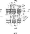
Figure 12 is the schematic elevational view according to sixth embodiment of the invention.
Figure 13 is the cutaway view of being got along Figure 12 center line V3-V3.
Figure 14 is the cutaway view of being got along Figure 12 center line W3-W3.
Figure 15 is the perspective view of the 6th embodiment.
Figure 16 is the schematic cross sectional views according to seventh embodiment of the invention.
Figure 17 is the schematic cross sectional views according to eighth embodiment of the invention.
Figure 18 is the schematic cross sectional views according to ninth embodiment of the invention.
Figure 19 is the schematic cross sectional views according to tenth embodiment of the invention.
Figure 20 is the schematic cross sectional views according to eleventh embodiment of the invention.
Figure 21 is the schematic cross sectional views according to twelveth embodiment of the invention.
Figure 22 is the schematic cross sectional views according to thriteenth embodiment of the invention.
Figure 23 is the schematic cross sectional views according to fourteenth embodiment of the invention.
Figure 24 is the schematic cross sectional views according to fifteenth embodiment of the invention.
Figure 25 is the cutaway view of being got along Figure 24 center line V4-V4.
Figure 26 is the perspective view of the 15 embodiment.
Figure 27 is the schematic elevational view according to sixteenth embodiment of the invention.
Figure 28 is the cutaway view of being got along Figure 27 center line V5-V5.
Figure 29 is the schematic cross sectional views according to seventeenth embodiment of the invention.
Figure 30 is the schematic cross sectional views according to eighteenth embodiment of the invention.
Figure 31 is the perspective view among the 18 embodiment.
Figure 32 is the schematic cross sectional views according to nineteenth embodiment of the invention.
Figure 33 is the perspective view among the 19 embodiment.
Figure 34 is the schematic elevational view of a traditional PD P-structure.
Figure 35 is the cutaway view of being got along Figure 34 center line V-V.
Figure 36 is the cutaway view of being got along Figure 34 center line W-W.
Embodiment
Describe in detail according to a preferred embodiment of the invention hereinafter with reference to accompanying drawing.
Fig. 1 to Fig. 3 is the schematic diagram of first embodiment (hereinafter referred to as " PDP ") according to plasma display panel of the present invention.Fig. 1 is the front view of cellular construction part among first embodiment.Fig. 2 is the cutaway view of being got along Fig. 1 center line V1-V1.Fig. 3 is the perspective view of first embodiment.
PDP shown in Fig. 1 to 3 comprises the front glass substrate 10 as display surface.A plurality of column electrodes are to (X Y) is arranged in the back side of front glass substrate 10, and each column electrode extends the line direction (along the left and right directions among Fig. 1) along substrate 10.
Each column electrode X comprises transparency electrode Xa and black bus electrode Xb, each transparency electrode Xa is formed by the nesa coating of being made by ITO or analog with the T font, and black bus electrode Xb is formed by the wide metal film that the line direction along front glass substrate 10 extends, and is connected to the littler bottom of transparency electrode Xa width.
Similarly, each column electrode Y comprises a transparency electrode Ya and a black bus electrode Yb, each transparency electrode Ya is formed by the nesa coating of being made by ITO or analog with the T font, and black bus electrode Yb is formed by the wide metal film that the line direction along front glass substrate 10 extends, and is connected to the littler bottom of transparency electrode Ya width.
Column electrode X and Y alternately arrange along the column direction (vertical direction among Fig. 1 and the left and right directions among Fig. 2) of front glass substrate 10.Transparency electrode Xa and Ya are spaced routinely along corresponding bus electrode Xb and Yb, and paired transparency electrode Xa and Ya extend in such a way along the right direction of another column electrode, promptly, the bigger front end of each paired transparency electrode Xa and Ya width is provided with the discharging gap g of required width therebetween toward each other.
Each column electrode is to (X Y) forms the display line L that follows the direction extension.
At the back side of front glass substrate 10, form a dielectric layer 11 with cover column electrode to (X, Y).The back side at dielectric layer 11, one additional dielectric layer 12 (among Fig. 2 downwards) from the back side of dielectric layer 11 is backward stretched out, be positioned at the opposite of a presumptive area, as mentioned below, this presumptive area comprises that adjacent each column electrode is to (X, Y) bus electrode Xb and Yb adjacent one another are, and this additional dielectric layer 12 extends in parallel with bus electrode Xb, Yb.
This additional dielectric layer 12 is also as the light absorbing zone that comprises black or dark pigment.
The back side of dielectric layer 11 and additional dielectric layer 12 is coated with the protective layer (not drawing among the figure) that MgO makes.
On the surface of the back glass substrate 13 of display surface one side, a white columns electrode protecting layer (dielectric layer) 14 covers row electrode D, and forms the partition 15 of shape as described below on row electrode protecting layer 14.
If glass substrate 10 is looked in the past, partition 15 is by constituting with the lower part: the first transverse wall 15A, and the edge of the bus electrode Xb of each column electrode X extends by line direction on the side that the bus electrode Yb of the column electrode Y that each first transverse wall 15A edge is paired with it is faced; The edge of the bus electrode Yb of each column electrode Y extends in parallel on the side that the bus electrode Xb of each second transverse wall 15B and paired with it column electrode X is faced, and apart from the first transverse wall 15A one predetermined space is arranged; Each vertical wall 15C extends along a locational column direction between adjacent transparent electrode Xa and the adjacent transparent electrode Ya, and these transparency electrodes Xa and Ya follow electrode X, and respective bus electrode Xb, Yb are spaced with routine among the Y.
Distance between each row electrode protecting layer 14 that is designed to highly equal to cover the protective layer at additional dielectric layer 12 back sides and cover row electrode D of the first transverse wall 15A and vertical wall 15C.The second transverse wall 15B is designed to highly be slightly less than the height of the first transverse wall 15A and vertical wall 15C.That is to say; the front of vertical wall 15C contacts the protective layer back side that covers additional dielectric layer 12 between the front of the first transverse wall 15A (upper surface among Fig. 2) and the first transverse wall 15A and the second transverse wall 15B; and the second transverse wall 15B does not contact the protective layer back side that covers additional dielectric layer 12, and forms a gap r between the protective layer of transverse wall 15B and covering additional dielectric layer 12.
First and second transverse wall 15A of partition 15 and 15B and vertical wall 15C are divided into a plurality of zones to the discharge space between front glass substrate 10 and the back glass substrate 13, each zone is positioned at and is in right and opposite opposed facing transparency electrode Xa and Ya, limits thus to show discharge cell C1.In addition, vertical wall 15C separates the space that forms between the first transverse wall 15A and the second transverse wall 15B, and (X, back-to-back bus electrode Xb Y) and the opposite of Yb are limited to the addressing discharge cell C2 that alternately arranges with demonstration discharge cell C1 on the column direction thus at the adjacent lines electrode pair.
Therebetween have on the column direction with the adjacent demonstration discharge cell C1 of the second transverse wall 15B and addressing discharge cell C2 between link to each other by gap r, gap r is formed between the positive protective layer with covering additional dielectric layer 12 of the second transverse wall 15B.
On the one side of the back glass substrate 13 on each addressing discharge cell C2 opposite, fin 17 stretches out from substrate 13 surfaces on display surface one side, stretch among the addressing discharge cell C2, the height of this fin 17 is lower than the height of the second transverse wall 15B, and extends by band shape on line direction.
Like this; the part of the row electrode D on each addressing discharge cell C2 opposite is raised from back glass substrate 13 by fin 17 with the row electrode protecting layer 14 of this part that covers row electrode D; to stretch among each addressing discharge cell C2; this part of the row electrode D on addressing discharge cell C2 opposite and the space interval s2 between bus electrode Xb and the Yb are less than a part and the transparency electrode Xa of the row electrode D that shows discharge cell C1 opposite, the space interval s1 between the Ya thus.
Be filled with discharge gas among each demonstration discharge cell C1 and each addressing discharge cell C2.
A kind of like this PDP produces image by following process.
At first, show among the discharge cell C1, in the reset cycle, cause reset discharge, on the surface of dielectric layer 11, to form the wall electric charge at each.
In the addressing period after the reset cycle, the one scan pulse is applied on the column electrode Y, and data pulse is applied on the row electrode D.
So the column electrode Y that is applied with scanning impulse between electrode Y and D begins address discharge with the place, row electrode D crosspoint that is applied with data pulse.In this, address discharge mainly results between the bus electrode Yb that fin 17 stretches into the part of the row electrode D among the addressing discharge cell C2 and column electrode Y, because the space interval s2 between the bus electrode Yb of column electrode Y respect to one another and the row electrode D is less than transparency electrode Ya that shows column electrode Y respect to one another among the discharge cell C1 and the space interval s1 between the row electrode D among the addressing discharge cell C2.
The charged particle that address discharge among the addressing discharge cell C2 produces passes the gap r that forms between the second transverse wall 15B and the additional dielectric layer 12, among the demonstration discharge cell C1 of inflow and addressing discharge cell C2 adjacency, thereby eliminate the wall electric charge that forms in the face of on the dielectric layer 11 that shows discharge cell C1, the second transverse wall 15B is arranged between discharge cell C1 and the C2.Like this, luminescence unit (at the demonstration discharge cell C1 that forms the wall electric charge on the dielectric layer 11) and not luminescence unit (not forming the demonstration discharge cell C1 of wall electric charge on the dielectric layer 11) according to image distribution to display in lip-deep all the display line L of plate.
In the lasting light period after finishing addressing period, simultaneously a discharge sustain pulse alternately is applied among each display line L each column electrode to (X, Y) on.Apply this discharge sustain pulse each time, just begin continuous discharge between relative transparency electrode Xa in each luminescence unit and the Ya, produce ultraviolet ray thus.What produced is ultraviolet ray excited in the face of each red (R) that shows discharge cell C1, green (G) and blue (B) fluorescence coating 16.
For above PDP, in each discharge cell, respectively independently produce address discharge and continuous discharge, address discharge is used for according to image to display luminescence unit and luminescence unit not being distributed on the plate surface, and continuous discharge is used for making fluorescence coating 16 to send colourama.Two purposes can be successfully finished simultaneously in this design: reduce the starting voltage of address discharge, this be because fin 17 in addressing discharge cell C2 row electrode D and the bus electrode Yb of column electrode Y between a littler space interval s2 is provided; Improve luminous efficiency, design greatlyyer (that is,, a bigger space interval s1 being arranged between Ya and the row electrode D) at transparency electrode Xa because will show the discharge space among the discharge cell C1.
In addition, in this PDP, in having the addressing discharge cell C2 of fluorescence coating, do not produce address discharge, so that a stable address discharge is provided, and do not resemble wherein the influence that is subjected to following situation the traditional PD P that causes address discharge between two electrodes of a fluorescence coating being inserted with: with forming fluorescence coating and having the discharge performance that versicolor fluorescent material changes, the varied in thickness of fluorescence coating etc.
During space interval s2 in determining addressing discharge cell C2 between row electrode D and the bus electrode Yb, preferably referring to the scope in the Paschen figure shown in Fig. 4, in this scope, address discharge starting voltage by the line v1 indication of representing the address discharge starting voltage is very low, and show forward characteristic (increasing the characteristic of discharge voltage value with the increase of pressure in the discharge space), this scope is around the line v1 minimum point and the zone (zone of " E " indication among Fig. 4) on minimum point right side.
In this way, as definite space interval s2 so that the address discharge starting voltage when falling into the area E of line v1, can reduce the starting voltage of address discharge among the PDP.In addition, because the little variation of the discharge voltage that pressure causes in the area E allows the height change (being that space interval s2 changes) of fin 17, make its minimum that influences to address discharge voltage.
Should be pointed out that in first embodiment, space interval s2 is defined as 70 microns.
In above PDP, the charged particle that address discharge produced among addressing discharge cell C2 passes the gap r that forms between the additional dielectric layer 12 and the second transverse wall 15B, flow into and show discharge cell C1, in showing discharge cell C1, the bus electrode Yb of transparency electrode Ya from be included in the beginning address discharge extends.This aspect on, additional dielectric layer 12 contact first transverse wall 15A and vertical wall 15C, so that relevant addressing discharge cell C2 forms obstruct with it between adjacent on the opposite column direction but unconnected demonstration discharge cell C1, and make relevant addressing discharge cell C2 and its between addressing discharge cell C2 adjacent on the both sides of line direction, form obstruct.Like this, prevented that charged particle from flowing among such demonstration discharge cell C1 who does not connect and the addressing discharge cell C2 adjacent with relevant addressing discharge cell C2.
By additional dielectric layer 12, prevented from also to show that the charged particle that continuous discharge produced among the discharge cell C1 flows among the addressing discharge cell C2 that does not connect that is adjacent.
In addition, additional dielectric layer 12 as the light absorbing zone that comprises black or dark pigment has prevented that the light that address discharge produced among the addressing discharge cell C2 from leaking the display surface of glass substrate 10 forward, and the reflection of ambient light that prevents to pass front glass substrate 10 to the corresponding zone of addressing discharge cell C2 on, improved the contrast of display image thus.
In order to make one to show discharge cell C1 and be communicated with between the addressing discharge cell C2 accordingly, in aforementioned content, be defined as being lower than the height of the first transverse wall 15A by height, in the additional dielectric layer 12 and the second transverse wall 15A, form gap r the second transverse wall 15B.On the other hand, can show the groove that is communicated with between discharge cell C1 and the respective addressed discharge cell C2 being formed on one on the top of the second transverse wall 15B highly identical with the first transverse wall 15A.As another conversion, can with additional dielectric layer that second transverse wall contacts on form and show the groove that is communicated with between discharge cell C1 and the respective addressed discharge cell C2, the height of second transverse wall is identical with the height of the first transverse wall 15A.As another conversion, can alternately place second transverse wall highly identical since an additional dielectric layer, to be formed on the communication gap that shows between discharge cell C1 and the corresponding addressing discharge cell C2 with the first transverse wall 15A.
Fig. 5 and 6 is the schematic diagrames according to PDP second embodiment of the present invention.Fig. 5 is the front view of PDP cellular construction part among second embodiment.Fig. 6 is the cutaway view along V2-V2 line among Fig. 5.
In the PDP of second embodiment, the bus electrode X1b of a column electrode X1 is placed the position on the first transverse wall 15A opposite.The transparency electrode X1a bottom X1a ' that is connected to bus electrode X1b extends to the position on the row electrode D part opposite that is positioned on the fin 17, and addressing discharge cell C2 inserts wherein.
Similarly, the bus electrode Y1b of column electrode Y1 is placed the position on the second transverse wall 15B opposite.The bottom Y1a ' that is connected to the transparency electrode Y1a of bus electrode Y1b extends to the position on the row electrode D part opposite that is positioned on the fin 17, and addressing discharge cell C2 inserts wherein.
Among second embodiment among the structure of miscellaneous part and first embodiment modular construction of PDP therefore adopt identical reference number much at one.
First embodiment has described the address discharge that produces between the bus electrode Yb and fin 17 above-listed electrode D among the addressing discharge cell C2, and second embodiment has described such PDP, wherein at the row electrode D on the fin 17 and extend to from bus electrode between the transparency electrode Ya bottom Y1a ' of position, addressing discharge cell C2 opposite and cause address discharge.
Fig. 7 is the PDP cutaway view by third embodiment of the invention, be with Fig. 2 in the cutaway view got of identical position.
PDP among the 3rd embodiment have with first embodiment in the similar structure of PDP, each column electrode X wherein, each bus electrode Xb of Y, Yb is positioned at addressing discharge cell C2 opposite, and a black conductive layer is arranged.Be seated among the adjacent display line L back-to-back, and between the bus electrode Xb and Yb on same addressing discharge cell C2 opposite, black or dark light absorbing zone 20 extend on line direction.The light absorbing zone 20 of bus electrode Xb and Yb and black or dark conductive layer coverage rate are to the one side of the addressing discharge cell C2 of front glass substrate 10.
Among the 3rd embodiment among the structure of miscellaneous part and first embodiment modular construction of PDP therefore adopt identical reference number indication much at one.
For the PDP according to the 3rd embodiment, the light that produces among the addressing discharge cell C2 is subjected to the light absorbing zone 20 of bus electrode Xb and Yb light and black or dark conductive layer to be stopped, and is prevented from leak the display surface of glass substrate 10 forward.And, the reflection of ambient light that prevents to pass front glass substrate 10 to the corresponding zone of addressing discharge cell C2 on.Therefore, improved the contrast in the display image.
Fig. 8 and Fig. 9 are the schematic diagrames that illustrates according to PDP the 4th embodiment of the present invention.Fig. 8 is the cutaway view of PDP among the 4th embodiment, be along with Fig. 2 in the cutaway view got of identical position.Fig. 9 is the perspective view of the 4th embodiment.
PDP among the 4th embodiment have with first embodiment in the similar structure of PDP; but be not on the part on row electrode opposite at row electrode protecting layer 14, the first transverse wall 15A, the second transverse wall 15B and vertical wall 15C, discharge be set in each addressing discharge cell C2 start particle generation layer 30.
This discharge starts particle and produces layer 30 and formed by the ultra-violet (UV) band luminescent material with sunset glow characteristic, wherein, for example this material is subjected to predetermined wavelength or long wavelength ultraviolet ray excited more, ultraviolet with continuous emission for up to 0.1 millisecond or longer time, the addressing period of reaching length or longer time (for example 1.0 milliseconds or longer time) are preferably arranged.
This discharge that is formed by the ultra-violet (UV) band luminescent material starts particle generation layer 30 can comprise the material that has than low work function (for example 4.2eV or littler),, has the material (high γ (gamma) material) of higher secondary electron yield that is.
Examples of materials with little work function and insulation characterisitic comprises: alkali metal oxide (Cs for example
2O: work function 2.3eV); Alkaline earth oxide (for example CaO, SrO, BaO); Fluoride (CaF for example
2, MgF
2); In crystal, produce lattice defect, impurity or analog and think that the coefficient of secondary increases discharge and the material (for example, have the Mg that changed from 1: 1: the O proportioning is to produce the MgOx of crystal defect) of generation imperfection energy level; TiO
2Y
2O
3Or the like.
Another kind of ultra-violet (UV) band luminescent material has the sunset glow characteristic, wherein, during the vacuum ultraviolet (VUV) optical excitation of 147 nano wave lengths that in these materials are subjected to by the xenon that comprises from discharge gas of discharge, send, 1.0 milliseconds or the ultraviolet ray of (being the duration or the longer time of addressing period) are for more time preferably launched in 0.1 millisecond of emission or the ultraviolet ray of longer time continuously.The example of this ultra-violet (UV) band luminescent material comprises BaSi
2O
5: Pb
2+(the issued light wavelength: 350 nanometers), SrB
4O
7F:Eu
2+(the issued light wavelength: 360 nanometers), (Ba, Mg, Zn)
3Si
2O
7: Pb
2+(the issued light wavelength: 295 nanometers), YF
3: Gd, Pr, or the like.
Among the 4th embodiment among the structure of miscellaneous part and first embodiment structure of PDP therefore adopt identical reference number indication much at one.
In the PDP of the 4th embodiment, reset discharge by reset cycle while, send the vacuum-ultraviolet light of 147 nano wave lengths in the xenon that from discharge gas, comprises, wherein in all demonstration discharge cell C1, form (or cancellation) wall electric charge, then, excite the discharge that is arranged among each addressing discharge cell C2 to start particle and produce layer 30, so that it sends ultraviolet light.This ultraviolet excitation covers the protective layer (MgO layer) of additional dielectric layer 12, and if its discharge of comprising high γ material start particle and produce layer 30, then allow their emission discharges to start particle.
Discharge starts particle generation layer 30 a continuous emission ultraviolet light and reaches at least 0.1 millisecond or longer time, because the sunset glow characteristic of the ultra-violet (UV) band luminescent material of formation this layer 30 is arranged.Like this, during the addressing period after the reset cycle, can guarantee in each addressing discharge cell C2, to have the discharge startup particle of q.s to cause address discharge at the same time.Therefore, after finishing reset discharge, what prevent that guiding discharge from starting that grain amount reduces in time in the past misplaces electricity or the generation of the incident that lags behind discharge time.
Figure 10 and Figure 11 are the schematic diagrames according to PDP the 5th embodiment of the present invention.Figure 10 is the cutaway view along PDP among the 5th embodiment that is got with Fig. 2 same position.Figure 11 is the perspective view among the 5th embodiment.
The PDP part that PDP among the 5th embodiment is different among first to fourth embodiment is, in order to make row electrode close bus electrode in each addressing discharge cell, fin is not set, therefore even in the zone relative, also row electrode D1 is made rectilinear form with addressing discharge cell C2 '.
In addressing discharge cell C2 ', setting has 50 or the dielectric layer 40 that forms of the high ε material of the relative dielectric constant of higher (50 to 250), so that dwindle the discharge space (space interval between bus electrode Yb and the dielectric layer 40) among each addressing discharge cell C2 '.
Dielectric layer 40 examples of high ε material are SrTiO
3
Among the 5th embodiment among the structure of miscellaneous part and first embodiment structure of PDP much at one, so adopt the indication of identical reference number.
Among the PDP in the 5th embodiment, produce address discharge between electrode D in addressing discharge cell C2 ' and the Yb, be inserted with the high ε material that forms dielectric layer 40 between two electrodes, this high ε material has 50 or higher relative dielectric constant (ε).Therefore, shorten the row electrode D1 and the interval of the surface discharge between the bus electrode Yb that cause address discharge, caused reducing the starting voltage of address discharge.
Figure 12 to Figure 15 is the schematic diagram according to sixth embodiment of the invention.Figure 12 is the front view of the discharge cell structure division of PDP among the 6th embodiment.Figure 13 is the cutaway view of being got along V3-V3 line among Figure 12.Figure 14 is the cutaway view of being got along W3-W3 line among Figure 12.Figure 15 is the perspective view of the 6th embodiment.
PDP basic structure configuration shown in Figure 12 to Figure 15 is roughly the same with the structure of the middle PDP of first embodiment (Fig. 1 to 3), with those the same or analogous parts of PDP among the same or analogous reference number indication and first embodiment.
Among the PDP addressing discharge cell C2 in the 6th embodiment, a pair of vertical ribs 50 is extended along column direction between the first transverse wall 15A on the row electrode D both sides and the second transverse wall 15B.This to vertical ribs 50 also with in the addressing discharge cell C2 without separating into the first addressing discharge cell C2a and the second addressing discharge cell C2b, the first addressing discharge cell C2a is positioned at the middle body of addressing discharge cell C2 and on row electrode D opposite, the second addressing discharge cell C2b is positioned at the first addressing discharge cell C2a both sides.
Be provided with a dielectric layer 51 among each first addressing discharge cell C2a, this dielectric layer 51 is formed by the material with high relative dielectric constant (for example ε=50 are to 250), as SrTiO
3(hereinafter referred to as " high ε material ").Dielectric layer 51 has dwindled the discharge space (space interval between bus electrode Yb and the dielectric layer 51) among each first addressing discharge cell C2a.
Do not form anything in each the second addressing discharge cell C2b inside that is positioned at the first addressing discharge cell C2a both sides, that is, the second addressing discharge cell C2b is a hollow.
Be filled with discharge gas among each demonstration discharge cell C1 and the addressing discharge cell C2.
It is as follows to generate image on PDP.
At first, by the reset discharge in the reset cycle, form the wall electric charge on the surface of the dielectric layer 11 in each demonstration discharge cell C1.
In the addressing period after the reset cycle, scanning impulse is applied on the column electrode Y, and data pulse is applied on the row electrode D.
In this, because the high ε material that forms dielectric layer 51 is arranged in the first addressing discharge cell C2a of addressing discharge cell C2, so the virtual discharge interval s3 between row electrode D and the bus electrode Yb is less than the interval s4 between row electrode D and the transparency electrode Ya, row electrode D is relative with transparency electrode Ya, and the discharge cell of demonstration C1 is arranged therebetween.Therefore, cause address discharge between row electrode D and bus electrode Yb, row electrode D is relative with bus electrode Yb, and the first addressing discharge cell C2a is arranged therebetween.
The charged particle that produces by address discharge among the first addressing discharge cell C2a passes the gap r between the second transverse wall 15B and the first additional dielectric layer 12A, flow among the demonstration discharge cell C1 of the unit C2a adjacency relevant then, face the wall electric charge that forms on dielectric layer 11 parts of discharge cell C1 thereby eliminate with the second transverse wall 15B therebetween.Like this, luminescence unit (wherein at the demonstration discharge cell C1 that forms the wall electric charge on the dielectric layer 11) and not luminescence unit (wherein not forming the demonstration discharge cell C1 of wall electric charge on the dielectric layer 11) according to image distribution to display on the plate surface.
This aspect on, it is adjacent but among unconnected demonstration discharge cell C1 that the charged particle that produces by the address discharge on the addressing discharge cell C2 does not flow into the unit C2 relevant with the first transverse wall 15A therebetween, because be provided with the second additional dielectric layer 12B, so that relevant unit C2 and unconnected unit C1 obstruct are opened.
In the lasting light period after finishing addressing period, simultaneously the discharge sustain pulse alternately is applied among each display line L column electrode to (X, Y) on.Apply this discharge sustain pulse each time, just in each luminescence unit, begin continuous discharge between relative transparency electrode Xa and the Ya, produce ultraviolet ray thus.What produced is ultraviolet ray excited in the face of red (R) that shows discharge cell C1, green (G) and blue (B) fluorescence coating 16, thereby forms display image.
For above PDP, in being independent of the addressing discharge cell C2 that shows discharge cell C1, produce address discharge, and in showing discharge cell C1, produce continuous discharge.Along with being arranged, the high ε material insertion that forms dielectric layer 51 produces address discharge between electrode Yb and the D in the first addressing discharge cell C2a, therefore shortened the surface discharge interval between row electrode D and the bus electrode Yb, thereby compared with the prior art, significantly reduced the starting voltage of address discharge.
In addition, in this PDP, by vertical ribs 50 addressing discharge cell C2 is divided into the first addressing discharge cell C2a and the second addressing discharge cell C2b, 51 of dielectric layers are formed at the first addressing discharge cell C2a that is arranged in addressing discharge cell C2 middle body row electrode D opposite, wherein, do not form address discharge and begin unwanted dielectric layer.This design does not allow PDP between adjacent column electrode D disadvantageous interelectrode capacitance to be arranged, and has prevented unnecessary electrical power consumed thus.
In addition, in this PDP, in being independent of the addressing discharge cell C2 that shows discharge cell C1, produce address discharge, and in showing discharge cell C1, produce continuous discharge.For this reason, can improve luminous efficiency by limit a bigger discharge space (at transparency electrode Xa, than long interval s4 between Ya and the row electrode D) in showing discharge cell C1, this does not influence the discharge inception voltage of address discharge.
Figure 16 is the cutaway view of the 7th embodiment of one PDP according to the present invention, is the cutaway view of getting along the position identical with the 6th embodiment Figure 14.
Among the PDP in the 7th embodiment, a discharge is set in each second addressing discharge cell C2b starts particle and produce layer 52, in the 6th embodiment, the second addressing discharge cell C2b is designed to hollow.
This discharge starts particle and produces layer 52 and made by the ultra-violet (UV) band luminescent material with sunset glow characteristic, wherein, for example, with having predetermined wavelength or ultraviolet ray excited this material of long wavelength more, reach 0.1 millisecond or longer time with continuous emission ultraviolet ray, preferably reach the duration or the longer time (for example 1.0 milliseconds or longer time) of addressing period.
The discharge that the ultra-violet (UV) band luminescent material is made starts particle generation layer 52 can comprise the material that has than low work function (for example 4.2eV or littler),, has the material (high γ material) of higher secondary electron yield that is.
Examples of materials with little work function and insulation characterisitic comprises: alkali metal oxide (Cs for example
2O: work function 2.3eV); Alkaline earth oxide (for example CaO, SrO, BaO); Fluoride (CaF for example
2, MgF
2); In crystal, produce lattice defect, impurity or analog, the material of imperfection energy level (for example, have the Mg that changed from 1: 1: the O proportioning is to produce the MgOx of crystal defect) is arranged for making secondary electron yield increase discharge generation; TiO
2Y
2O
3Or the like.
Another kind of ultra-violet (UV) band luminescent material has the sunset glow characteristic, during the 147 nano wave length vacuum ultraviolet (VUV) optical excitation of wherein in these materials are subjected to by the xenon that comprises from discharge gas of discharge, sending, 1.0 milliseconds or the ultraviolet ray of (being the duration or the longer time of addressing period) are for more time preferably launched in 0.1 millisecond of emission or the ultraviolet ray of longer time continuously.The example of this ultra-violet (UV) band luminescent material comprises BaSi
2O
5: Pb
2+(the issued light wavelength: 350 nanometers), SrB
4O
7F:Eu
2+(the issued light wavelength: 360 nanometers), (Ba, Mg, Zn)
3Si
2O
7: Pb
2+(the issued light wavelength: 295 nanometers), YF
3: Gd, Pr, or the like.
Among the 7th embodiment among the structure of miscellaneous part and the 6th embodiment structure of PDP therefore adopt identical reference number indication much at one.
In the PDP of the 7th embodiment, reset discharge by reset cycle while, send the vacuum-ultraviolet light of 147 nano wave lengths in the xenon that from discharge gas, comprises, wherein in all demonstration discharge cell C1, form (or cancellation) wall electric charge, excite the discharge that is arranged among each second addressing discharge cell C2b to start particle then and produce layer 52, make it send ultraviolet light.This ultraviolet excitation covers the protective layer (MgO layer) of the first and second additional dielectric layer 12A and 12B; if and discharge starts particle and produce layer 52 and comprise the ultraviolet excitation cover layer, the discharge of so high γ material starts particle and produces layer 52 and can allow their emission discharges to start particle.
Discharge starts particle generation layer 52 a continuous emission ultraviolet light and reaches at least 0.1 millisecond or longer time, because the sunset glow characteristic of the ultra-violet (UV) band luminescent material of formation this layer 52 is arranged.Like this, at the same time during the addressing period after the reset cycle, can guarantee in each addressing discharge cell C2, to have the discharge startup particle of q.s to cause address discharge, therefore, after finishing reset discharge, what prevent that guiding discharge from starting that grain amount reduces to take place in time in the past misplaces electricity or the incident that lags behind discharge time.
Figure 17 is the cutaway view of the 8th embodiment of PDP according to the present invention, and it is the cutaway view of getting along the position identical with the 6th embodiment.
PDP among the 6th embodiment has another kind of structure, that is, column electrode X and Y along column direction with X-Y, X-Y ... mode arrange; And the PDP among the 8th embodiment has a kind of like this structure, wherein in each display line, and adjacent lines electrode pair on the column direction (X, Y) column electrode X and Y change on the position, that is, two of same type electrodes with X-Y, Y-X, X-Y ... the back-to-back arrangement of mode.
In the PDP of the 8th embodiment, addressing discharge cell C2 ' is arranged on adjacent lines electrode pair (X, Y) the double bus electrode Yb opposite of back-to-back column electrode Y, and be common to and be positioned on the column direction two on the addressing discharge cell C2 ' both sides and show between the discharge cell C1.51 of dielectric layers are formed among the first addressing discharge cell C2a in the face of each column electrode Y bus electrode Yb.
(X, Y) between the double bus electrode Yb of back-to-back column electrode Y on the position on regional opposite, the second additional dielectric layer 12B ' follows direction (perpendicular to the direction of Figure 17) and extends on the back side of the first additional dielectric layer 12A at the adjacent lines electrode pair.The second additional dielectric layer 12B ' has the back side of contact dielectric layer 51, and the space between the first additional dielectric layer 12A and the dielectric layer 51 is divided into two, to form the separation addressing discharge cell C2a ' of a pair of back-to-back storing.
One on the left side of separating among the addressing discharge cell C2a ' is connected to the demonstration discharge cell C1 that is adjacent by gap r, between these two discharge cells the second transverse wall 15B is arranged, and this gap r is formed between the first additional dielectric layer 12A and the second transverse wall 15B.
One on the right of separating among the addressing discharge cell C2a ' is connected to a demonstration discharge cell C1 who is adjacent by a gap r ', between these two discharge cells the second transverse wall 15A is arranged, and this gap r ' is formed between the first additional dielectric layer 12A and the first transverse wall 15A.
The unit C on the bus electrode Xb opposite of each column electrode X of back-to-back arrangement " be hollow.The 3rd additional dielectric layer 12C is formed at the almost whole back side of the first additional dielectric layer 12A, and contact is positioned at unit C2 " the first and second transverse wall 15A and the 15B front end face of both sides; in order at unit C2 " and the demonstration discharge cell C1 that is adjacent between form and intercept, the first transverse wall 15A and the second transverse wall 15B are between these two unit.
Among the 8th embodiment among the structure of miscellaneous part and the 6th embodiment structure of PDP therefore adopt identical reference number indication much at one.
Among the PDP in the 8th embodiment, produce address discharge between bus electrode Yb in the first addressing discharge cell C2a ' and the row electrode D, the first addressing discharge cell C2a ' by the second additional dielectric layer 12B ' separately and between the first additional dielectric layer 12A and dielectric layer 51.The charged particle that produces by address discharge passes the gap r between the first additional dielectric layer 12A and the second transverse wall 15B, and first the gap r ' between additional dielectric layer 12A and the first transverse wall 15A, flow among the corresponding demonstration discharge cell C1 adjacent with the addressing discharge cell C2a ' that respectively separates.
In this way, the PDP among the 8th embodiment has the column electrode X of back-to-back setting on column direction and the column electrode Y of back-to-back setting.For this structure, when the discharge sustain pulse being applied to column electrode to (X when Y) going up with the beginning continuous discharge, does not form discharge capacity in the non-display area on line direction between the column electrode of back-to-back setting, prevent to exist reactive power thus.
Figure 18 is the cutaway view of the 9th embodiment of PDP according to the present invention, and it is the cutaway view of getting along the position identical with position among the 6th embodiment Figure 13.
Substituting PDP among dielectric layer 51, the nine embodiment that high ε material is made among the 6th embodiment has the conductive layer 61 that is formed by conductive material such as silver or analog, and this conductive layer 61 is arranged among each addressing discharge cell C2a of addressing discharge cell.
Among the 9th embodiment among the structure of miscellaneous part and the 6th embodiment structure of PDP therefore adopt identical reference number indication much at one.
In the PDP of the 9th embodiment, also in addressing discharge cell, produce address discharge, addressing discharge cell separates with the demonstration discharge cell C1 that is used for continuous discharge, is inserted in the conductive material that forms conductive layer 61 among the first addressing discharge cell C2a of addressing discharge cell between Unit two.Therefore, shortened the discharge interval between row electrode D and the bus electrode Yb, compared, significantly reduced the starting voltage of address discharge with the voltage in the prior art.
Figure 19 is the cutaway view of the tenth embodiment of PDP according to the present invention, and it is the cutaway view of getting along the position identical with position among the 6th embodiment Figure 13.
PDP among the tenth embodiment comprises what high ε material formed, and, be arranged on conductive layer 61 lip-deep dielectric layers 62, it is on the opposite of the first additional dielectric layer 12A, conductive layer 61 is made by conductive material such as silver or analog, and, be arranged among each addressing discharge cell C2a of addressing discharge cell.
Among the tenth embodiment among the structure of miscellaneous part and the 6th embodiment structure of PDP therefore adopt identical reference number indication much at one.
As under the situation of the 6th embodiment, in the PDP of the tenth embodiment, with be used for the demonstration discharge cell C1 of continuous discharge and separate in the addressing discharge cell that forms, between electrode Yd and D, produce address discharge, insert high ε material that forms dielectric layer 62 and the conductive material that forms conductive layer 61 between Unit two.Therefore, by conductive layer 61 shortened between row electrode D and the bus electrode Yb discharge at interval, and by dielectric layer 62 shortened greatly between row electrode D and the bus electrode Yb surface discharge at interval, thereby compare with the voltage in the prior art, significantly reduced the starting voltage of address discharge.
Figure 20 is the cutaway view according to PDP the 11 embodiment of the present invention, and it is the cutaway view of getting along the position identical with the 6th embodiment Figure 13 position.
As under the situation of PDP among the 8th embodiment, PDP among the 11 embodiment has a kind of like this structure, in this structure, adjacent lines electrode pair (X on the column direction, Y) column electrode X and Y are equipped with institute's conversion in that each bar display line is upper, with X-Y, Y-X, X-Y ... mode make the back-to-back setting of two electrodes of same type.
As under the situation of PDP among the tenth embodiment, the dielectric layer 62 that conductive layer 61 that electric conducting material is made and high ε material are made is arranged among each first addressing discharge cell C2a of addressing discharge cell C2 '.
Among the 11 embodiment among the structure of miscellaneous part and the 8th embodiment structure of PDP therefore adopt identical reference number indication much at one.
As under the situation of PDP among the 8th embodiment, PDP has the structure of the back-to-back setting of column electrode X and the back-to-back setting of column electrode Y on column direction among the 11 embodiment.When the discharge sustain pulse being applied to column electrode to (X, when Y) going up with the beginning continuous discharge, this structure makes does not have discharge capacity in the non-display area between the column electrode of PDP back-to-back setting on column direction, has prevented reactive power thus.In addition, as under the situation of PDP among the tenth embodiment, at the addressing discharge cell C2 ' that separates with the demonstration discharge cell C2 that is used for continuous discharge, between electrode Yb and D, produce address discharge, insert high ε material that forms dielectric layer 62 and the electric conducting material that forms conductive layer 61 between Unit two.Therefore, by the discharge between conductive layer 61 shortening row electrode D and the bus electrode Yb at interval, and by dielectric layer 62 shortened greatly again between row electrode D and the bus electrode Yb surface discharge at interval, thereby compared with the prior art, significantly reduced the starting voltage of address discharge.
Figure 21 is the cutaway view of the 12 embodiment of PDP according to the present invention, and it is the cutaway view of getting along the position identical with the 6th embodiment Figure 13 position.
The PDP of the 9th embodiment so constitutes, that is, conductive layer 61 is electrically connected on the row electrode D, inserts row electrode protecting layer 14 between the two.In the PDP of the 12 embodiment, as shown in figure 21, conductive layer 61 and row electrode D are electrically connected by a through hole 63, and this through hole 63 is arranged in the row electrode protecting layer 14 '.
Therefore structure among the 12 embodiment among the PDP of the structure of miscellaneous part and the 9th embodiment adopts identical reference number indication much at one.
PDP for the 12 embodiment; be electrically connected owing to exist between the conductive layer 61 that is inserted with row electrode protecting layer 14 ' between the two and the row electrode D; so further shortened the discharge interval between row electrode D and each the bus electrode Yb; thereby compared with the prior art, significantly reduced the starting voltage of address discharge.
Figure 22 is the cutaway view of PDP the 13 embodiment according to the present invention, and it is the cutaway view of getting along the position identical with position among the 6th embodiment Figure 13.
Therefore structure among the 13 embodiment among the PDP of the structure of miscellaneous part and the tenth embodiment adopts identical reference number indication much at one.
PDP for the 13 embodiment; be electrically connected owing to exist between the conductive layer 61 that is inserted with row electrode protecting layer 14 ' between the two and the row electrode D; so further shortened the discharge interval between row electrode D and each the bus electrode Yb; thereby compared with the prior art, significantly reduced the starting voltage of address discharge.
Figure 23 is the cutaway view of PDP the 14 embodiment according to the present invention, and it is the cutaway view of getting along the position identical with position among the 6th embodiment Figure 13.
The PDP of the 14 embodiment also comprises these electrodes Yb1 shared between the column electrode Y of bus electrode Xb1 shared between the column electrode X of back-to-back setting and back-to-back setting.
Therefore structure among the 14 embodiment among the PDP of the structure of miscellaneous part and the 11 embodiment adopts identical reference number indication much at one.
PDP for the 14 embodiment; be electrically connected owing to exist between the conductive layer 61 that is inserted with row electrode protecting layer 14 ' between the two and the row electrode D; so further shortened the discharge interval between row electrode D and each the bus electrode Yb; thereby compared with the prior art, significantly reduced the starting voltage of address discharge.
Among each embodiment in the 6th to the 14 embodiment, the first additional dielectric layer 12A is as black or dark light absorbing zone, to prevent leaking display surface to display panel by the light that address discharge was produced among each addressing discharge cell C2.Perhaps, the first additional dielectric layer 12A is not used as light absorbing zone, but with each bus electrode Xb, Yb is designed to comprise the sandwich construction of a black layer, and black or dark light absorbing zone can be set between back-to-back bus electrode, to prevent leaking display surface to display panel by address discharge was produced among each addressing discharge cell C2 light.
Figure 24 to Figure 26 is the schematic diagram of PDP the 15 embodiment according to the present invention.Figure 24 is the front view of PDP cellular construction part among the 15 embodiment.Figure 25 is the cutaway view along V4-V4 line among Figure 24.Figure 26 is the perspective view that the 15 embodiment is shown.
Structure among Figure 24 to Figure 26 among the basic structure of PDP and first embodiment (Fig. 1 to 3) refers to identical reference number with same or analogous each parts of those parts among first embodiment much at one.
Each column electrode X2 of PDP is by constituting with the lower part among the 15 embodiment: transparency electrode X2a, the T font nesa coating of being made up of big width front end Xa1 and less width bottom Xa2 that each transparency electrode X2a makes with ITO or analog forms, and the parallel column direction extension of edge and front glass substrate 10; One black bus electrode X2b, it is formed by a metal film, extends along the line direction of front glass substrate 10, and is connected to the bottom of each less width of transparency electrode X2a.
Similarly, each column electrode Y2 of PDP is by constituting with the lower part: transparency electrode Y2a, their each T font nesa coating of being made up of big width front end Ya1 and less width bottom Ya2 made from ITO or analog forms, and the parallel column direction extension of edge and front glass substrate 10; One black bus electrode Y2b, it is formed by a metal film, extends along the line direction of front glass substrate 10, and is connected to the bottom of each less width of transparency electrode Y2a.
Column electrode X2 and Y2 are arranged alternately on the column direction (vertical direction among Figure 24, the left and right directions among Figure 25) of front glass substrate 10.Transparency electrode X2a and Y2a are provided with routinely at interval along corresponding bus electrode X2b and Y2b.Transparency electrode X2a extends along the direction of the transparency electrode Y2a of its pairing, and vice versa, so that the front end Xa1 of each transparency electrode X2a and Y2a and Ya1 face and have between the two the discharging gap g of Rack mutually.
Column electrode X2, each the transparency electrode X2a of Y2 and the front end Xa1 of Y2a and Ya1 on the direction of front glass substrate 10 with respect to each the bottom Xa2 and the Ya2 bending that extend in parallel with front glass substrate 10, thereby as seen in Figure 25, the front end face that stretches out continuously from the back side of each bottom Xa2, Ya2 almost is parallel to each other and faces.
In the locational dielectric layer 11 ' a groove 11a is set between transparency electrode X2b and opposed facing front end Xa1 of Y2b and Ya1, this groove 11a is inserted between the front end Xa1 and Ya1 of transparency electrode X2a and Y2a as the vacuum space.
As under the situation among the first embodiment PDP, produce image among the PDP of the 15 embodiment.Produce the column electrode X2 of continuous discharge therebetween, the transparency electrode X2a of Y2, Y2a and not according to the tradition design setting, in the tradition design, the front end of electrode join end to end mutually (seeing Figure 35).Transparency electrode X2a, the front end Xa1 of Y2a, Ya1 are with respect to bottom Xa2, and Ya2 is crooked respectively, almost faces mutually abreast.In dielectric layer 11 ', groove 11a is formed at transparency electrode X2a, and Y2a is mutually in the face of a position between front end Xa1 and the Ya1.Groove 11a has the function of a vacuum space, in order to when continuous discharge takes place, shortens the interval of the electric wire power of passing dielectric layer 11 ' inside, thus compared with the prior art, has increased the electric field strength of electric wire power.
Therefore, even when improving luminous efficiency and make discharge gas that high xenon content be arranged, this PDP also can start continuous discharge under low driving voltage.
In PDP, groove 11a can independently be formed at each and show among the discharge cell C1, perhaps is formed in the band shape of line direction extension.
This groove can directly be formed on the back side of front glass substrate 10, and this groove is used for making column electrode to (X1, Y1) each transparency electrode Xa and Ya face mutually, and provide the vacuum space between transparency electrode X2a and Y2a.
Figure 27 and Figure 28 are the schematic diagrames of PDP the 16 embodiment according to the present invention.Figure 27 is the part front view of PDP cellular construction among the 16 embodiment.Figure 28 is the cutaway view along V5-V5 line among Figure 27.
PDP among the 16 embodiment so constitutes, promptly, the bus electrode X3b of column electrode X3 is positioned at the opposite of the first transverse wall 15A, and the bottom X3a ' of transparency electrode X3a is connected to bus electrode X3b, and extend to a position on the row electrode D opposite that places on the fin 17, addressing discharge cell C2 is arranged therebetween.
Similarly, the bus electrode Y3b of column electrode Y3 is positioned at the opposite of the second transverse wall 15B, and the bottom Y3a ' of transparency electrode Y3a is connected to bus electrode Y3b, and extends to a position on the row electrode D opposite that places on the fin 17, and addressing discharge cell C2 is arranged therebetween.
Among the 16 embodiment among the structure of miscellaneous part and the 15 embodiment structure of PDP much at one, it adopts the indication of identical reference number.
PDP among the 15 embodiment constitutes and makes among each addressing discharge cell C2, produces address discharge placing between bus electrode Y2b on the fin 17 and the row electrode D; And the PDP among the 16 embodiment is constructed such that placing the row electrode D on the fin 17 and extend to from bus electrode Y3b between the bottom Y3a ' of transparency electrode Y3a of position, addressing discharge cell C2 opposite and produces address discharge.
PDP's is identical among other operations of this PDP and advantage and the 15 embodiment.
Figure 29 is the PDP cutaway view according to seventeenth embodiment of the invention, and it is the cutaway view of getting along the position identical with position among Figure 25.
Among the PDP in the 17 embodiment, as under the situation among the 15 embodiment, place locational each the column electrode X2 in addressing discharge cell C2 opposite, the bus electrode X2b ' of Y2, each has the black conductive layer Y2b '.Black or dark light absorbing zone 70 extend along the line direction between back-to-back bus electrode X2b ' and the Y2b ' respectively, and the bus electrode of back-to-back setting is positioned at adjacent display line, and in the face of identical addressing discharge cell C2.On the surface of the addressing discharge cell C2 of front glass substrate 10, black or the dark conductive layer that is coated with light absorbing zone 70 and bus electrode X2b ' and Y2b ' arranged.
Structure among the 17 embodiment among the structure of miscellaneous part and the 15 embodiment PDP and adopts the indication of identical reference number much at one.
For the PDP according to the 17 embodiment, black or dark conductive layer that the light that produces among the addressing discharge cell C2 is subjected to light absorbing zone 70 and bus electrode X2b ' and Y2b ' stop, with the leakproof display surface of glass substrate 10 forward.In addition, the reflection of ambient light that has prevented to pass front glass substrate 10 to the corresponding zone of addressing discharge cell C2 on, improved the contrast in the display image thus.
Identical among other operations and advantage and the 15 embodiment.
Figure 30 and Figure 31 are the schematic diagrames of the 18 embodiment of PDP according to the present invention.Figure 30 is the cutaway view of PDP among the 18 embodiment, and it is the cutaway view of getting along the position identical with position among Figure 25.Figure 31 is the perspective view of the 18 embodiment.
PDP among the 18 embodiment have with the 15 embodiment in the structure of PDP structural similarity; but this embodiment is in each addressing discharge cell C2, and the each several part of row electrode protecting layer 14, the first transverse wall 15A, the second transverse wall 15B and the vertical wall 15C on row electrode D opposite is not provided with a discharge startup particle and produces layer 80.
Discharge starts particle and produces layer 80 and formed by the ultra-violet (UV) band luminescent material with sunset glow characteristic, wherein, this material for example is subjected to predetermined wavelength or exciting of UVA more, reach 0.1 millisecond or longer time to send ultraviolet ray continuously, preferably reach addressing period or longer time (for example 1.0 milliseconds or longer time).
The discharge particle that this ultra-violet (UV) band luminescent material is made produces layer 80 can comprise the material that has than low work function (for example 4.2eV or littler),, has the material (high γ material) of higher secondary electron yield that is.
Examples of materials with little work function and insulation characterisitic comprises: alkali metal oxide (Cs for example
2O: work function 2.3eV); Alkaline earth oxide (for example CaO, SrO, BaO); Fluoride (CaF for example
2, MgF
2); In crystal, produce lattice defect, impurity or analog, the material (for example, have the Mg that changed from 1: 1: the O proportioning is to produce the MgOx of crystal defect) of being not good at energy level is arranged to produce for the coefficient that makes secondary increases discharge; TiO
2Y
2O
3Or the like.
Another kind of ultra-violet (UV) band luminescent material has the sunset glow characteristic, during the 147 nano wave length vacuum ultraviolet (VUV) optical excitation of wherein in these materials are subjected to by the xenon that comprises from discharge gas of discharge, sending, 1.0 milliseconds or the ultraviolet ray of (being the duration or the longer time of addressing period) are for more time preferably launched in 0.1 millisecond of emission or the ultraviolet ray of longer time continuously.The example of this ultra-violet (UV) band luminescent material comprises BaSi
2O
5: Pb
2+(the issued light wavelength: 350 nanometers), SrB
4O
7F:Eu
2+(the issued light wavelength: 360 nanometers), (Ba, Mg, Zn)
3Si
2O
7: Pb
2+(the issued light wavelength: 295 nanometers), YF
3: Gd, Pr, or the like.
The structure of miscellaneous part is identical with the structure of the 15 embodiment, therefore adopts identical reference number indication.
In the PDP of the 18 embodiment, reset discharge by reset cycle while, send the vacuum-ultraviolet light of 147 nano wave lengths in the xenon that from discharge gas, comprises, wherein in all demonstration discharge cell C1, form (or cancellation) wall electric charge, excite the discharge that is arranged among each addressing discharge cell C2 to start particle then and produce layer 80, so that it sends ultraviolet light.This ultraviolet excitation covers the protective layer (MgO layer) of additional dielectric layer 12, and if this layer 80 comprise that the discharge of high γ material starts particle and produces layer 30, then allow their emissions startup particle that discharges.
Discharge starts particle generation layer 80 a continuous emission ultraviolet light and reaches at least 0.1 millisecond or longer time, because the sunset glow characteristic of the ultra-violet (UV) band luminescent material of formation this layer 80 is arranged.Like this, during the addressing period after the reset cycle, can guarantee in each addressing discharge cell C2, to have the discharge startup particle of q.s to cause address discharge at the same time.Therefore, after finishing reset discharge, prevent that guiding discharge from starting grain amount and passing by to reduce to misplace electricity in time or the incident that lags behind discharge time.
Other operations and advantage are identical with among the 15 embodiment those.
Figure 32 and Figure 33 be according to the present invention in the schematic diagram of PDP the 19 embodiment.Figure 32 is the cutaway view of PDP among the 19 embodiment, and it is the cutaway view of getting along the position identical with position among Figure 25.Figure 33 is the perspective view among the 19 embodiment.
PDP among the 19 embodiment and the PDP difference among the 15 to the 18 embodiment are, in order to make row electrode close bus electrode in each addressing discharge cell, fin is not set, therefore even in the zone relative, also row electrode D1 is made rectilinear form with addressing discharge cell C2 '.
In addressing discharge cell C2 ', setting has 50 or the dielectric layer 90 that forms of the high ε material of the relative dielectric constant of higher (50 to 250), so that dwindle the discharge space (space interval between bus electrode Yb and the dielectric layer 90) among each addressing discharge cell C2 '.
Dielectric layer 90 examples of high ε material have SrTiO
3Or the like.
Among the 19 embodiment among the structure of miscellaneous part and the 15 embodiment structure of PDP much at one, so adopt the indication of identical reference number.
Among the PDP in the 19 embodiment, produce address discharge between electrode D1 in addressing discharge cell C2 ' and the Y2b, be inserted with the high ε material that forms dielectric layer 90 between two electrodes, this high ε material has 50 or higher relative dielectric constant ε.Therefore, shorten the row electrode D1 and the interval of the surface discharge between the bus electrode Y2b that cause address discharge, caused the starting voltage of address discharge to reduce.
Identical among other operations and advantage and the 15 embodiment.
Terminology used here and description are just in order to illustrate, they do not limit the present invention.Those skilled in the art can understand, as below in the essence of the present invention and scope defined in claims, many conversion can be arranged.
Claims (37)
1. plasma display panel comprises:
Preceding substrate;
A plurality of column electrodes are right, and on the back side of substrate, each column electrode is to extending and form a display line along a line direction before being arranged in along a column direction;
First dielectric layer, the column electrode before covering on the substrate back is right;
Meron, there is discharge space on the opposite of substrate between two substrates before placing; With
A plurality of row electrodes, along this line direction be arranged in meron on that surface of preceding substrate, each row electrode along column direction extend with column electrode to intersecting, formation unit light-emitting zone in the discharge space at each place, crosspoint, described plasma display panel comprises:
Partition surrounds each unit light-emitting zone to limit the unit light-emitting zone;
Partition wall, be used for each described unit light-emitting zone is divided into first region of discharge and second region of discharge, the relative part of each column electrode that first region of discharge is right with constituting each column electrode is faced mutually, and, be used between relative column electrode, producing discharge, second region of discharge is faced the part of a column electrode in the described column electrode that the row electrode begins to discharge, and, be used between the part of a row electrode and a described column electrode, producing discharge; With
Communication means is arranged between described first region of discharge and described second region of discharge, is used for being communicated to first region of discharge from second region of discharge.
2. according to the plasma display panel of claim 1,
Wherein, each right described column electrode comprises electrode body and the transparency electrode that follows the direction extension to constitute each column electrode, each transparency electrode is stretched out from electrode body along column direction in each unit light-emitting zone, with in the face of constituting another right column electrode of column electrode and a discharging gap at interval with it, and
Wherein the described electrode body of at least one described column electrode is relative with described second region of discharge, to cause discharge between the row electrode in electrode body and each second region of discharge.
3. according to the plasma display panel of claim 1,
Wherein, each right described column electrode comprises that one follows electrode body and the transparency electrode that direction is extended to constitute each column electrode, each transparency electrode is stretched out from electrode body along column direction in each unit light-emitting zone, with in the face of constituting another right column electrode of column electrode and a discharging gap at interval with it, each transparency electrode has the edge with column electrode the transparency electrode side of described another column electrode to be gone up the extension of stretching out from electrode body in the opposite direction, and
Wherein, the extension of at least one described column electrode transparency electrode is relative with described second region of discharge, to cause discharge between the row electrode in the transparency electrode extension and second region of discharge.
4. according to the plasma display panel of claim 1, also comprise an optional feature, this optional feature is along the direction of each described second region of discharge, stretch out from the part of the described dielectric layer relative with this second region of discharge, and beginning contact with the described partition that limits corresponding unit light-emitting zone, with at second region of discharge be adjacent but formation obstruct between the irrelevant unit light-emitting zone.
5. according to the plasma display panel of claim 1, also comprise black or dark light absorbing zone, this light absorbing zone is arranged on the zone relative with each described second region of discharge on preceding substrate one side.
6. according to the plasma display panel of claim 5,
Each right described column electrode comprises that one follows electrode body and the transparency electrode that direction is extended wherein to constitute each column electrode, each transparency electrode is stretched out from electrode body along column direction in each unit light-emitting zone, with in the face of constituting another right column electrode of column electrode and a discharging gap at interval with it
Wherein, the described electrode body of at least one described column electrode is relative with described second region of discharge, causing discharge between electrode body in second region of discharge and the row electrode, and
Wherein said light absorbing zone is made of black or the dark layer in the zone relative with described second region of discharge on substrate one side before being included in black in the described electrode body of column electrode or dark layer and being formed at.
7. according to the plasma display panel of claim 5, also comprise an optional feature, this optional feature is along the direction of each described second region of discharge, stretch out from the part of the described dielectric layer relative with this second region of discharge, contact with the described partition that limits corresponding unit light-emitting zone in order to beginning, with at second region of discharge be adjacent but form between the irrelevant unit light-emitting zone and intercept, this optional feature is formed by black or dark material, to constitute described light absorbing zone.
8. according to the plasma display panel of claim 1, also comprise the fluorescence coating that only is arranged in described first region of discharge, this fluorescence coating is used for Discharge illuminating.
9. according to the plasma display panel of claim 1, also comprise a protruding part, this protruding part is arranged in the zone on the above second region of discharge opposite of meron one side, and between meron and row electrode, and, direction along preceding substrate stretches in second region of discharge, uses so that the part of the described row electrode on each described second region of discharge opposite is stretched out along the direction of preceding substrate.
10. according to the plasma display panel of claim 1, comprise that also discharge starts particle and produces layer, this generation layer is arranged in each described second region of discharge in described unit discharge zone.
11. according to the plasma display panel of claim 10, wherein, described discharge starts particle and produces layer and formed by the ultra-violet (UV) band luminescent material, is subjected to predetermined wavelength when ultraviolet ray excited at this material, this material has the ultraviolet light-decay characteristic of continuous emission.
12. according to the plasma display panel of claim 11, wherein, described ultra-violet (UV) band luminescent material have reach 0.1 millisecond or the longer time light-decay characteristic.
13. according to the plasma display panel of claim 11, wherein, described ultra-violet (UV) band luminescent material have reach 1 millisecond or the longer time light-decay characteristic.
14. according to the plasma display panel of claim 11, wherein, described discharge starts particle generation layer and comprises the material with 4.2eV or littler work function.
15. plasma display panel according to claim 1, also comprise second dielectric layer, this dielectric layer by have 50 or the material of bigger relative dielectric constant form, be arranged on meron one side in the position in each described second region of discharge, its form is to be inserted between the part of a described row electrode and a described column electrode, and the part of this column electrode produces discharge with the row electrode.
16. plasma display panel according to claim 1, wherein, constitute described communication means by the gap that forms between preceding substrate and the described partition wall by determining that separately the partition wall height of first region of discharge and described second region of discharge described in each unit light-emitting zone is lower than the described partition height that limits unit light-emitting zone periphery.
17. plasma display panel according to claim 1, wherein, described communication means is made of a groove, and this groove is formed in the described partition wall that described first region of discharge and described second region of discharge are separated, and has the two ends towards first region of discharge and the second region of discharge opening.
18. plasma display panel according to claim 1, also comprise an optional feature, this optional feature is along the direction of each described second region of discharge, stretch out from the part of the described dielectric layer relative with this second region of discharge, and beginning contacts with the described partition that limits each unit light-emitting zone, with at this second region of discharge be adjacent but form intercept between the discontiguous unit light-emitting zone, wherein said communication means is formed in this optional feature.
19. plasma display panel according to claim 1, also include the high relative dielectric constant dielectric layer of the material formation of regulation relative dielectric constant, perhaps comprise the conductive layer that electric conducting material forms, this conductive layer is arranged on the meron in each described second region of discharge.
20., wherein, form the described described material that the dielectric layer of high relative dielectric constant arranged and have 50 or higher relative dielectric constant according to the plasma display panel of claim 19.
21. plasma display panel according to claim 19, wherein said second region of discharge also is divided into first area and second area, the first area is between the described part of the column electrode that described row electrode discharges with beginning and this row electrode, second area has the zone except that the first area in this second region of discharge, is formed with described high relative dielectric constant dielectric layer or described conductive layer in the described first area of described second region of discharge.
22., comprise that also the discharge in the described second area that is arranged on each described second region of discharge starts particle generation layer according to the plasma display panel of claim 21.
23. according to the plasma display panel of claim 22, wherein, above-mentioned discharge starts particle and produces layer and is formed by the ultra-violet (UV) band luminescent material, when ultraviolet ray excited this material of usefulness predetermined wavelength, this material has the ultraviolet light-decay characteristic of continuous emission.
24. according to the plasma display panel of claim 23, wherein, described ultra-violet (UV) band luminescent material have reach 0.1 millisecond or the longer time light-decay characteristic.
25. according to the plasma display panel of claim 23, wherein, described ultra-violet (UV) band luminescent material has one 1 milliseconds or light-decay characteristic for more time.
26. according to the plasma display panel of claim 22, wherein, described discharge starts particle generation layer and comprises the material with 4.2eV or littler work function.
27. according to the plasma display panel of claim 19, also include the dielectric layer of high relative dielectric constant, this dielectric layer is arranged on the surface of described conductor planes to preceding substrate that forms in each described second region of discharge.
28. according to the plasma display panel of claim 19, wherein, described conductive layer is formed on the row electrode protecting layer that covers described row electrode, and when inserting the row electrode protecting layer, is electrically connected with the row electrode by conductive component.
29. according to the plasma display panel of claim 28, wherein, the described conductive component that described conductive layer is electrically connected to described row electrode is the through hole that is formed in the row electrode protecting layer.
30. according to the plasma display panel of claim 19,
Wherein, constituting a right described column electrode and described another column electrode of column electrode is arranged alternately in each display line along column direction, so that a back-to-back arrangement of column electrode of adjacent lines electrode pair, and the back-to-back arrangement of another column electrode of adjacent lines electrode pair
In described second region of discharge on the part opposite of a described back-to-back column electrode that causes discharge separately with the row electrode, form described dielectric layer or the described conductive layer that high relative dielectric constant is arranged, and
Wherein by flank spare, described dielectric layer that high relative dielectric constant arranged or described conductive layer and cover the space that forms between the right dielectric layer of column electrode and be divided into separately zone in the face of the described described part of column electrode of back-to-back arrangement, this flank spare follows direction and extends.
31. according to the plasma display panel of claim 1, wherein, constitute each column electrode to and the described column electrode each several part that begins betwixt to discharge face mutually, a vacuum space is arranged therebetween.
32. according to the plasma display panel of claim 31, wherein, described vacuum space is made of groove, this groove shaped is formed in the part of the described dielectric layer between the each several part described in the therebetween column electrode that begins to discharge.
33. according to the plasma display panel of claim 32, wherein said groove is formed in each described first region of discharge with island.
34. according to the plasma display panel of claim 32, wherein said groove forms with the band shape that follows direction and extend, and to follow direction be continuous between adjacent described first region of discharge.
35. according to the plasma display panel of claim 31, wherein, it is relative in aspectant mode to the described each several part with the described column electrode that begins betwixt to discharge to constitute each column electrode.
36. plasma display panel according to claim 31, wherein, each right described column electrode comprises electrode body and the transparency electrode that follows the direction extension to constitute each column electrode, each transparency electrode is stretched out from electrode body along column direction in each unit light-emitting zone, constitute another right column electrode of column electrode to face, discharging gap is arranged between the two, and
Wherein the described electrode body of at least one described column electrode is relative with described second region of discharge, so that cause discharge between the row electrode in this electrode body and each second region of discharge.
37. according to the plasma display panel of claim 31,
Wherein, each right described column electrode comprises electrode body and the transparency electrode that follows the direction extension to constitute each column electrode, each transparency electrode is stretched out to face another column electrode along column direction from electrode body in each unit light-emitting zone, discharging gap is arranged between the two, and each transparency electrode has the opposite direction of the transparency electrode that follows another column electrode described in the electrode pair from the extension that this electrode body stretches out, and
Wherein the described extension of the transparency electrode of at least one described column electrode is on the described second region of discharge opposite, to cause discharge between the row electrode in this transparency electrode extension and each second region of discharge.
Applications Claiming Priority (6)
| Application Number | Priority Date | Filing Date | Title |
|---|---|---|---|
| JP2001213846A JP2003031130A (en) | 2001-07-13 | 2001-07-13 | Plasma display panel |
| JP2001213846 | 2001-07-13 | ||
| JP2001218297 | 2001-07-18 | ||
| JP2001218297A JP2003031131A (en) | 2001-07-18 | 2001-07-18 | Plasma display panel |
| JP2002013320 | 2002-01-22 | ||
| JP2002013320A JP2003217458A (en) | 2002-01-22 | 2002-01-22 | Plasma display panel |
Publications (2)
| Publication Number | Publication Date |
|---|---|
| CN1397979A CN1397979A (en) | 2003-02-19 |
| CN1306547C true CN1306547C (en) | 2007-03-21 |
Family
ID=27347155
Family Applications (1)
| Application Number | Title | Priority Date | Filing Date |
|---|---|---|---|
| CNB021412030A Expired - Fee Related CN1306547C (en) | 2001-07-13 | 2002-07-02 | Plasma indicating panel |
Country Status (6)
| Country | Link |
|---|---|
| US (1) | US6674238B2 (en) |
| EP (1) | EP1276131B1 (en) |
| KR (1) | KR20030007031A (en) |
| CN (1) | CN1306547C (en) |
| DE (1) | DE60214480T2 (en) |
| TW (1) | TW569266B (en) |
Families Citing this family (43)
| Publication number | Priority date | Publication date | Assignee | Title |
|---|---|---|---|---|
| DE10042427A1 (en) * | 2000-08-30 | 2002-03-14 | Philips Corp Intellectual Pty | Plasma screen with improved contrast |
| FR2818634B1 (en) * | 2000-12-22 | 2003-10-24 | Saint Gobain | GLASS SUBSTRATE HAVING GLASS AND RELIEF ELEMENTS |
| US6930451B2 (en) * | 2001-01-16 | 2005-08-16 | Samsung Sdi Co., Ltd. | Plasma display and manufacturing method thereof |
| TW589602B (en) * | 2001-09-14 | 2004-06-01 | Pioneer Corp | Display device and method of driving display panel |
| JP2003151445A (en) * | 2001-11-09 | 2003-05-23 | Pioneer Electronic Corp | Plasma display panel and its driving method |
| JP3948557B2 (en) * | 2002-06-28 | 2007-07-25 | 株式会社日立プラズマパテントライセンシング | Panel assembly for PDP and manufacturing method thereof |
| JP2004047333A (en) | 2002-07-12 | 2004-02-12 | Pioneer Electronic Corp | Driving method of display device and the display panel |
| JP2004127825A (en) | 2002-10-04 | 2004-04-22 | Pioneer Electronic Corp | Display device and drive method of display panel |
| JP2004127785A (en) * | 2002-10-04 | 2004-04-22 | Pioneer Electronic Corp | Plasma display panel |
| JP2004205989A (en) * | 2002-12-26 | 2004-07-22 | Pioneer Electronic Corp | Method for driving device and panel for display |
| JP4178055B2 (en) * | 2003-02-25 | 2008-11-12 | 株式会社エヌ・ティ・ティ・ドコモ | Wireless packet communication system, wireless packet communication method, base station, and mobile station |
| TWI238434B (en) * | 2003-02-25 | 2005-08-21 | Pioneer Corp | Plasma display panel device |
| JP2004288508A (en) * | 2003-03-24 | 2004-10-14 | Pioneer Electronic Corp | Plasma display panel |
| CN100351981C (en) * | 2003-03-27 | 2007-11-28 | 松下电器产业株式会社 | Plasma display panel |
| JP4285039B2 (en) * | 2003-03-27 | 2009-06-24 | パナソニック株式会社 | Plasma display panel |
| JP4285040B2 (en) * | 2003-03-27 | 2009-06-24 | パナソニック株式会社 | Plasma display panel |
| JP4325244B2 (en) * | 2003-03-27 | 2009-09-02 | パナソニック株式会社 | Plasma display panel |
| JP2004342447A (en) * | 2003-05-15 | 2004-12-02 | Pioneer Electronic Corp | Plasma display panel |
| JP4137013B2 (en) * | 2003-06-19 | 2008-08-20 | 三星エスディアイ株式会社 | Plasma display panel |
| US7327083B2 (en) * | 2003-06-25 | 2008-02-05 | Samsung Sdi Co., Ltd. | Plasma display panel |
| JP2005026011A (en) * | 2003-06-30 | 2005-01-27 | Fujitsu Hitachi Plasma Display Ltd | Plasma display device |
| JP4399196B2 (en) * | 2003-07-01 | 2010-01-13 | 日立プラズマディスプレイ株式会社 | Plasma display panel |
| US20050001551A1 (en) * | 2003-07-04 | 2005-01-06 | Woo-Tae Kim | Plasma display panel |
| US7208876B2 (en) * | 2003-07-22 | 2007-04-24 | Samsung Sdi Co., Ltd. | Plasma display panel |
| KR100520831B1 (en) * | 2003-08-08 | 2005-10-12 | 엘지전자 주식회사 | Plasma display panel |
| JP4329460B2 (en) * | 2003-09-03 | 2009-09-09 | パナソニック株式会社 | Plasma display panel |
| JP2005122116A (en) * | 2003-09-25 | 2005-05-12 | Pioneer Electronic Corp | Display apparatus |
| EP2369611A1 (en) * | 2003-09-26 | 2011-09-28 | Panasonic Corporation | Plasma display and method of manufacturing same |
| JP2005107428A (en) * | 2003-10-02 | 2005-04-21 | Pioneer Electronic Corp | Display device and method for driving display panel |
| KR100578792B1 (en) * | 2003-10-31 | 2006-05-11 | 삼성에스디아이 주식회사 | Plasma display panel which is suitable for spreading phosphors |
| KR100589369B1 (en) * | 2003-11-29 | 2006-06-14 | 삼성에스디아이 주식회사 | Plasma display panel |
| JP4500094B2 (en) * | 2004-04-27 | 2010-07-14 | 株式会社日立製作所 | Plasma display panel |
| KR20050105703A (en) * | 2004-05-03 | 2005-11-08 | 삼성에스디아이 주식회사 | Plasma display panel |
| KR100592285B1 (en) * | 2004-07-07 | 2006-06-21 | 삼성에스디아이 주식회사 | Plasma display panel |
| KR100573161B1 (en) * | 2004-08-30 | 2006-04-24 | 삼성에스디아이 주식회사 | Plasma display panel |
| KR100708652B1 (en) * | 2004-11-12 | 2007-04-18 | 삼성에스디아이 주식회사 | Plasma display panel |
| KR100669805B1 (en) * | 2004-12-08 | 2007-01-16 | 삼성에스디아이 주식회사 | Plasma display panel |
| KR100692095B1 (en) * | 2005-02-04 | 2007-03-12 | 엘지전자 주식회사 | Rib of Plasma Display Panel, Plasma Display Panel and Manufacturing Method Thereof |
| JP4650829B2 (en) * | 2005-03-22 | 2011-03-16 | パナソニック株式会社 | Plasma display panel and manufacturing method thereof |
| JP4532329B2 (en) * | 2005-04-12 | 2010-08-25 | パナソニック株式会社 | Plasma display panel |
| US20070273266A1 (en) * | 2006-05-26 | 2007-11-29 | Chunghwa Picture Tubes, Ltd. | Planar light source device and method therefor |
| KR100830993B1 (en) * | 2006-11-15 | 2008-05-20 | 삼성에스디아이 주식회사 | Plasma display panel |
| EP3224662A1 (en) * | 2014-11-26 | 2017-10-04 | Corning Optical Communications LLC | Transceivers using a pluggable optical body |
Citations (2)
| Publication number | Priority date | Publication date | Assignee | Title |
|---|---|---|---|---|
| US6008582A (en) * | 1997-01-27 | 1999-12-28 | Dai Nippon Printing Co., Ltd. | Plasma display device with auxiliary partition walls, corrugated, tiered and pigmented walls |
| EP1041600A1 (en) * | 1995-08-25 | 2000-10-04 | Fujitsu Limited | A surface discharge plasma display panel and a manufacturing method therefor |
Family Cites Families (5)
| Publication number | Priority date | Publication date | Assignee | Title |
|---|---|---|---|---|
| JP2000357463A (en) * | 1999-04-14 | 2000-12-26 | Mitsubishi Electric Corp | Ac type plasma display panel, plasma display device, and method for driving ac type plasma display panel |
| JP3960579B2 (en) * | 2000-01-31 | 2007-08-15 | パイオニア株式会社 | Plasma display panel |
| US6492770B2 (en) * | 2000-02-07 | 2002-12-10 | Pioneer Corporation | Plasma display panel |
| JP2003151445A (en) * | 2001-11-09 | 2003-05-23 | Pioneer Electronic Corp | Plasma display panel and its driving method |
| JP2003203571A (en) * | 2002-01-08 | 2003-07-18 | Pioneer Electronic Corp | Plasma display panel |
-
2002
- 2002-06-28 US US10/183,409 patent/US6674238B2/en not_active Expired - Fee Related
- 2002-07-02 CN CNB021412030A patent/CN1306547C/en not_active Expired - Fee Related
- 2002-07-05 KR KR1020020038922A patent/KR20030007031A/en not_active Application Discontinuation
- 2002-07-11 TW TW091115467A patent/TW569266B/en not_active IP Right Cessation
- 2002-07-11 DE DE60214480T patent/DE60214480T2/en not_active Expired - Lifetime
- 2002-07-11 EP EP02015451A patent/EP1276131B1/en not_active Expired - Lifetime
Patent Citations (2)
| Publication number | Priority date | Publication date | Assignee | Title |
|---|---|---|---|---|
| EP1041600A1 (en) * | 1995-08-25 | 2000-10-04 | Fujitsu Limited | A surface discharge plasma display panel and a manufacturing method therefor |
| US6008582A (en) * | 1997-01-27 | 1999-12-28 | Dai Nippon Printing Co., Ltd. | Plasma display device with auxiliary partition walls, corrugated, tiered and pigmented walls |
Also Published As
| Publication number | Publication date |
|---|---|
| US20030011307A1 (en) | 2003-01-16 |
| CN1397979A (en) | 2003-02-19 |
| US6674238B2 (en) | 2004-01-06 |
| KR20030007031A (en) | 2003-01-23 |
| EP1276131B1 (en) | 2006-09-06 |
| DE60214480D1 (en) | 2006-10-19 |
| DE60214480T2 (en) | 2007-03-29 |
| EP1276131A3 (en) | 2005-11-23 |
| TW569266B (en) | 2004-01-01 |
| EP1276131A2 (en) | 2003-01-15 |
Similar Documents
| Publication | Publication Date | Title |
|---|---|---|
| CN1306547C (en) | Plasma indicating panel | |
| CN1218357C (en) | Plasma display panel | |
| CN1263067C (en) | Gas discharge panel | |
| CN1175461C (en) | Plane display panel, method for manufacturing the same, controller for controlling the same, and method for driving the same | |
| CN1074164C (en) | Gas discharge display apparatus and method for driving the same | |
| CN1265417C (en) | Plasma display panel and plasma display device | |
| CN1260579A (en) | Flat-type plasma discharging display device and driving method | |
| CN1179314C (en) | Plasma display, driving apparatus of plasma display panel and driving system thereof | |
| CN1263069C (en) | Display device and method for driving display panel | |
| CN1672185A (en) | Plasma display device and its driving method | |
| CN1790593A (en) | Gas discharge panel | |
| CN101040362A (en) | Plasma display panel and method for manufacturing same | |
| CN1750078A (en) | Plasma display panel driver and plasma display | |
| CN1504982A (en) | Plasma display panel device and related drive method | |
| CN1689061A (en) | Drive circuit and drive method | |
| CN1536605A (en) | Plasma display panel | |
| CN1592920A (en) | Plasma display driving method and device | |
| CN1663008A (en) | Coplanar discharge faceplates for plasma display panel providing adapted surface potential distribution | |
| CN1481543A (en) | Plasma display panel device and its drive method | |
| CN1241293A (en) | Gas discharge panel and gas light-emitting device | |
| CN1541399A (en) | Plasma display panel, plasma display displaying device and prodn. method of plasma display panel | |
| CN1783402A (en) | Plasma display panel and plasma display apparatus | |
| CN1801271A (en) | Plasma display panel and its driving method | |
| CN1135593C (en) | Display apparatus | |
| CN101075523A (en) | Plasma display panel and method of driving the same |
Legal Events
| Date | Code | Title | Description |
|---|---|---|---|
| C06 | Publication | ||
| PB01 | Publication | ||
| C10 | Entry into substantive examination | ||
| SE01 | Entry into force of request for substantive examination | ||
| C14 | Grant of patent or utility model | ||
| GR01 | Patent grant | ||
| C19 | Lapse of patent right due to non-payment of the annual fee | ||
| CF01 | Termination of patent right due to non-payment of annual fee |