CN1287459C - Memory device utilizing carbon nanotubes and method of fabricating the memory device - Google Patents
Memory device utilizing carbon nanotubes and method of fabricating the memory device Download PDFInfo
- Publication number
- CN1287459C CN1287459C CNB031285929A CN03128592A CN1287459C CN 1287459 C CN1287459 C CN 1287459C CN B031285929 A CNB031285929 A CN B031285929A CN 03128592 A CN03128592 A CN 03128592A CN 1287459 C CN1287459 C CN 1287459C
- Authority
- CN
- China
- Prior art keywords
- carbon nano
- tube
- memory device
- dielectric film
- charge storage
- Prior art date
- Legal status (The legal status is an assumption and is not a legal conclusion. Google has not performed a legal analysis and makes no representation as to the accuracy of the status listed.)
- Expired - Fee Related
Links
Images


Classifications
-
- G—PHYSICS
- G11—INFORMATION STORAGE
- G11C—STATIC STORES
- G11C13/00—Digital stores characterised by the use of storage elements not covered by groups G11C11/00, G11C23/00, or G11C25/00
- G11C13/02—Digital stores characterised by the use of storage elements not covered by groups G11C11/00, G11C23/00, or G11C25/00 using elements whose operation depends upon chemical change
- G11C13/025—Digital stores characterised by the use of storage elements not covered by groups G11C11/00, G11C23/00, or G11C25/00 using elements whose operation depends upon chemical change using fullerenes, e.g. C60, or nanotubes, e.g. carbon or silicon nanotubes
-
- B—PERFORMING OPERATIONS; TRANSPORTING
- B82—NANOTECHNOLOGY
- B82Y—SPECIFIC USES OR APPLICATIONS OF NANOSTRUCTURES; MEASUREMENT OR ANALYSIS OF NANOSTRUCTURES; MANUFACTURE OR TREATMENT OF NANOSTRUCTURES
- B82Y10/00—Nanotechnology for information processing, storage or transmission, e.g. quantum computing or single electron logic
-
- G—PHYSICS
- G11—INFORMATION STORAGE
- G11C—STATIC STORES
- G11C2213/00—Indexing scheme relating to G11C13/00 for features not covered by this group
- G11C2213/10—Resistive cells; Technology aspects
- G11C2213/17—Memory cell being a nanowire transistor
-
- Y—GENERAL TAGGING OF NEW TECHNOLOGICAL DEVELOPMENTS; GENERAL TAGGING OF CROSS-SECTIONAL TECHNOLOGIES SPANNING OVER SEVERAL SECTIONS OF THE IPC; TECHNICAL SUBJECTS COVERED BY FORMER USPC CROSS-REFERENCE ART COLLECTIONS [XRACs] AND DIGESTS
- Y10—TECHNICAL SUBJECTS COVERED BY FORMER USPC
- Y10S—TECHNICAL SUBJECTS COVERED BY FORMER USPC CROSS-REFERENCE ART COLLECTIONS [XRACs] AND DIGESTS
- Y10S977/00—Nanotechnology
- Y10S977/902—Specified use of nanostructure
- Y10S977/932—Specified use of nanostructure for electronic or optoelectronic application
- Y10S977/943—Information storage or retrieval using nanostructure
Abstract
A carbon nanotube memory device and a fabrication method thereof are provided. The carbon nanotube memory device includes a substrate, a source electrode, a drain electrode, a carbon nanotube, a memory cell, and a gate electrode. The source electrode and the drain electrode are arranged with a predetermined interval between them on the substrate and subjected to a voltage. The carbon nanotube connects the source electrode to the drain electrode and serves as a channel for charges. The memory cell is located over the carbon nanotube and stores charges from the carbon nanotube. The gate electrode is formed in contact with the upper surface of the memory cell and controls the amount of charge flowing from the carbon nanotube into the memory cell. As described above, the carbon nanotube memory device includes the carbon nanotube having a high conductivity and a high emissivity, and the memory cell having an excellent charge storage capability, so that the memory device can function as a fast, highly-integrated memory device without errors.
Description
Technical field
The present invention relates to a kind of memory device and manufacture method thereof, more specifically, relate to a kind of memory device and a kind of method of making this memory device with carbon nano-tube, wherein carbon nano-tube is as the electric charge movable passageway.
Background technology
Semiconductor storage unit consists essentially of a capacitor and a transistor, wherein, capacitor is used to preserve charge stored, and transistor is as a switch of guaranteeing current path, and this current path is for writing data to this capacitor or being essential from this capacitor sense data.
For big electric current is flowed in transistor, this transistor must have high transconductance (gm).So, a kind of trend is arranged recently, it adopts mos field effect transistor (MOSFET) with high transconductance switch element as semiconductor storage unit.
MOSFET consists essentially of gate electrode of being made by doped polycrystalline silicon and source electrode and the drain electrode of being made by doped crystalline silicon.
The thickness of the mutual conductance of MOSFET and the length of raceway groove (L), grid oxidation film etc. is inversely proportional to, and is directly proportional with the dielectric constant of surface mobility, grid oxidation film and the width of raceway groove (W).Because the surface mobility and the dielectric constant of grid oxidation film are predetermined by a directed silicon wafer, silicon monoxide film etc., the W/L ratio by improving raceway groove or make the grid oxidation film attenuation can obtain high transconductance.
Yet, since the high integration memory device be physical size by reducing MOSFET and produced, so the size of grid, source electrode and drain electrode must reduce, this can bring many problems.
If the size of gate electrode is reduced, then the cross-sectional area of each gate electrode reduces, and forms high resistance in transistor.Source electrode and drain electrode size reduce to comprise reducing of its thickness, promptly reducing of junction depth forms bigger resistance.And, between source electrode and the drain electrode distance reduce to cause sometimes punch-through, wherein, the depletion layer of source electrode and drain electrode contacts with each other, this makes can not adjustment electric current.In addition, the reducing of sort memory spare size makes the width as the raceway groove of current path be reduced to 70nm or littler, hindered the smooth flow of electric current.The result is that memory device is malfunctioning.
In other words, be unsuitable for as following high-density storage based on the generic storage device of MOSFET, because it has such problem,, electric charge indefinite such as heat waste, high power consumption, electrical characteristics leaks or the like.
Summary of the invention
The invention provides a kind of fast, the memory device of high integration, it has prevented that the resistance that the miniaturization because of memory device causes from increasing, and has low heat waste, low energy consumption, stable electric characteristics and low electric charge and leak.
According to an aspect of the present invention, provide a kind of carbon nano-tube memory device, it comprises substrate, source electrode, drain electrode, carbon nano-tube, memory cell and gate electrode.Described source electrode and drain electrode are arranged on the substrate with therebetween predetermined space and are subjected to voltage.Carbon nano-tube is connected to source electrode on the drain electrode and plays the effect of electric charge passage.Described memory cell is positioned at the carbon nano-tube top, and storage is from the electric charge of carbon nano-tube.Described gate electrode forms and contacts and control from carbon nano-tube inflow charge storing unit quantity with the upper surface of memory cell.
Described substrate is made by silicon, and deposits one deck silicon oxide film on this substrate.
Described memory cell comprises: first dielectric film, and it forms to contact with the upper surface of carbon nano-tube; Charge storage film, it is deposited on first dielectric film, stored charge; And second dielectric film, it is formed on the charge storage film and with gate electrode and contacts.
Preferably, the thickness of described first dielectric film is close with the thickness of described charge storage film, and the thickness of described second dielectric film is approximately the twice of described charge storage film thickness.
Described first and second dielectric films are formed by silica, and described charge storage film is formed by one of silicon and silicon nitride.
Preferably, the thickness of described charge storage film is 15nm or littler.
Described charge storage film can be a kind of perforated membrane, and it has a plurality of nano dots of being filled by charge storage material (nanodot).
Perhaps, described memory cell comprises: one the 3rd dielectric film, and it forms to contact with the lower surface of described gate electrode; And a perforated membrane that is deposited on below described the 3rd dielectric film, it contacts with described carbon nano-tube, and this perforated membrane has a plurality of nano dots of being filled by described charge storage material.
The thickness of described the 3rd dielectric film is approximately the twice of described perforated membrane thickness, and is perhaps approximate with the thickness of described perforated membrane.
Described the 3rd dielectric film is formed by silica, and described charge storage material is formed by one of silicon and silicon nitride.
Described perforated membrane is formed by aluminium oxide.
Preferably, the diameter of nano dot is 15nm or littler.
According to a further aspect in the invention, provide a kind of method of making the carbon nano-tube memory device, this method comprises following three steps.The first step, carbon nano-tube on substrate, source electrode forms to contact with this carbon nano-tube with drain electrode, so that this carbon nano-tube between this source electrode and this drain electrode plays the effect of electric charge movable passageway.Second step, by sequential aggradation first dielectric film, charge storage film and second dielectric film on described carbon nano-tube, source electrode and drain electrode, and adopt photoetching process that the structure of gained is formed pattern, thereby form memory cell to such an extent that contact with described carbon nano-tube.The 3rd step by depositing metal layers on described second dielectric film and adopt photoetching process that the structure of gained is formed pattern, and formed gate electrode, and this gate electrode control flows into the quantity of electric charge of described charge storage film from described carbon nano-tube.
In the first step, at first on the upper surface of described substrate, form an insulating barrier, then the described carbon nano-tube of growth on the upper surface of this insulating barrier.Here, described substrate is formed by silicon, and described insulating barrier is formed by silica.In addition, in the first step, adopt electron beam lithography method (e-beamlithography) to form described source electrode and drain electrode.
Preferably, in second step, described first dielectric film is deposited to the thickness that its thickness is similar to described charge storage film, and described second dielectric film is deposited to the twice that its thickness is approximately described charge storage film thickness.
Described first and second dielectric films are formed by silica, and described charge storage film is formed by one of silicon and silicon nitride.
Preferably, the thickness of described charge storage film is 15nm or littler.
According to a further aspect in the invention, also provide a kind of method of making the carbon nano-tube memory device, comprise following five steps.The first step, carbon nano-tube on substrate, source electrode forms to such an extent that contact with this carbon nano-tube with drain electrode, so that this carbon nano-tube between this source electrode and this drain electrode plays the effect of electric charge movable passageway.Second step, by deposition first dielectric film on the upper surface of described carbon nano-tube, source electrode and drain electrode, and anodic oxidation and described first dielectric film of etching, form perforated membrane with a plurality of nano dots.In the 3rd step, by this charge storage material of etching then of deposited charge storage medium on the upper surface of described perforated membrane, described nano dot is filled by described charge storage material.In the 4th step, deposit second dielectric film and adopt photoetching process to make described first dielectric film, perforated membrane and second dielectric film form pattern by upper surface, thereby form memory cell at described perforated membrane.The 5th step by depositing metal layers on described second dielectric film and adopt photoetching process that the structure of gained is formed pattern, thereby formed gate electrode, and this gate electrode control flows into the amount of charge of described charge storage film from described carbon nano-tube.
In the first step, at the upper surface formation insulating barrier of described substrate, described carbon nano-tube is in the upper surface growth of this insulating barrier.Here, described substrate is formed by silicon, and described insulating barrier is formed by silica.
In the first step, adopt the electron beam lithography method to form described source electrode and drain electrode.
In second step, described first dielectric film is deposited to the thickness that its thickness is similar to described perforated membrane, and described second dielectric film is deposited to the twice that its thickness is approximately described perforated membrane thickness.
Described first and second dielectric films are formed by silica, and described charge storage film is formed by one of silicon and silicon nitride.
Preferably, the thickness of described perforated membrane is 15nm or littler.
In the first step, described whole first dielectric film is oxidized to form described perforated membrane with a plurality of nano dots.
In the present invention, because carbon nano-tube is used as the electric charge movable passageway, do not need to be used for the doping operation of semiconductor storage unit.And, because adopted carbon nano-tube, so because the highly integrated caused resistance of memory device increases and fault just has been prevented from high conductivity and high-termal conductivity.And, because memory device according to the present invention comprises the charge storage film of stored charge, perhaps have the perforated membrane of nano dot, so described memory device becomes a kind of high efficiency, highly integrated memory device.
Description of drawings
In conjunction with the drawings exemplary embodiment of the present invention is described in detail, above-mentioned and further feature of the present invention and advantage will become clearer, wherein:
Fig. 1 is the perspective view of memory device according to an embodiment of the invention;
Fig. 2 is the cross-sectional view of first memory cell that adopts in the memory device according to an embodiment of the invention;
Fig. 3 A is the cross-sectional view of second memory cell that adopts in the memory device according to an embodiment of the invention;
Fig. 3 B is the cross-sectional view of the 3rd memory cell that adopts in the memory device according to an embodiment of the invention;
Fig. 4 is scanning electron microscopy (SEM) photo of described the 3rd memory cell that adopts in the memory device according to an embodiment of the invention;
Fig. 5 A and 5B are the SEM photo of memory device according to an embodiment of the invention;
Fig. 6 A to 6I is a perspective view, is used to illustrate the manufacture method of the memory device that adopts described first memory cell according to an embodiment of the invention;
Fig. 7 A to 7E is a cross-sectional view, is used for illustrating the manufacture method of the 3rd memory cell that memory device adopted according to an embodiment of the invention;
Fig. 8 A is the plane graph of memory device according to an embodiment of the invention;
Fig. 8 B is illustrated in the source electrode of memory device of Fig. 8 A and the carbon nano-tube passage between the drain electrode;
Fig. 9 is the source electrode-drain current Isd in the memory device and the graph of a relation of source electrode-drain voltage Vsd according to an embodiment of the invention;
Figure 10 is the graph of a relation of source electrode-drain current Isd and grid voltage Vg in the memory device according to an embodiment of the invention;
Figure 11 A is the source electrode-drain current Isd of P type memory device according to an embodiment of the invention and the graph of a relation of grid voltage Vg;
Figure 11 B is the source electrode-drain current Isd of N type memory device according to an embodiment of the invention and the graph of a relation of grid voltage Vg;
Figure 12 is used for the drain current Id of one predetermined source-drain voltage and the graph of a relation of grid voltage Vg in the N type memory device according to an embodiment of the invention;
Figure 13 is in the memory device according to an embodiment of the invention, when drain current Id is 50nA, and the graph of a relation of threshold voltage vt h and grid voltage Vg;
Figure 14 illustrates according to an embodiment of the invention in the memory device, the schematic representation of the electric field between carbon nano-tube and the gate electrode, the surface induction charge density (σ) at gate electrode place and the graph of a relation of the distance between described CNT and the gate electrode also are shown according to an embodiment of the invention in the memory device; And
Figure 15 is drain current Id and time relation figure in the memory device according to an embodiment of the invention.
Embodiment
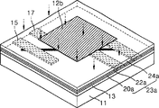
As shown in Figure 1, memory device comprises substrate 11 according to an embodiment of the invention, insulating barrier 13, source electrode 15 on the described insulating barrier 13 and drain electrode 17, carbon nano-tube 21, memory cell 23 and gate electrode 19, wherein, described insulating barrier 13 is deposited on the described substrate 11, described source electrode 15 and drain electrode 17 preset distance that is made of metal and separates each other, described carbon nano-tube 21 is connected described source electrode 15 and described drain electrode 17 and play the effect of electronics movable passageway, described described carbon nano-tube 21 of memory cell 23 contacts and store electrons electric charge (or hole charge), the described gate electrode 19 described memory cell 23 of contact are also controlled electronic motion.
In Fig. 1, source electrode 15 is installed on the substrate 11 with drain electrode 17.Yet source electrode 15 can be installed in the substrate 11 with drain electrode 17.In the case, carbon nano-tube 21 also is set in the substrate 11, perhaps is mounted to the inner surface of substrate 11 to contact.
Described substrate 11 is made by silicon usually, and the described insulating barrier 13 that is formed on the substrate 11 is made by silica.
Described carbon nano-tube 21 is allotropes of a kind of carbon, and it has a kind of honeycomb shape by carbon atom is mutually combined and forms.In other words, carbon nano-tube 21 has a kind of shape, in this shape, is wound into the circumference with nanometer grade diameter in conjunction with formed graphite flake by a plurality of carbon atoms.According to the winding angle and the structure of graphite flake, carbon nano-tube 21 or have metallic character or have characteristic of semiconductor.At current industrial circle, particularly field of nanometer technology, people are studying this characteristic of carbon nano-tube energetically.
Carbon nano-tube according to their electrical characteristics be divided into two kinds dissimilar.One type is metal carbon nanotube, and their electronic behavior is an ohmic properties, and is not subjected to the influence of grid voltage.Another kind of type is a semiconductor carbon nanometer tube, and their electronic behavior is non-ohmic properties, and influenced by grid voltage.
Used carbon nano-tube 21 is a kind of semiconductor carbon nanometer tubes in the memory device according to the embodiment of the invention.Be applied to voltage on the gate electrode 19 by change, control the electron stream that moves by carbon nano-tube 21, i.e. electric current.
Described carbon nano-tube 21 can be used method manufacturings such as arc discharge, laser evaporation, plasma enhanced chemical vapor deposition (PECVD), thermal chemical vapor deposition, vapor phase growth.
Fig. 2,3A and 3B illustrate first, second and the 3rd memory cell 23,25 and 35 that is adopted in the memory device according to an embodiment of the invention respectively.
As shown in Figure 2, first memory cell 23 that is adopted in memory device according to an embodiment of the invention comprises first and second dielectric films 20 and 24 and charge storage film 22.These charge storage film 22 stored charges, i.e. electronics or hole, and be inserted between first and second dielectric films 20 and 24.First and second dielectric films 20 and 24 are by silicon oxide sio
2Form, and charge storage film 22 is by silicon (Si) or silicon nitride (Si
3N
4) form.Particularly, Si
3N
4Film provides as the low-potential energy trap sites (low-potential trap site) that can store a plurality of electric charges.
Preferably, the thickness of whole first memory cell 23 is about 60nm, and the thickness of charge storage film 22 is about 15nm or littler.Confirm, when the thickness as the silicon fiml of charge storage film 22 or silicon nitride film is 100nm or more hour, it can store electrons.Preferably, described first dielectric film 20 is enough thin, so that the electric charge that receives from carbon nano-tube shown in Figure 1 21 is tunnelling easily, and described second dielectric film 24 is enough thick, be imported into wherein from the electric charge of gate electrode 19 preventing, and the electric charge that will be stored in the charge storage film 22 is preserved for a long time.Such as, first dielectric film 20 is the thick sull of 7nm, charge storage film 22 is the thick Si of 7nm
3N
4Film, and second dielectric film 24 is the thick sull of 14nm.Here, described first dielectric film 20, the thickness ratio that the charge storage film 22 and second dielectric film 24 form them is 1: 1: 2, feasible charge energy from carbon nano-tube 21 stably is stored in the charge storage film 22 for a long time.
Fig. 3 A is the cross-sectional view of second memory cell 25 that adopted in the memory device according to an embodiment of the invention.As shown in Figure 3A, second memory cell 25 comprises the 3rd dielectric film 29 and the perforated membrane 26 that contacts with described gate electrode 19 formation, and this perforated membrane 26 is formed at the below of the 3rd dielectric film 29, and has a plurality of nano dots 27 that filled up by charge storage material 28.
The 3rd dielectric film 29 can be formed by silica, and charge storage material 28 can be silicon or silicon nitride.Preferably, the 3rd dielectric film 29 is thicker than described perforated membrane 26, so that described charge storage material 28 stably can be kept in the nano dot 27.
Fig. 3 B is the cross-sectional view of the 3rd memory cell 35 that adopted in the memory device according to an embodiment of the invention.The structure of the 3rd memory cell 35 is, therein, also is formed with a dielectric film below the perforated membrane 26 of second memory cell 25.Thereby the 3rd memory cell 35 comprises the 4th dielectric film 34, have the perforated membrane 36 of a plurality of nano dots 37 that filled up by charge storage material 38 and pentasyllabic quatrain velum 34 '.Preferably, the 4th dielectric film 34 is enough thick, is imported into wherein from the electric charge of the gate electrode 19 of Fig. 1 preventing, and is stored in electric charge in the charge storage film 38 for a long time.Preferably, pentasyllabic quatrain velum 34 ' enough is thin, make from the electronics of carbon nano-tube 21 or hole can be easily tunnelling therein, and move in this perforated membrane 36.
Fig. 4 is scanning electron microscopy (SEM) photo of the 3rd memory cell 35 that adopts in the memory device according to an embodiment of the invention.In this SEM photo, the 4th dielectric film 34 is by SiO
2Form, perforated membrane 36 and pentasyllabic quatrain velum 34 ' by Al
2O
3Form, and charge storage material 38 is by Si (or Si
3N
4) form.
Fig. 5 A and 5B show the SEM photo that is connected source electrode 15 and the carbon nano-tube 21 of drain electrode 17 in the memory device according to an embodiment of the invention.Adopt the atomic energy microscope, the diameter that can measure this carbon nano-tube 21 is about 3nm.
Fig. 6 A to 6I is a perspective view, is used to illustrate the manufacture method of a kind of memory device that adopts first memory cell 23 according to an embodiment of the invention.At first, referring to Fig. 6 A,, on insulating barrier 13, generate carbon nano-tube 21 then at the upper surface depositing insulating layer 13 of substrate 11.Carbon nano-tube (CNT) powder with the CVD manufactured is dispersed in the chloroformic solution, then, and the several position place coating on insulating barrier 13 and dry.Fig. 6 A is illustrated in the formed single-root carbon nano-tube 21 in a position on the substrate 11.
Next, shown in Fig. 6 B, deposition is used to form the conductive material layer 14 of source electrode 15 and drain electrode 17 on insulating barrier 13, then, utilizes a mask 12a to come patterning conductive material layer 14 by the electron beam lithography method.Such as, conductive material layer 14 can be formed such as Au or Ti by a kind of metal.Preferably, source electrode 15 that after the mask composition, forms and drain electrode 17 by thermal annealing to reduce contact resistance.Such as, source electrode 15 and drain electrode 17 can be about 30 seconds of 600 ℃ of short annealings.Fig. 6 C illustrates source electrode 15 and the drain electrode 17 that forms by this way.
The technical process of Fig. 6 D to 6F explanation deposition first memory cell 23.Referring to Fig. 6 D, on source electrode 15 and drain electrode 17, be connected on the carbon nano-tube 21 of source electrode 15 and drain electrode 17 and on insulating barrier 13, sequentially deposit the first dielectric film 20a, charge storage film 22a and the second dielectric film 24a, thereby form memory cell 23a.Shown in Fig. 6 E, a mask 12b is set, and to its exposure, then, formed structure is developed (develop) on the formed structure of Fig. 6 D.Shown in Fig. 6 F, first memory cell 23 forms to contact with the upper surface of source electrode 15 and drain electrode 17 and the upper surface of carbon nano-tube 21.First memory cell 23 comprises first dielectric film of being made by oxide 20, by Si or Si
3N
4Charge storage film of making 22 and second dielectric film of making by oxide 24.By the CVD method, utilize SiH
4Gas and O
2The mixture of gas forms oxide-film, and by the CVD method, utilizes SiH
2Cl
2Gas and NH
3Gas forms Si
3N
4Film.
Fig. 6 G to 6I illustrates the process that forms gate electrode 19.Referring to Fig. 6 G, deposition is used to form the metal level 18 of gate electrode 19 with the coated carbon nanotube 21 and first memory cell 23 on insulating barrier 13.Shown in Fig. 6 H, on this metal level 18, mask 12c is set, under ultraviolet ray, to expose then, formed then structure is developed.After the step shown in Fig. 6 H, form the gate electrode 19 shown in Fig. 6 I.
Fig. 7 A to 7E illustrates the manufacture method of the 3rd memory cell 35 that is adopted in the memory device according to an embodiment of the invention.At first, shown in Fig. 7 A, pentasyllabic quatrain velum 34 ' oxidized with obtain thereon an oxide-film 36 '.Make formed structure oxidation and this structure of etching by powering up, just made perforated membrane 36, shown in Fig. 7 B with a plurality of nano dots 37.If pentasyllabic quatrain velum 34 ' made of aluminum, then this aluminium is dipped into sulfuric acid solution or phosphoric acid solution, and is powered oxidation, to form a plurality of nano dots 37.This oxidation is called as anodic oxidation.This aluminium is oxidized to aluminium oxide, and the volume of the aluminium that its volume ratio is original is big.
Shown in Fig. 7 C, adopt CVD or sputtering technology, with silicon or silicon nitride, promptly the material of charge storage film 22 fills up nano dot 37.After this, shown in Fig. 7 D, formed nano dot 37 can be assembled the perforated membrane 36 of electric charge with formation by dry etching.Then, shown in Fig. 7 E, the 4th dielectric film 34 is deposited on the perforated membrane 36, thereby has finished the manufacturing of the 3rd memory cell 35.In order to make the memory device that includes the 3rd memory cell 35, at first, according to forming carbon nano-tube 21 and source electrode 15 and drain electrode 17 shown in Fig. 6 A to 6C.Then, shown in Fig. 7 A to 7E, can on carbon nano-tube 21, form the 3rd memory cell 35.After this, shown in Fig. 6 G to 6I, form gate electrode 19.
Can use with the similar method of the manufacture method of the 3rd memory cell 35 and make second memory cell 25.As in forming the process of the 3rd memory cell 35, by complete oxidation pentasyllabic quatrain velum 34 ' form perforated membrane 26 with a plurality of nano dots 27.After this, nano dot 27 is filled up, on formed perforated membrane 26, deposit the 3rd dielectric film 29 then, thereby form second memory cell 25 as shown in Figure 3A with charge storage material 28.
In memory device according to an embodiment of the invention, if source electrode 15 is grounded, on drain electrode 17, apply positive drain voltage, then electronics is shifted to carbon nano-tube 21, thus electric current flows.At this moment, if will be higher than a pre-defined gate voltage of the drain voltage that is applied on the drain electrode 17 is applied on the gate electrode 19, then electronics is shifted to memory cell (23,25 or 35) from carbon nano-tube 21, tunnelling by first dielectric film 20 or pentasyllabic quatrain velum 34 ', and move to charge storage film 22 or nano dot 27 and 37.By suitably control gate pole tension and drain voltage, electronics is deposited in, is removed and flowed out charge storage film 22 and nano dot 27 and 37, thereby realizes record, elimination and the reproduction of data.
Fig. 8 A is a kind of plane graph of memory device according to an embodiment of the invention, following a plurality of source electrodes and a drain electrode and a carbon nano-tube that it comprises a single gate electrode and is positioned at gate electrode.Fig. 8 B is a picture, and a kind of carbon nano-tube passage of source electrode shown in the connection layout 8A (S) and drain electrode (D) is shown.
Memory device according to an embodiment of the invention, material, grid voltage and the source electrode-drain voltage of material and the thickness by the storage film of control store unit suitably, the diameter of each nano dot that is comprised in a plurality of nano dots in the perforated membrane and length, filled with nanotubes passage, this memory device can be used as volatile memory or nonvolatile memory.
Fig. 9 is in memory device according to an embodiment of the invention, when grid voltage when 0V changes to 10V, the electric current I sd between source electrode and the drain electrode is to the graph of a relation of the voltage Vsd between source electrode and the drain electrode.
Curve f
1Expression, when grid voltage was 0V, source electrode-drain current Isd was 0, and is irrelevant with the variation of source electrode-drain voltage Vsd.
Curve f
2Expression, when grid voltage is 10V, along with source electrode-drain voltage Vsd from 0 be increased to one on the occasion of, source electrode-drain current Isd is increased to about 1000nA from 0, but along with source electrode-drain voltage Vsd is reduced to a negative value from 0, source electrode-drain current Isd is reduced to pact-1000nA from 0.
If grid voltage is 0V when certain one source pole-drain voltage value, does not then have electronics to move between source electrode and drain electrode, thereby can not realize that data write.If grid voltage is greater than 0V, then source electrode-drain current begins to flow.Along with the increase of grid voltage,, just can realize storage by catching the electronics of predetermined quantity.
Figure 10 is in a kind of p type CNT field-effect transistor (FET), and the electric current I sd between source electrode and the drain electrode is to the graph of a relation of grid voltage Vg, and this FET has a charge storage film, the ONO film that this storage film is a 28nm.
As shown in figure 10, in p type CNT FET, along with the increase of the negative voltage of gate electrode, source electrode-drain current Isd increases, and when the voltage of gate electrode be on the occasion of the time, electric current I sd is reduced to several flying (femto) and pacifies (fA).When Vsd=1V, when the voltage of gate electrode from-when 4V changed to 4V, the ratio Ion/Ioff of on-state current Ion and open state current Ioff surpassed 10
5Measured open state current remains on several pA or littler.It is believed that, the electric current of off-state remain on a low value be by gate electrode in memory device the position and the high-breakdown-voltage of ONO film cause.Under the situation of flush memory device, threshold voltage increases along with the increase of ratio I on/Ioff, thereby has improved performance.
Figure 11 A demonstrates the thick memory cell (SiO of a kind of 7nm of having
2/ Si
3N
4/ SiO
2) current-voltage (I-V) characteristic of P type CNT memory device.Figure 11 B demonstrates the thick memory cell (SiO of a kind of 30nm of having
2/ Si
3N
4/ SiO
2) current-voltage (I-V) characteristic of N type CNT memory device.
Referring to Figure 11 A, the relative source electrode of the drain current Id-drain voltage Vsd in the P type CNT memory device and changing slightly.Yet, if when grid voltage Vg was the 2.5V left and right sides, drain current Id reduced sharp.
Referring to Figure 11 B, if grid voltage Vg is equal to or greater than 4V, then when Vsd=3V, the drain current Id in the N type CNT memory device shows clear and definite hysteresis.
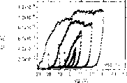
Figure 12 is for when applying different source electrode-drain voltage Vsd on a N type CNT memory device, the graph of a relation of drain current Id and grid voltage Vg, and grid voltage Vg is from 0V to 1V.Referring to Figure 12, the situation when n1 represents that Vsd is 0V, n2 represents that Vsd is-situation during 5V, and n3 represents that Vsd is-situation during 5.5V, and n4 represents that Vsd is-situation during 6V, and n5 represents Vsd is-situation during 6.5V.Can see that from n1 to n5 drain current Id increases and increases along with grid voltage Vg, and reaches capacity when the about 0.6V of Vg.
Suppose that h represents the thickness of memory cell, i.e. the thickness of ONO film, L and r represent the length and the radius of carbon nano-tube respectively, then the static capacity of this carbon nano-tube per unit length is expressed as formula 1:
C/L=2πεε
o/ln(2h/r) ……(1)
When the effective dielectric constant of this ONO film is-3, h is 30nm, and r is 1.5nm, and L is 1 μ m, when damaging grid voltage Vgd and being 2V, then draws 580 μ m according to formula 1
-1Hole density (P).Can calculate the hole mobility (μ of this CNT according to formula 2
h), formula 2 is:
μ
h=29cm
2/(V·S) ……(2)
Above-mentioned hole mobility (μ
h) greater than the hole mobility of a single-walled nanotube or the hole mobility of compound wall nanotube (MWNT).
Figure 13 is in memory device according to an embodiment of the invention, when drain current Id is 50nA consistently, and the graph of a relation of threshold voltage vt h and grid voltage Vg.When positive grid voltage increased, threshold voltage vt h increased, and this means that the hole from carbon nano-tube is injected into an ONO film and fills a trap sites.As seen from Figure 13, when grid voltage Vg when 0V increases to 7V, threshold voltage has increased about 60mV, finds that correspondingly the hole is by accurate quantization.
Figure 14 is illustrated in according to an embodiment of the invention in the memory device, the schematic diagram of the electric field between carbon nano-tube and the gate electrode, and the graph of a relation of the surface induction charge density (σ) at gate electrode place and the distance between CNT and the gate electrode.
Referring to Figure 14, grid voltage has formed a highfield around the surface of carbon nano-tube (CNT).When the diameter that is considered to a complete conductor and this CNT when this gate electrode was 3nm, the ONO film between this CNT and this gate electrode can be considered to an individual layer, and its effective dielectric constant is 3.So, can calculate electric field around this CNT.If grid voltage is 5V, the electric field that then calculates is 970V/ μ m, and one is enough to bring out the highfield of Fowller Nodheim tunneling.And if the tunneling electric charge flows along electric field line, the electric field strength that they calculate with distributing based on charge inducing is caught by nitride film pro rata.In the calculating of this electric field, all 70% of the tunnelling electric charges is consistent with the overall with of (FWHW) locating in half maximum (half maximum) of the peak value of charge density, and the thickness that inflow is included in the OHO film is in the nitride film of 14nm.As everyone knows, when the size of quantum dot (quantum dot) is equal to or less than 10nm, electric charge when room temperature by quantization.Referring to the curve chart of Figure 14, charge inducing density (σ) increases during near CNT.
Figure 15 is in memory device according to an embodiment of the invention, drain current Id and time relation figure, for example 100 seconds.The CHARGE DISTRIBUTION of one localization can make in the nitride film of the sensed ONO film of electric charge, this is because the carbon nano-tube of localization has high Electric Field Distribution, and the electric charge of being caught by the localized areas of ONO film can be dispersed to the zone that does not have stored charge.Yet as shown in figure 15, along with the past of time, it is constant that the total amount of electric current keeps.Thereby can learn that an electric charge capture position of the ONO film of CNT memory device of the present invention can be used as the quantum dot of flush memory device.
The invention provides the nonvolatile semiconductor memory member of a kind of CNT-FET of employing and ONO film, wherein, electric charge is stored in the trap bit of ONO film.Stored charge has the quantization voltage increment of about 60mV, this means that the ONO film has accurate quantized energy state.This quantization energy state is relevant with the high local electric field that and a nanoscale CNT passage interrelate, and is representing the CNT memory device as a kind of super-high density high-capacity flash memory.
Adopt carbon nano-tube to replace injecting raceway groove (implantationchannel) according to memory device according to the present invention and come dislocation charge between source electrode and drain electrode, and comprise charge storage film or have the perforated membrane of nano dot, and need not extra capacitor.
And, because adopted carbon nano-tube as the electronics movable passageway with high conductivity and high-termal conductivity, thus a kind of little transistor can be made, thereby can make high integrated, dynamical memory device.
Although the present invention has been carried out illustrating particularly and describing in conjunction with exemplary embodiment of the present invention, but should know, do not deviating under the situation by described claim institute's restricted portion and spirit of the present invention, those skilled in the art can do multiple variation on form and the details to it.
Generally speaking, memory device of the present invention comprises the small transistor that adopts a high conductance CNT and the memory cell of store electrons, thereby has high efficiency and high integration.
Claims (36)
1. carbon nano-tube memory device comprises:
Substrate;
Be arranged on the described substrate therebetween with having a predetermined space and be subjected to the source electrode and the drain electrode of a voltage;
Carbon nano-tube, it is connected described source electrode with drain electrode, and as the electric charge passage;
Memory cell, it is positioned at the top of described carbon nano-tube, and storage is from the electric charge of carbon nano-tube; And
Gate electrode, it forms to contact with the upper surface of described memory cell, flows into described charge storing unit quantity with control from described carbon nano-tube.
2. carbon nano-tube memory device according to claim 1, wherein said substrate is made by silicon.
3. carbon nano-tube memory device according to claim 2 wherein deposits silicon oxide film on described substrate.
4. carbon nano-tube memory device according to claim 1, wherein said memory cell comprises:
First dielectric film, it forms to contact with the upper surface of described carbon nano-tube;
Charge storage film, it is deposited on described first dielectric film, and stored charge; And
Second dielectric film, it is formed on the described charge storage film and with described gate electrode and contacts.
5. carbon nano-tube memory device according to claim 4, the thickness of wherein said first dielectric film equates with the thickness of described charge storage film.
6. carbon nano-tube memory device according to claim 4, the thickness of wherein said second dielectric film are the twice of the thickness of described charge storage film.
7. carbon nano-tube memory device according to claim 4, wherein said first and second dielectric films are formed by silica.
8. carbon nano-tube memory device according to claim 4, wherein said charge storage film is formed by one of silicon and silicon nitride.
9. carbon nano-tube memory device according to claim 4, the thickness of wherein said charge storage film are 15nm or littler.
10. carbon nano-tube memory device according to claim 4, wherein said charge storage film are perforated membrane, and it has a plurality of nano dots that filled up by charge storage material.
11. carbon nano-tube memory device according to claim 1, wherein said memory cell comprises:
The 3rd dielectric film, it forms to contact with the lower surface of described gate electrode; And
Perforated membrane, it is deposited over the following of described the 3rd dielectric film and contacts with described carbon nano-tube, and this perforated membrane has a plurality of nano dots that filled up by charge storage material.
12. carbon nano-tube memory device according to claim 11, the thickness of wherein said the 3rd dielectric film are the twice of described perforated membrane thickness.
13. carbon nano-tube memory device according to claim 11, the thickness of wherein said the 3rd dielectric film equates with the thickness of described perforated membrane.
14. carbon nano-tube memory device according to claim 11, wherein said the 3rd dielectric film is formed by silica.
15. according to claim 10 or 11 described carbon nano-tube memory devices, wherein said charge storage material is a kind of in silicon and the silicon nitride.
16. according to claim 10 or 11 described carbon nano-tube memory devices, wherein said perforated membrane is formed by aluminium oxide.
17. according to claim 10 or 11 described carbon nano-tube memory devices, the diameter of wherein said nano dot is 15nm or littler.
18. a method of making the carbon nano-tube memory device, this method comprises:
(a) carbon nano-tube on substrate, and formation and contacted source electrode of described carbon nano-tube and drain electrode make that the described carbon nano-tube between described source electrode and the drain electrode is used as the electric charge movable passageway;
(b) by on described carbon nano-tube, source electrode and drain electrode, sequentially depositing first dielectric film, charge storage film and second dielectric film, and adopt photoetching process that the structure of gained is formed pattern, thereby the formation memory cell, this memory cell contacts with described carbon nano-tube;
(c) by depositing metal layers on described second dielectric film and adopt photoetching process that the structure of gained is formed pattern, thereby form gate electrode, this gate electrode control flows into the amount of charge of described charge storage film from described carbon nano-tube.
19. method according to claim 18 wherein in step (a), forms insulating barrier on the upper surface of described substrate, and the described carbon nano-tube of growing on the upper surface of this insulating barrier.
20. method according to claim 19, wherein said substrate is formed by silicon, and described insulating barrier is formed by silica.
21., wherein in step (a), adopt the electron beam lithography method to form described source electrode and drain electrode according to claim 18 or 19 described methods.
22. method according to claim 18, wherein in step (b), described first dielectric film is deposited to the thickness that its thickness equals described charge storage film.
23. method according to claim 18, wherein in step (b), described second dielectric film is deposited to the twice that its thickness is described charge storage film thickness.
24. method according to claim 18, wherein said first and second dielectric films are formed by silica.
25. method according to claim 18, wherein said charge storage film is formed by one of silicon and silicon nitride.
26. method according to claim 18, the thickness of wherein said charge storage film are 15nm or littler.
27. a method of making the carbon nano-tube memory, this method comprises:
(a) source electrode and drain electrode that carbon nano-tube on substrate, and formation contacts with described carbon nano-tube make that the described carbon nano-tube between described source electrode and the drain electrode is used as the electric charge movable passageway;
(b) by deposition first dielectric film on the upper surface of described carbon nano-tube, source electrode and drain electrode, and anodic oxidation and described first dielectric film of etching, perforated membrane formed with a plurality of nano dots;
(c) by deposited charge storage medium on the upper surface of described perforated membrane, this charge storage material of etching fills up described nano dot with this charge storage material then;
(d) by deposition second dielectric film on the upper surface of described perforated membrane, and adopt photoetching process to make described first dielectric film, perforated membrane and second dielectric film form pattern, thereby form a memory cell; And
(e) by depositing metal layers on described second dielectric film and adopt photoetching process that the structure of gained is formed pattern, thereby form gate electrode, this gate electrode control flows into the amount of charge of described charge storage film from described carbon nano-tube.
28. method according to claim 27 wherein in step (a), forms insulating barrier on the upper surface of described substrate, and the described carbon nano-tube of growing on the upper surface of this insulating barrier.
29. method according to claim 28, wherein said substrate is formed by silicon, and described insulating barrier is formed by silica.
30., wherein in step (a), adopt electron beam lithography to form described source electrode and drain electrode according to claim 27 or 28 described methods.
31. method according to claim 27, wherein in step (d), described first dielectric film is deposited to the thickness that its thickness equals described perforated membrane.
32. method according to claim 27, wherein in step (d), described second dielectric film is deposited to the twice that its thickness is described perforated membrane thickness.
33. method according to claim 27, wherein said first and second dielectric films are formed by silica.
34. method according to claim 27, one of them forms wherein said charge storage material by silicon and silicon nitride.
35. method according to claim 27, the thickness of wherein said perforated membrane are 100nm or littler.
36. method according to claim 27, wherein in step (a), described whole first dielectric film is oxidized to form described perforated membrane with a plurality of nano dots.
Applications Claiming Priority (6)
| Application Number | Priority Date | Filing Date | Title |
|---|---|---|---|
| KR7709/2002 | 2002-02-09 | ||
| KR20020007709 | 2002-02-09 | ||
| KR7709/02 | 2002-02-09 | ||
| KR10-2002-0071398A KR100450825B1 (en) | 2002-02-09 | 2002-11-16 | Memory device utilizing carbon nano tube and Fabricating method thereof |
| KR71398/02 | 2002-11-16 | ||
| KR71398/2002 | 2002-11-16 |
Publications (2)
| Publication Number | Publication Date |
|---|---|
| CN1450643A CN1450643A (en) | 2003-10-22 |
| CN1287459C true CN1287459C (en) | 2006-11-29 |
Family
ID=36571480
Family Applications (1)
| Application Number | Title | Priority Date | Filing Date |
|---|---|---|---|
| CNB031285929A Expired - Fee Related CN1287459C (en) | 2002-02-09 | 2003-02-09 | Memory device utilizing carbon nanotubes and method of fabricating the memory device |
Country Status (5)
| Country | Link |
|---|---|
| US (2) | US7015500B2 (en) |
| EP (1) | EP1341184B1 (en) |
| JP (1) | JP5165828B2 (en) |
| CN (1) | CN1287459C (en) |
| DE (1) | DE60301582T2 (en) |
Cited By (1)
| Publication number | Priority date | Publication date | Assignee | Title |
|---|---|---|---|---|
| CN104934536A (en) * | 2015-06-04 | 2015-09-23 | 复旦大学 | Organic thin-film memory doped with carbon nano tubes |
Families Citing this family (141)
| Publication number | Priority date | Publication date | Assignee | Title |
|---|---|---|---|---|
| US6835591B2 (en) * | 2001-07-25 | 2004-12-28 | Nantero, Inc. | Methods of nanotube films and articles |
| US6706402B2 (en) | 2001-07-25 | 2004-03-16 | Nantero, Inc. | Nanotube films and articles |
| US6574130B2 (en) * | 2001-07-25 | 2003-06-03 | Nantero, Inc. | Hybrid circuit having nanotube electromechanical memory |
| US6919592B2 (en) * | 2001-07-25 | 2005-07-19 | Nantero, Inc. | Electromechanical memory array using nanotube ribbons and method for making same |
| US6643165B2 (en) | 2001-07-25 | 2003-11-04 | Nantero, Inc. | Electromechanical memory having cell selection circuitry constructed with nanotube technology |
| US7176505B2 (en) * | 2001-12-28 | 2007-02-13 | Nantero, Inc. | Electromechanical three-trace junction devices |
| US6784028B2 (en) * | 2001-12-28 | 2004-08-31 | Nantero, Inc. | Methods of making electromechanical three-trace junction devices |
| DE60301582T2 (en) * | 2002-02-09 | 2006-06-22 | Samsung Electronics Co., Ltd., Suwon | Carbon nanotube storage device and method of manufacturing the storage device |
| US7335395B2 (en) * | 2002-04-23 | 2008-02-26 | Nantero, Inc. | Methods of using pre-formed nanotubes to make carbon nanotube films, layers, fabrics, ribbons, elements and articles |
| JP4416376B2 (en) * | 2002-05-13 | 2010-02-17 | 富士通株式会社 | Semiconductor device and manufacturing method thereof |
| KR100790859B1 (en) * | 2002-11-15 | 2008-01-03 | 삼성전자주식회사 | Nonvolatile memory device utilizing vertical nanotube |
| US7560136B2 (en) * | 2003-01-13 | 2009-07-14 | Nantero, Inc. | Methods of using thin metal layers to make carbon nanotube films, layers, fabrics, ribbons, elements and articles |
| WO2004088719A2 (en) * | 2003-03-28 | 2004-10-14 | Nantero, Inc. | Nanotube-on-gate fet structures and applications |
| US7294877B2 (en) | 2003-03-28 | 2007-11-13 | Nantero, Inc. | Nanotube-on-gate FET structures and applications |
| US7780918B2 (en) * | 2003-05-14 | 2010-08-24 | Nantero, Inc. | Sensor platform using a horizontally oriented nanotube element |
| US6982903B2 (en) * | 2003-06-09 | 2006-01-03 | Nantero, Inc. | Field effect devices having a source controlled via a nanotube switching element |
| US7274064B2 (en) * | 2003-06-09 | 2007-09-25 | Nanatero, Inc. | Non-volatile electromechanical field effect devices and circuits using same and methods of forming same |
| WO2005017967A2 (en) * | 2003-08-13 | 2005-02-24 | Nantero, Inc. | Nanotube device structure and methods of fabrication |
| JP2007502545A (en) * | 2003-08-13 | 2007-02-08 | ナンテロ,インク. | Nanotube-based exchange element with a plurality of control devices and circuit produced from said element |
| US7115960B2 (en) * | 2003-08-13 | 2006-10-03 | Nantero, Inc. | Nanotube-based switching elements |
| US7289357B2 (en) | 2003-08-13 | 2007-10-30 | Nantero, Inc. | Isolation structure for deflectable nanotube elements |
| US7583526B2 (en) | 2003-08-13 | 2009-09-01 | Nantero, Inc. | Random access memory including nanotube switching elements |
| CN101562049B (en) * | 2003-08-13 | 2012-09-05 | 南泰若股份有限公司 | Nanotube-based switching elements with multiple controls and circuits made thereof |
| US7374793B2 (en) | 2003-12-11 | 2008-05-20 | International Business Machines Corporation | Methods and structures for promoting stable synthesis of carbon nanotubes |
| US7038299B2 (en) * | 2003-12-11 | 2006-05-02 | International Business Machines Corporation | Selective synthesis of semiconducting carbon nanotubes |
| DE102004001340A1 (en) * | 2004-01-08 | 2005-08-04 | Infineon Technologies Ag | Method for fabricating a nanoelement field effect transistor, nanoelement field effect transistor and nanoelement arrangement |
| US7211844B2 (en) | 2004-01-29 | 2007-05-01 | International Business Machines Corporation | Vertical field effect transistors incorporating semiconducting nanotubes grown in a spacer-defined passage |
| US20050167655A1 (en) * | 2004-01-29 | 2005-08-04 | International Business Machines Corporation | Vertical nanotube semiconductor device structures and methods of forming the same |
| US7528437B2 (en) | 2004-02-11 | 2009-05-05 | Nantero, Inc. | EEPROMS using carbon nanotubes for cell storage |
| US7829883B2 (en) * | 2004-02-12 | 2010-11-09 | International Business Machines Corporation | Vertical carbon nanotube field effect transistors and arrays |
| KR100694426B1 (en) * | 2004-02-16 | 2007-03-12 | 주식회사 하이닉스반도체 | Nano tube cell and memory device using the same |
| KR100709462B1 (en) * | 2004-02-16 | 2007-04-18 | 주식회사 하이닉스반도체 | Memory device using multiple layer nano tube cell |
| KR100709463B1 (en) * | 2004-02-16 | 2007-04-18 | 주식회사 하이닉스반도체 | Memory device using nano tube cell |
| US7709880B2 (en) * | 2004-06-09 | 2010-05-04 | Nantero, Inc. | Field effect devices having a gate controlled via a nanotube switching element |
| US7330709B2 (en) * | 2004-06-18 | 2008-02-12 | Nantero, Inc. | Receiver circuit using nanotube-based switches and logic |
| US7164744B2 (en) * | 2004-06-18 | 2007-01-16 | Nantero, Inc. | Nanotube-based logic driver circuits |
| US7288970B2 (en) * | 2004-06-18 | 2007-10-30 | Nantero, Inc. | Integrated nanotube and field effect switching device |
| US7161403B2 (en) * | 2004-06-18 | 2007-01-09 | Nantero, Inc. | Storage elements using nanotube switching elements |
| US7167026B2 (en) * | 2004-06-18 | 2007-01-23 | Nantero, Inc. | Tri-state circuit using nanotube switching elements |
| US7652342B2 (en) | 2004-06-18 | 2010-01-26 | Nantero, Inc. | Nanotube-based transfer devices and related circuits |
| US7329931B2 (en) * | 2004-06-18 | 2008-02-12 | Nantero, Inc. | Receiver circuit using nanotube-based switches and transistors |
| US7109546B2 (en) | 2004-06-29 | 2006-09-19 | International Business Machines Corporation | Horizontal memory gain cells |
| US9231201B2 (en) * | 2004-06-30 | 2016-01-05 | Nxp B.V. | Electric device with a layer of conductive material contacted by nanowires |
| US6955937B1 (en) * | 2004-08-12 | 2005-10-18 | Lsi Logic Corporation | Carbon nanotube memory cell for integrated circuit structure with removable side spacers to permit access to memory cell and process for forming such memory cell |
| US8471238B2 (en) * | 2004-09-16 | 2013-06-25 | Nantero Inc. | Light emitters using nanotubes and methods of making same |
| US7233071B2 (en) | 2004-10-04 | 2007-06-19 | International Business Machines Corporation | Low-k dielectric layer based upon carbon nanostructures |
| US7567414B2 (en) * | 2004-11-02 | 2009-07-28 | Nantero, Inc. | Nanotube ESD protective devices and corresponding nonvolatile and volatile nanotube switches |
| US20100147657A1 (en) * | 2004-11-02 | 2010-06-17 | Nantero, Inc. | Nanotube esd protective devices and corresponding nonvolatile and volatile nanotube switches |
| KR100657908B1 (en) * | 2004-11-03 | 2006-12-14 | 삼성전자주식회사 | Memory device having molecular absorption layer |
| US7634337B2 (en) * | 2004-12-29 | 2009-12-15 | Snap-On Incorporated | Vehicle or engine diagnostic systems with advanced non-volatile memory |
| US7937198B2 (en) * | 2004-12-29 | 2011-05-03 | Snap-On Incorporated | Vehicle or engine diagnostic systems supporting fast boot and reprogramming |
| US8362525B2 (en) * | 2005-01-14 | 2013-01-29 | Nantero Inc. | Field effect device having a channel of nanofabric and methods of making same |
| US7598544B2 (en) * | 2005-01-14 | 2009-10-06 | Nanotero, Inc. | Hybrid carbon nanotude FET(CNFET)-FET static RAM (SRAM) and method of making same |
| KR100682925B1 (en) * | 2005-01-26 | 2007-02-15 | 삼성전자주식회사 | Multi-bit non-volatile memory device, and method of operating the same |
| KR101078125B1 (en) * | 2005-02-07 | 2011-10-28 | 삼성전자주식회사 | Nonvolatile Nano-channel Memory Device using Mesoporous Material |
| US7824946B1 (en) | 2005-03-11 | 2010-11-02 | Nantero, Inc. | Isolated metal plug process for use in fabricating carbon nanotube memory cells |
| US9287356B2 (en) * | 2005-05-09 | 2016-03-15 | Nantero Inc. | Nonvolatile nanotube diodes and nonvolatile nanotube blocks and systems using same and methods of making same |
| US9390790B2 (en) | 2005-04-05 | 2016-07-12 | Nantero Inc. | Carbon based nonvolatile cross point memory incorporating carbon based diode select devices and MOSFET select devices for memory and logic applications |
| US8000127B2 (en) | 2009-08-12 | 2011-08-16 | Nantero, Inc. | Method for resetting a resistive change memory element |
| US7782650B2 (en) * | 2005-05-09 | 2010-08-24 | Nantero, Inc. | Nonvolatile nanotube diodes and nonvolatile nanotube blocks and systems using same and methods of making same |
| US9911743B2 (en) * | 2005-05-09 | 2018-03-06 | Nantero, Inc. | Nonvolatile nanotube diodes and nonvolatile nanotube blocks and systems using same and methods of making same |
| US7835170B2 (en) * | 2005-05-09 | 2010-11-16 | Nantero, Inc. | Memory elements and cross point switches and arrays of same using nonvolatile nanotube blocks |
| US7394687B2 (en) | 2005-05-09 | 2008-07-01 | Nantero, Inc. | Non-volatile-shadow latch using a nanotube switch |
| US8513768B2 (en) * | 2005-05-09 | 2013-08-20 | Nantero Inc. | Nonvolatile nanotube diodes and nonvolatile nanotube blocks and systems using same and methods of making same |
| US8008745B2 (en) * | 2005-05-09 | 2011-08-30 | Nantero, Inc. | Latch circuits and operation circuits having scalable nonvolatile nanotube switches as electronic fuse replacement elements |
| CN101484997B (en) * | 2005-05-09 | 2011-05-18 | 南泰若股份有限公司 | Memory arrays using nanotube articles with reprogrammable resistance |
| US7781862B2 (en) | 2005-05-09 | 2010-08-24 | Nantero, Inc. | Two-terminal nanotube devices and systems and methods of making same |
| US7479654B2 (en) | 2005-05-09 | 2009-01-20 | Nantero, Inc. | Memory arrays using nanotube articles with reprogrammable resistance |
| US8183665B2 (en) * | 2005-11-15 | 2012-05-22 | Nantero Inc. | Nonvolatile nanotube diodes and nonvolatile nanotube blocks and systems using same and methods of making same |
| US9196615B2 (en) * | 2005-05-09 | 2015-11-24 | Nantero Inc. | Nonvolatile nanotube diodes and nonvolatile nanotube blocks and systems using same and methods of making same |
| US8217490B2 (en) * | 2005-05-09 | 2012-07-10 | Nantero Inc. | Nonvolatile nanotube diodes and nonvolatile nanotube blocks and systems using same and methods of making same |
| US8102018B2 (en) * | 2005-05-09 | 2012-01-24 | Nantero Inc. | Nonvolatile resistive memories having scalable two-terminal nanotube switches |
| TWI324773B (en) | 2005-05-09 | 2010-05-11 | Nantero Inc | Non-volatile shadow latch using a nanotube switch |
| US8013363B2 (en) * | 2005-05-09 | 2011-09-06 | Nantero, Inc. | Nonvolatile nanotube diodes and nonvolatile nanotube blocks and systems using same and methods of making same |
| US7598127B2 (en) | 2005-05-12 | 2009-10-06 | Nantero, Inc. | Nanotube fuse structure |
| US7575693B2 (en) | 2005-05-23 | 2009-08-18 | Nantero, Inc. | Method of aligning nanotubes and wires with an etched feature |
| KR100755367B1 (en) | 2005-06-08 | 2007-09-04 | 삼성전자주식회사 | Nano-line semiconductor device having a cylindrical gate and fabrication method thereof |
| US7915122B2 (en) * | 2005-06-08 | 2011-03-29 | Nantero, Inc. | Self-aligned cell integration scheme |
| US7541216B2 (en) * | 2005-06-09 | 2009-06-02 | Nantero, Inc. | Method of aligning deposited nanotubes onto an etched feature using a spacer |
| WO2007002297A2 (en) | 2005-06-24 | 2007-01-04 | Crafts Douglas E | Temporary planar electrical contact device and method using vertically-compressible nanotube contact structures |
| DE602005023596D1 (en) * | 2005-07-08 | 2010-10-28 | St Microelectronics Srl | Method for realizing an electrical connection in an electronic semiconductor device between a nanometric circuit architecture and standard electronic components |
| US7687841B2 (en) * | 2005-08-02 | 2010-03-30 | Micron Technology, Inc. | Scalable high performance carbon nanotube field effect transistor |
| US7485908B2 (en) * | 2005-08-18 | 2009-02-03 | United States Of America As Represented By The Secretary Of The Air Force | Insulated gate silicon nanowire transistor and method of manufacture |
| EP1763037A1 (en) | 2005-09-08 | 2007-03-14 | STMicroelectronics S.r.l. | Nanotube memory cell with floating gate based on passivated nanoparticles and manufacturing process thereof |
| US7342277B2 (en) * | 2005-11-21 | 2008-03-11 | Intel Corporation | Transistor for non volatile memory devices having a carbon nanotube channel and electrically floating quantum dots in its gate dielectric |
| US7385839B2 (en) * | 2005-12-01 | 2008-06-10 | International Business Machines Corporation | Memory devices using carbon nanotube (CNT) technologies |
| US20070183189A1 (en) * | 2006-02-08 | 2007-08-09 | Thomas Nirschl | Memory having nanotube transistor access device |
| US7439594B2 (en) | 2006-03-16 | 2008-10-21 | Micron Technology, Inc. | Stacked non-volatile memory with silicon carbide-based amorphous silicon thin film transistors |
| US7615492B2 (en) * | 2006-07-21 | 2009-11-10 | Atomic Energy Council - Institute Of Nuclear Energy Research | Preparing method of CNT-based semiconductor sensitized solar cell |
| EP2104109A1 (en) * | 2006-08-08 | 2009-09-23 | Nantero, Inc. | Nonvolatile resistive memories, latch circuits, and operation circuits having scalable two-terminal nanotube switches |
| US7731503B2 (en) * | 2006-08-21 | 2010-06-08 | Formfactor, Inc. | Carbon nanotube contact structures |
| EP1900681B1 (en) * | 2006-09-15 | 2017-03-15 | Imec | Tunnel Field-Effect Transistors based on silicon nanowires |
| US8130007B2 (en) * | 2006-10-16 | 2012-03-06 | Formfactor, Inc. | Probe card assembly with carbon nanotube probes having a spring mechanism therein |
| US8354855B2 (en) * | 2006-10-16 | 2013-01-15 | Formfactor, Inc. | Carbon nanotube columns and methods of making and using carbon nanotube columns as probes |
| US9806273B2 (en) * | 2007-01-03 | 2017-10-31 | The United States Of America As Represented By The Secretary Of The Army | Field effect transistor array using single wall carbon nano-tubes |
| GB0801494D0 (en) | 2007-02-23 | 2008-03-05 | Univ Ind & Acad Collaboration | Nonvolatile memory electronic device using nanowire used as charge channel and nanoparticles used as charge trap and method for manufacturing the same |
| KR100955879B1 (en) | 2007-02-26 | 2010-05-04 | 고려대학교 산학협력단 | Nonvolatile memory electronic device and Method for fabricating the same |
| WO2008112764A1 (en) | 2007-03-12 | 2008-09-18 | Nantero, Inc. | Electromagnetic and thermal sensors using carbon nanotubes and methods of making same |
| KR101375833B1 (en) * | 2007-05-03 | 2014-03-18 | 삼성전자주식회사 | Field effect transistor having germanium nanorod and method of manufacturing the same |
| WO2009005908A2 (en) * | 2007-05-22 | 2009-01-08 | Nantero, Inc. | Triodes using nanofabric articles and methods of making the same |
| US8134220B2 (en) | 2007-06-22 | 2012-03-13 | Nantero Inc. | Two-terminal nanotube devices including a nanotube bridge and methods of making same |
| JP5227660B2 (en) * | 2007-07-11 | 2013-07-03 | 日精樹脂工業株式会社 | Method for producing carbon nanocomposite |
| KR101497744B1 (en) * | 2007-09-10 | 2015-03-02 | 유니버시티 오브 플로리다 리서치 파운데이션, 인크. | Nanotube enabled, gate-voltage controlled light emitting diodes |
| US8043978B2 (en) * | 2007-10-11 | 2011-10-25 | Riken | Electronic device and method for producing electronic device |
| US8149007B2 (en) * | 2007-10-13 | 2012-04-03 | Formfactor, Inc. | Carbon nanotube spring contact structures with mechanical and electrical components |
| US8063430B2 (en) * | 2007-10-18 | 2011-11-22 | Samsung Electronics Co., Ltd. | Semiconductor devices and methods of manufacturing and operating same |
| EP2062515B1 (en) * | 2007-11-20 | 2012-08-29 | So, Kwok Kuen | Bowl and basket assembly and salad spinner incorporating such an assembly |
| US7482652B1 (en) * | 2008-01-02 | 2009-01-27 | International Business Machines Corporation | Multiwalled carbon nanotube memory device |
| US7786466B2 (en) * | 2008-01-11 | 2010-08-31 | International Business Machines Corporation | Carbon nanotube based integrated semiconductor circuit |
| KR100930997B1 (en) | 2008-01-22 | 2009-12-10 | 한국화학연구원 | Carbon Nanotube Transistor Manufacturing Method and Carbon Nanotube Transistor |
| WO2010008624A2 (en) * | 2008-03-25 | 2010-01-21 | Nantero, Inc. | Carbon nanotube-based neural networks and methods of making and using same |
| US8587989B2 (en) * | 2008-06-20 | 2013-11-19 | Nantero Inc. | NRAM arrays with nanotube blocks, nanotube traces, and nanotube planes and methods of making same |
| US9263126B1 (en) | 2010-09-01 | 2016-02-16 | Nantero Inc. | Method for dynamically accessing and programming resistive change element arrays |
| US8541843B2 (en) | 2008-08-14 | 2013-09-24 | Nantero Inc. | Nonvolatile nanotube programmable logic devices and a nonvolatile nanotube field programmable gate array using same |
| CN101354913B (en) * | 2008-09-05 | 2010-06-02 | 北京大学 | Molecular level memory unit for enclosed type double-layer nanometer carbon tube |
| KR101491714B1 (en) * | 2008-09-16 | 2015-02-16 | 삼성전자주식회사 | Semiconductor devices and method of fabricating the same |
| US7915637B2 (en) | 2008-11-19 | 2011-03-29 | Nantero, Inc. | Switching materials comprising mixed nanoscopic particles and carbon nanotubes and method of making and using the same |
| US8272124B2 (en) * | 2009-04-03 | 2012-09-25 | Formfactor, Inc. | Anchoring carbon nanotube columns |
| US20100252317A1 (en) * | 2009-04-03 | 2010-10-07 | Formfactor, Inc. | Carbon nanotube contact structures for use with semiconductor dies and other electronic devices |
| US8574673B2 (en) | 2009-07-31 | 2013-11-05 | Nantero Inc. | Anisotropic nanotube fabric layers and films and methods of forming same |
| US8128993B2 (en) * | 2009-07-31 | 2012-03-06 | Nantero Inc. | Anisotropic nanotube fabric layers and films and methods of forming same |
| TWI488206B (en) * | 2009-08-07 | 2015-06-11 | Nantero Inc | Nanotube esd protective devices and corresponding nonvolatile and volatile nanotube switches |
| US9099537B2 (en) * | 2009-08-28 | 2015-08-04 | International Business Machines Corporation | Selective nanotube growth inside vias using an ion beam |
| US8351239B2 (en) * | 2009-10-23 | 2013-01-08 | Nantero Inc. | Dynamic sense current supply circuit and associated method for reading and characterizing a resistive memory array |
| US8222704B2 (en) * | 2009-12-31 | 2012-07-17 | Nantero, Inc. | Compact electrical switching devices with nanotube elements, and methods of making same |
| US9362390B2 (en) | 2010-02-22 | 2016-06-07 | Nantero, Inc. | Logic elements comprising carbon nanotube field effect transistor (CNTFET) devices and methods of making same |
| KR101129930B1 (en) * | 2010-03-09 | 2012-03-27 | 주식회사 하이닉스반도체 | Semiconductor device and method for forming the same |
| US8872176B2 (en) | 2010-10-06 | 2014-10-28 | Formfactor, Inc. | Elastic encapsulated carbon nanotube based electrical contacts |
| US8492748B2 (en) * | 2011-06-27 | 2013-07-23 | International Business Machines Corporation | Collapsable gate for deposited nanostructures |
| US9825154B2 (en) * | 2011-11-28 | 2017-11-21 | Michigan Technological University | Room temperature tunneling switches and methods of making and using the same |
| EP2915161B1 (en) | 2012-11-05 | 2020-08-19 | University of Florida Research Foundation, Inc. | Brightness compensation in a display |
| US9007732B2 (en) | 2013-03-15 | 2015-04-14 | Nantero Inc. | Electrostatic discharge protection circuits using carbon nanotube field effect transistor (CNTFET) devices and methods of making same |
| DE102013204546A1 (en) * | 2013-03-15 | 2014-09-18 | Carl Zeiss Smt Gmbh | Optical component |
| CN104779346B (en) * | 2014-01-15 | 2017-04-12 | 清华大学 | Preparation method of phase change storage unit |
| US9299430B1 (en) | 2015-01-22 | 2016-03-29 | Nantero Inc. | Methods for reading and programming 1-R resistive change element arrays |
| US9947400B2 (en) | 2016-04-22 | 2018-04-17 | Nantero, Inc. | Methods for enhanced state retention within a resistive change cell |
| US9941001B2 (en) | 2016-06-07 | 2018-04-10 | Nantero, Inc. | Circuits for determining the resistive states of resistive change elements |
| US9934848B2 (en) | 2016-06-07 | 2018-04-03 | Nantero, Inc. | Methods for determining the resistive states of resistive change elements |
| US10355206B2 (en) | 2017-02-06 | 2019-07-16 | Nantero, Inc. | Sealed resistive change elements |
| CN108903924B (en) * | 2018-07-03 | 2021-02-19 | 浙江理工大学 | Bracelet wearing device and method adopting static tremor signal |
| CN113053942B (en) * | 2021-03-15 | 2021-11-23 | 中国电子科技集团公司第五十八研究所 | High-radiation-resistance magnetic random access memory device and preparation method thereof |
Family Cites Families (9)
| Publication number | Priority date | Publication date | Assignee | Title |
|---|---|---|---|---|
| US6348711B1 (en) * | 1998-05-20 | 2002-02-19 | Saifun Semiconductors Ltd. | NROM cell with self-aligned programming and erasure areas |
| US6203864B1 (en) * | 1998-06-08 | 2001-03-20 | Nec Corporation | Method of forming a heterojunction of a carbon nanotube and a different material, method of working a filament of a nanotube |
| US6361861B2 (en) * | 1999-06-14 | 2002-03-26 | Battelle Memorial Institute | Carbon nanotubes on a substrate |
| US7335603B2 (en) * | 2000-02-07 | 2008-02-26 | Vladimir Mancevski | System and method for fabricating logic devices comprising carbon nanotube transistors |
| US6798000B2 (en) * | 2000-07-04 | 2004-09-28 | Infineon Technologies Ag | Field effect transistor |
| EP1170799A3 (en) * | 2000-07-04 | 2009-04-01 | Infineon Technologies AG | Electronic device and method of manufacture of an electronic device |
| DE10134866B4 (en) * | 2000-07-18 | 2005-08-11 | Lg Electronics Inc. | Method of horizontally growing carbon nanotubes and field effect transistor using the process grown carbon nanotubes |
| US6423583B1 (en) * | 2001-01-03 | 2002-07-23 | International Business Machines Corporation | Methodology for electrically induced selective breakdown of nanotubes |
| DE60301582T2 (en) * | 2002-02-09 | 2006-06-22 | Samsung Electronics Co., Ltd., Suwon | Carbon nanotube storage device and method of manufacturing the storage device |
-
2003
- 2003-02-07 DE DE60301582T patent/DE60301582T2/en not_active Expired - Lifetime
- 2003-02-07 EP EP03250805A patent/EP1341184B1/en not_active Expired - Fee Related
- 2003-02-07 JP JP2003030273A patent/JP5165828B2/en not_active Expired - Fee Related
- 2003-02-09 CN CNB031285929A patent/CN1287459C/en not_active Expired - Fee Related
- 2003-02-10 US US10/361,024 patent/US7015500B2/en not_active Expired - Fee Related
-
2006
- 2006-02-13 US US11/352,310 patent/US7378328B2/en not_active Expired - Fee Related
Cited By (1)
| Publication number | Priority date | Publication date | Assignee | Title |
|---|---|---|---|---|
| CN104934536A (en) * | 2015-06-04 | 2015-09-23 | 复旦大学 | Organic thin-film memory doped with carbon nano tubes |
Also Published As
| Publication number | Publication date |
|---|---|
| DE60301582D1 (en) | 2005-10-20 |
| EP1341184B1 (en) | 2005-09-14 |
| CN1450643A (en) | 2003-10-22 |
| JP5165828B2 (en) | 2013-03-21 |
| US20030170930A1 (en) | 2003-09-11 |
| US7378328B2 (en) | 2008-05-27 |
| EP1341184A1 (en) | 2003-09-03 |
| US7015500B2 (en) | 2006-03-21 |
| US20060252276A1 (en) | 2006-11-09 |
| DE60301582T2 (en) | 2006-06-22 |
| JP2003264249A (en) | 2003-09-19 |
Similar Documents
| Publication | Publication Date | Title |
|---|---|---|
| CN1287459C (en) | Memory device utilizing carbon nanotubes and method of fabricating the memory device | |
| JP4227504B2 (en) | Memory device using nanotubes | |
| US7608883B2 (en) | Transistor for non volatile memory devices having a carbon nanotube channel and electrically floating quantum dots in its gate dielectric | |
| KR102144171B1 (en) | Vertically Integrated 3-Dimensional Flash Memory for High Reliable Flash Memory and Fabrication Method Thereof | |
| JP2011507230A (en) | Memory cell and manufacturing method thereof | |
| JP5196500B2 (en) | Storage element and reading method thereof | |
| US7332740B2 (en) | Memory device having molecular adsorption layer | |
| KR100450825B1 (en) | Memory device utilizing carbon nano tube and Fabricating method thereof | |
| US10636810B2 (en) | Vertically-integrated 3-dimensional flash memory for high reliable flash memory and fabrication method thereof | |
| Rispal et al. | Large-Scale In Situ Fabrication of Voltage-Programmable Dual-Layer High-$\kappa $ Dielectric Carbon Nanotube Memory Devices With High On/Off Ratio | |
| US7968398B2 (en) | Method for producing a floating gate with an alternation of lines of first and second materials | |
| Huang et al. | Silicon Nanowire Charge‐Trap Memory Incorporating Self‐Assembled Iron Oxide Quantum Dots | |
| JP2011096784A (en) | Transistor, planar element, and method of manufacturing them | |
| US7998850B2 (en) | Semiconductor device and method for manufacturing the same | |
| KR100744959B1 (en) | Organic Semiconductor Devices and Fabrication Methods of the same | |
| KR101823261B1 (en) | Non-volatile memory device and method of manufacturing the same | |
| KR100683799B1 (en) | Memory device and organic thin film transistor | |
| Wang et al. | Iridium Nanocrystal Thin-Film Transistor Nonvolatile Memory with Si3N4/SiO2 Stack of Asymmetric Tunnel Barrier | |
| Zhou et al. | Flexible Floating Gate Memory | |
| JP2006294859A (en) | Organic fet and its manufacturing method | |
| Li et al. | Silicon Nanowire‐Based Nonvolatile Memory Cells: Progress and Prospects | |
| Richter et al. | Measurements for the reliability and electrical characterization of semiconductor nanowires |
Legal Events
| Date | Code | Title | Description |
|---|---|---|---|
| C06 | Publication | ||
| PB01 | Publication | ||
| C10 | Entry into substantive examination | ||
| SE01 | Entry into force of request for substantive examination | ||
| C14 | Grant of patent or utility model | ||
| GR01 | Patent grant | ||
| CF01 | Termination of patent right due to non-payment of annual fee |
Granted publication date: 20061129 Termination date: 20160209 |
|
| CF01 | Termination of patent right due to non-payment of annual fee |