CN1282128C - Image processing device and method - Google Patents
Image processing device and method Download PDFInfo
- Publication number
- CN1282128C CN1282128C CNB02804889XA CN02804889A CN1282128C CN 1282128 C CN1282128 C CN 1282128C CN B02804889X A CNB02804889X A CN B02804889XA CN 02804889 A CN02804889 A CN 02804889A CN 1282128 C CN1282128 C CN 1282128C
- Authority
- CN
- China
- Prior art keywords
- data
- processing
- operational processes
- filtering
- circuit
- Prior art date
- Legal status (The legal status is an assumption and is not a legal conclusion. Google has not performed a legal analysis and makes no representation as to the accuracy of the status listed.)
- Expired - Fee Related
Links
- 238000012545 processing Methods 0.000 title claims abstract description 202
- 238000000034 method Methods 0.000 title claims abstract description 169
- 238000001914 filtration Methods 0.000 claims abstract description 76
- 230000001419 dependent effect Effects 0.000 claims description 13
- 238000003672 processing method Methods 0.000 claims description 5
- 238000012360 testing method Methods 0.000 abstract description 9
- 108090000237 interleukin-24 Proteins 0.000 abstract description 2
- 101001139126 Homo sapiens Krueppel-like factor 6 Proteins 0.000 abstract 1
- 101000710013 Homo sapiens Reversion-inducing cysteine-rich protein with Kazal motifs Proteins 0.000 abstract 1
- 238000005516 engineering process Methods 0.000 description 8
- 238000000547 structure data Methods 0.000 description 8
- 101000870945 Homo sapiens Ras guanyl-releasing protein 3 Proteins 0.000 description 7
- 102100033450 Ras guanyl-releasing protein 3 Human genes 0.000 description 7
- 101100441251 Arabidopsis thaliana CSP2 gene Proteins 0.000 description 6
- 101100033098 Arabidopsis thaliana RBG2 gene Proteins 0.000 description 6
- 102100034032 Cytohesin-3 Human genes 0.000 description 6
- 101710160297 Cytohesin-3 Proteins 0.000 description 6
- 101100511870 Fagus sylvatica LSM4 gene Proteins 0.000 description 6
- 101150095494 GRP2 gene Proteins 0.000 description 6
- 230000000153 supplemental effect Effects 0.000 description 6
- 238000005286 illumination Methods 0.000 description 5
- 230000009183 running Effects 0.000 description 3
- 230000005540 biological transmission Effects 0.000 description 2
- 238000013461 design Methods 0.000 description 2
- 230000006870 function Effects 0.000 description 2
- 230000004807 localization Effects 0.000 description 2
- 230000001105 regulatory effect Effects 0.000 description 2
- 108010022579 ATP dependent 26S protease Proteins 0.000 description 1
- 241001269238 Data Species 0.000 description 1
- 230000006399 behavior Effects 0.000 description 1
- 230000000694 effects Effects 0.000 description 1
- 238000013507 mapping Methods 0.000 description 1
- 230000005055 memory storage Effects 0.000 description 1
- 238000004513 sizing Methods 0.000 description 1
- 241000894007 species Species 0.000 description 1
Images


Classifications
-
- G—PHYSICS
- G06—COMPUTING; CALCULATING OR COUNTING
- G06T—IMAGE DATA PROCESSING OR GENERATION, IN GENERAL
- G06T15/00—3D [Three Dimensional] image rendering
- G06T15/04—Texture mapping
-
- G—PHYSICS
- G06—COMPUTING; CALCULATING OR COUNTING
- G06F—ELECTRIC DIGITAL DATA PROCESSING
- G06F15/00—Digital computers in general; Data processing equipment in general
- G06F15/16—Combinations of two or more digital computers each having at least an arithmetic unit, a program unit and a register, e.g. for a simultaneous processing of several programs
-
- G—PHYSICS
- G06—COMPUTING; CALCULATING OR COUNTING
- G06F—ELECTRIC DIGITAL DATA PROCESSING
- G06F17/00—Digital computing or data processing equipment or methods, specially adapted for specific functions
- G06F17/10—Complex mathematical operations
-
- G—PHYSICS
- G06—COMPUTING; CALCULATING OR COUNTING
- G06T—IMAGE DATA PROCESSING OR GENERATION, IN GENERAL
- G06T1/00—General purpose image data processing
- G06T1/20—Processor architectures; Processor configuration, e.g. pipelining
-
- G—PHYSICS
- G06—COMPUTING; CALCULATING OR COUNTING
- G06T—IMAGE DATA PROCESSING OR GENERATION, IN GENERAL
- G06T15/00—3D [Three Dimensional] image rendering
- G06T15/005—General purpose rendering architectures
-
- G—PHYSICS
- G06—COMPUTING; CALCULATING OR COUNTING
- G06T—IMAGE DATA PROCESSING OR GENERATION, IN GENERAL
- G06T17/00—Three dimensional [3D] modelling, e.g. data description of 3D objects
Abstract
An image processing apparatus and method which can achieve a reduction in size of the crossbar circuit and achieve a higher speed of processing, which perform DDA processing (ST11), then read out texture data from a memory (ST12), perform sub-word reallocation processing (ST13), then perform texture-filtering (ST14), then globally distribute data by the crossbar circuit (13) to a first operation processing element of each processing module (ST15), then perform processing at the pixel level, specifically use the texture data after filtering and the various types of data after rasterization to perform operations by pixel units and draw the pixel data passing the various types of tests in the processing at the pixel level to a frame buffer on a memory module (ST16).
Description
Technical field
The present invention relates to a kind of image processing apparatus and method thereof, wherein a plurality of processing apparatus shared processing data are to carry out parallel processing.
Background technology
In recent years, it is quite universal to be used for being undertaken by hardware the figure large scale integrated circuit (LSI) of high speed 3D computerized mapping.Especially, in games system and personal computer (PC), often this figure LSI is installed as standard device.
In addition, ongoing technical progress is very fast in figure LSI.As constantly carrying out of using at " Direct x instruct X " in the expansion of the function aspect " summit shadow memory (Vertex Shader) " and " pixel shadow memory (Pixel Shader) ", and with than CPU faster speed improvement performance.
In order to improve the performance of figure LSI, the running frequency that not only improves LSI is effectively, and to utilize parallel processing technique also be effective.Can roughly carry out following classification to parallel processing technique:
The firstth, utilize the method for parallel processing of area dividing, the secondth, according to the method for parallel processing of pel (primitive) level, the 3rd is the method for parallel processing of level according to pixels.
Above-mentioned classification is to carry out according to the granularity of parallel processing.The granularity of area dividing parallel processing is the most coarse, and the granularity of pixel level parallel processing is the meticulousst.Below will summarize these technology.
Utilize the parallel processing of area dividing
This is a kind of screen is divided into a plurality of rectangular areas and the zone is being assigned to the technology of carrying out parallel processing when a plurality of processing units are responsible for.
Parallel processing according to the pel level
This is a kind of technology that different pel (for example triangle) is given a plurality of processing units and made their parallel runnings.
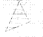
In Fig. 1, conceptually show view according to the parallel processing of pel level.
In Fig. 1, PM0 represents different pels to PMn-1, and PU0 represents processing unit to PUn-1, and MM0 represents memory module to MMn-1.
When the pel PM0 that will have identical relatively size offers processing unit PU0 to PUn-1 to PMn-1, processing unit PU0 to the load on the PUn-1 be balance and can carry out effective parallel processing.
The parallel processing of level according to pixels
This is the meticulousst parallel processing technique of a kind of granularity.
Fig. 2 shows based on the view in the parallel processing parallel processing technique on the pixel level, on the pel level conceptive.
As shown in Figure 2, in the parallel processing technique of level according to pixels, when diabolo carries out rasterisation, in the unit of the rectangular area that is called " element marking (pixe1stamp) PS " that form by the pixel of arranging in according to 2 * 8 matrixes, to produce pixel.
In the example of Fig. 2, eight element markings have altogether been generated from element marking PS0 to element marking PS7.Handle simultaneously to maximum 16 pixels among the PS7 being included in these element markings PS0.
According to the fine degree of granularity, aspect parallel processing, this technology is more effective than other technology.
But, carry out under the situation of parallel processing in the area dividing of utilizing of above explanation, in order to make processing unit parallel running effectively, need in advance the object that will draw in the zone to be classified, therefore, very heavy to the burden that scene data is analyzed.
In addition, after the performance in the scene data of a frame all occurs, do not begin to describe, when still the Immediate Mode that begins to describe according to what is called is described, can not realize parallel characteristics at once when providing object data.
In addition, carrying out according to the pel level under the situation of parallel processing, in the light of actual conditions, variation occurring to aspect PMn-1 big or small, therefore, processing unit PU0 difference occurred to the time that a pel among the PUn-1 is handled at the pel PM0 that forms object.When this species diversity became big, the zone that processing unit is described was also very inequality, and the position of data lost, and therefore, for instance, the DRAM that forms memory module produces a page error continually, and performance descends.
In addition, in the occasion of using this technology, cost high problem in addition interconnects.In general, be used for the hardware of graphics process,, a plurality of memory modules be used for memory interleaving in order to widen the bandwidth of storer.
At this moment, as shown in Figure 1, need all processing unit PU0 are connected to MMn with internal memory module MM0 to PUn-1.
On the other hand, carrying out according to pixel level under the situation of parallel processing, as mentioned above, the validity with parallel processing is according to the fine degree of the granularity better advantage that becomes.Comprise actual filtering owing to handle, therefore, handle according to program shown in Figure 3.
That is,, for example, calculate (ST1) to carrying out the needed various types of data deviations of rasterisation (Z, structure coordinate, color etc.) and other DDA parameter to DDA (digital differential analyser) parameter.
Then, reading out structure data (ST2) from storer, the antithetical phrase word is reallocated (ST3), then, by circuit in length and breadth the data overall situation is distributed to processing unit (ST4).
Then, carry out structure filtering (ST5).In this case, utilize the structured data read and when to (processing unit PU0 carries out four adjacent interpolations or other filtering to PU3 for u, the decimal fraction that obtains when v) calculate the address.
Then, carry out processing, specifically, the structured data after the filtering and the Various types of data after the rasterisation are used for operation (ST5) on pixel cell according to pixel level (by pixel operation).
In addition, in the frame buffer and Z impact damper of memory module MM0 to the MM3, be depicted in the process of handling according to pixel level pixel data by various types of tests.
Therefore mention in passing, the memory access of structure read-out system is different with the memory access of Grafmaster, need be subordinated to reading of data in the storer of another module.
Therefore, for the memory access of structure read-out system, need interconnection, as above-mentioned circuit in length and breadth.
But, as mentioned above, relevant image processing apparatus is distributed to processing unit with the data overall situation, carry out structure filtering then, therefore the data volume that has overall situation distribution is big (for example, 4Tbps), to be become aspect big or small big as the circuit in length and breadth of global bus and has hindered shortcomings such as processing speed raising from the viewpoint of interconnect delay.
Summary of the invention
An object of the present invention is to provide a kind of image processing apparatus and method thereof that can realize reducing the size of circuit in length and breadth and can realize improving processing speed.
To achieve these goals, a first aspect of the present invention be a kind of wherein by a plurality of processing module shared processing data to carry out the image processing apparatus of parallel processing, wherein: each in a plurality of processing modules all comprises: memory module is used for storing at least the data relevant with filtering; Treatment circuit is used for according to deal with data, obtains being used for the data of filtering, and by corresponding memory interleaving access, the designated treatment of being scheduled to; The first operational processes element is used for deal with data and the data after the filtering that described treatment circuit obtains according to appointment, and carries out operational processes according to pixel cell; And the second operational processes element, be used for carrying out filtering according to data that are used for filtering that obtain by described treatment circuit and the data relevant that are stored in described memory module with filtering, and receive operational processes data from the first operational processes element, to be painted into memory module through the data of operational processes then, in described a plurality of processing module each also comprises circuit in length and breadth, the global bus that is connected with a plurality of second operational processes elements as a plurality of first operational processes elements that are used for described processing module, the data that are used for filtering that will be obtained by the described treatment circuit in each processing module offer the second operational processes element in the same treatment module, the first operational processes element in the processing module corresponding will be offered from the data after the filtering of the second operational processes element in each processing module, and the second operational processes element will be offered from the operational processes data of the first operational processes element with this processing.
According to first aspect, the treatment circuit of each processing module comprises the device that is used to the time of regulating, and makes processing time of specific data become and equates with the time that the data after the filtering is offered the first operational processes element.
Second aspect of the present invention be a kind of wherein by a plurality of processing module shared processing data to carry out the image processing method of parallel processing, this method comprises: the data that obtain being used for filtering, and according to deal with data, by corresponding memory interleaving access, the designated treatment of being scheduled to; According to the data that are used for filtering and the data relevant that are stored in memory module that obtain, carry out filtering with filtering; By global bus, will in each processing module, the data after the filtering offer predetermined processing module; And according to the data after designated treatment data that obtain and the filtering, in pixel cell, carry out operational processes, and will be painted into described memory module, the data after in processing module, accepting filter through the data of operational processes.
Best, this method also comprises the step of regulating each processing module time, make processing time of specific data become with filtering is provided after time of data equate.
In addition, in the present invention, the processing that needs filtering is structure dependent processing.
In addition, above-mentioned parallel processing is the parallel processing of level according to pixels.
According to the present invention, for example, circuit is set vertex data is operated, pel is set, and the performance of the configuration information of specified structure is outputed to processing module.
According to from the information that circuit is set, the deviation of the treatment circuit calculated example of each processing module such as DDA parameter, especially Various types of data (Z, structure coordinate, color etc.) etc., and carry out needed other DDA parameter of rasterisation.
In addition, each treatment circuit judges according to supplemental characteristic whether triangle is the zone of its appointment, and, when being its appointed area, carry out rasterisation.
In addition, each treatment circuit calculates the MipMap level by calculating LOD, and calculates (u, the v) address computation that is used for structural reference.
Then, each treatment circuit outputs to the second operational processes element with structure coordinate that obtains and the address information that is used for structural reference etc.
On the other hand, each treatment circuit color except structure and out of Memory that will obtain offers the first operational processes element.
In addition, structure dependent coordinate data and the address date that provides from treatment circuit is provided the second operational processes element of each processing module, reading out structure data from memory module, and utilize the structured data of reading and calculating (u, v) the decimal fraction that obtains during the address is carried out four adjacent interpolations or other structure filtering.
By circuit in length and breadth, will offer from the structured data after the filtering of the second operational processes element for example have with the processing module that indicates corresponding frame buffer in the first operational processes element.
Carry out data after the structure filtering according to the data except structural information that provide from treatment circuit with by the second operational processes element by processing module that circuit in length and breadth receives, the first operational processes element of this processing module carries out the processing of level according to pixels and the result is outputed to the second operational processes element.
Then, the second operational processes element receives the result who handles according to pixel level who provides from the first operational processes element and the pixel data that will pass through various types of tests the process that according to pixels level is handled is painted in the memory module.
The above-mentioned processing of executed in parallel in module.
Description of drawings
Fig. 1 is the view that conceptually shows according to the parallel processing of pel level.
Fig. 2 be conceptually show based on the technology of parallel processing on pixel level, according to the view of the parallel processing of pel level.
Fig. 3 is the view that the handling procedure of the structure filtering that comprises the associated picture treating apparatus has been described.
Fig. 4 is the block scheme according to the configuration of the embodiment of image processing apparatus of the present invention.
Fig. 5 is the view according to the basic structure and the treatment scheme of the image processing apparatus of present embodiment.
Fig. 6 is the view according to the example of structure of the key component of the DDA circuit of present embodiment.
Fig. 7 is the view according to the object lesson of the structure of the circuit in length and breadth of present embodiment.
Fig. 8 is the view that has conceptually illustrated according to the processing of the image processing apparatus of present embodiment.
Fig. 9 is the view according to notional treatment scheme of the image processing apparatus of present embodiment.
Embodiment
Fig. 4 is the block scheme according to the configuration of an embodiment of image processing apparatus of the present invention.
As shown in Figure 4, have the circuit of setting 11, processing module 12-0 to 12-3 and circuit 13 in length and breadth according to the image processing apparatus 10 of present embodiment.
In this image processing apparatus 10, with a plurality of, be four in the present embodiment, processing module 12-0 is parallel-connected to 12-3 circuit 11 is set.A plurality of processing module 12-0 to 12-3 shared processing data to carry out parallel processing.
Yet, for the structure read-out system, need carry out memory access, but will be used for such visit as the circuit in length and breadth 13 of global access bus to other processing module.
Below, be described in proper order with reference to the 26S Proteasome Structure and Function of accompanying drawing parts.
Data transmission and processing module 12-0 that 11 couples of CPU of circuit and external memory storage are set control to the data transmission of 12-3, to the vertex data executable operations, a pel is set, and the specified structure performance of configuration information is outputed to processing module 12-0 to 12-3.
Specifically, when the input data, circuit 11 is set carries out by vertex operations.
In this processing procedure, when the vertex data of importing three-dimensional coordinate, normal vector and structure coordinate, to the vertex data executable operations.As representational operation, be useful on the operational processes of coordinate transform, as distortion, the operational processes that is used to throw light on of the object on the screen, projection etc. be used for the operational processes of montage.
Processing module 12-0 has DDA (digital differential analyser) circuit 121-0, the first operational processes element (operational processes element 1) 122-0, the second operational processes element (operational processes element 2) 123-0 as treatment circuit and memory module (MEM) 124-0 that is formed by for example DRAM.
Similarly, processing module 12-1 has DDA circuit 121-1, the first operational processes element (operational processes element 1) 122-1, the second operational processes element (operational processes element 2) 123-1 as treatment circuit and memory module (MEM) 124-1 that is formed by for example DRAM.
Processing module 12-2 has DDA circuit 121-2, the first operational processes element (operational processes element 1) 122-2, the second operational processes element (operational processes element 2) 123-2 as treatment circuit and memory module (MEM) 124-2 that is formed by for example DRAM.
Processing module 12-3 has DDA circuit 121-3, the first operational processes element (operational processes element 1) 122-3, the second operational processes element (operational processes element 2) 123-3 as treatment circuit and memory module (MEM) 124-3 that is made of for example DRAM.
In addition, as described in detail later on,, will interconnect to 123-3 to the 122-3 and the second operational processes element 123-0 to the first operational processes element 122-0 among the 12-3 at processing module 12-0 by circuit 13 in length and breadth.
Fig. 5 is according to the basic structure of the image processing apparatus of present embodiment and treatment scheme.Notice that in Fig. 5 the arrow with circle is represented structure dependent data stream, and does not have the arrow of circle to represent the data stream relevant with pixel.
In the present embodiment, in 12-3, memory module 124-0 interweaved to 124-3 is pre-sizing, for example 4 * 4 unit, rectangular area at processing module 12-0.
Specifically, as shown in Figure 5, so-called frame buffer is interweaved to all memory modules, and structure memory is dispersed in memory module 124-0 in 124-3.
According to from the information that circuit 11 is set, the DDA circuit 121-0 in processing module 12-0 calculates the DDA parameter.
In this processing procedure, deviation and other DDA parameter of carrying out the needed Various types of data of rasterisation (Z, structure coordinate, color etc.) are calculated.
In addition, according to supplemental characteristic, DDA circuit 121-0 for example judges triangle whether in the appointed area that this circuit is handled, and when in this zone, carries out rasterisation.
Specifically, it judges whether this triangle belongs to the zone that is assigned to it, and for example rasterisation when belonging to it, is carried out to Various types of data (Z, structure coordinate, color etc.) in the zone that is interweaved by unit, 4 * 4 pixel rectangular area.In this case, the unit that generated is 2 * 2 pixels each local each cycle of module.
Then, DDA circuit 121-0 proofreaies and correct the panorama of structure coordinate.This processing stage comprise by calculating LOD (level of detail, details level) and calculate (u, the v) address that MipMap level and calculating are used for structural reference.
For example, as shown in Figure 6, address information that DDA circuit 121-0 utilizes structural system DDA part 1211, be used for structural reference etc. is carried out the structure treatment about structure coordinate, and, structure dependent information is outputed to the second operational processes element 123-0 by the first operational processes element 122-0 and circuit 13 in length and breadth.
On the other hand, DDA circuit 121-0 utilizes another DDA part 1212 to carry out color and other processing except structure, and the result is outputed to the first operational processes element 122-0.
In the present embodiment, only be equipped with FIFO (first in first out) for each DDA circuit 121 (0 to 3), and each DDA circuit 121 (0 to 3) is according to adjusting time time that structural system is carried out filtering at the data input side of other DDA part 1212.
In addition, although other DDA part 1212 only generates by the storer specified part that interweaves,, structural system DDA part 1211 generates the structured data that is assigned to this structure for all pixels.
According to the data except structural information that provide from DDA circuit 121-0 and by circuit 13 in length and breadth receive by second operational processes element 123-0 the data to 123-3 carry out structure filtering after of processing module 12-0 to 12-3, the first operational processes element 122-0 carries out the processing (by pixel operation) according to pixel level and by circuit 13 in length and breadth the result is outputed to the second operational processes element 123-0.
In the process of handling according to pixel level, the structured data after the filtering is used for the operation relevant with pixel cell with rasterisation Various types of data afterwards.Here the processing of Zhi Hanging is handled corresponding with pixel level illumination (by pixel illumination) or other so-called pixel shadow memory.
Structure dependent coordinate data and the address date that provides from DDA circuit 121-0 is provided the second operational processes element 123-0, from memory module 124-0 reading out structure data, carry out structure filtering, and by circuit 13 in length and breadth with the structured data after the filtering output to have with the processing module that indicates corresponding frame buffer in the first operational processes element 122-0 any one in the 122-3.
In this case, utilize the structured data read and to (the second operational processes element 123-0 carries out four adjacent interpolations or other filtering for u, the decimal fraction that obtains when v) calculate the address.
In addition, the second operational processes element 123-0 result of the pixel level that provides from the first operational processes element 122-0 is provided and will be painted into memory module 124-0 by the pixel data by various tests the process of handling according to pixel level.
DDA circuit 121-1 in processing module 12-1 especially carries out deviation and other DDA parameter of the needed Various types of data of rasterisation (Z, structure coordinate, color etc.) according to from the information calculations DDA parameter that circuit 11 is set.
In addition, according to supplemental characteristic, DDA circuit 121-1 judges for example whether triangle is its appointed area, and when being the appointment zone, carries out rasterisation.
Specifically, it judges that whether this triangle is its appointed area, and for example, whether it belongs to the zone that interweaves in unit, 4 * 4 pixel rectangular area, when belonging to, carries out rasterisation to Various types of data (Z, structure coordinate, color etc.).In this case, the unit that generated is 2 * 2 pixels each local each cycle of module.
Then, DDA circuit 121-1 proofreaies and correct the skeleton view of structure coordinate.This processing procedure comprises by calculating LOD (details level) calculates (u, the v) address that MipMap level and calculating are used for structural reference.
For example, as shown in Figure 6, address information that DDA circuit 121-1 utilizes structural system DDA part 1211, be used for structural reference etc. is carried out the structure treatment about structure coordinate, and, structure dependent information is outputed to the second operational processes element 123-1 by the first operational processes element 122-1 and circuit 13 in length and breadth.
On the other hand, DDA circuit 121-1 utilizes another DDA part 1212 to carry out color and other processing except structure, and the result is outputed to the first operational processes element 122-1.
According to the data except structural information that provide from DDA circuit 121-1 and by circuit 13 in length and breadth receive by second operational processes element 123-0 the data to 123-3 carry out structure filtering after of processing module 12-0 to 12-3, the first operational processes element 122-1 carries out the processing of level according to pixels (by pixel operation) and by circuit 13 in length and breadth the result is outputed to the second operational processes element 123-1.
In the process that according to pixels level is handled, the structured data after the filtering is used for the operation relevant with pixel cell with rasterisation Various types of data afterwards.Here the processing of Zhi Hanging is handled corresponding with pixel level illumination or other so-called pixel shadow memory.
Structure dependent coordinate data and the address date that provides from DDA circuit 121-1 is provided the second operational processes element 123-1, from memory module 124-1 reading out structure data, carry out structure filtering, and by circuit 13 in length and breadth with the structured data after the filtering output to have with the processing module that indicates corresponding frame buffer in the first operational processes element 122-0 any one in the 122-3.
In this case, utilize the structured data read and to (the second operational processes element 123-1 carries out four adjacent interpolations or other filtering for u, the decimal fraction that obtains when v) calculate the address.
In addition, the second operational processes element 123-1 result of the pixel level that provides from the first operational processes element 122-1 is provided and will be painted among the memory module 124-1 by the pixel data by various tests the process of handling according to pixel level.
DDA circuit 121-2 in processing module 12-2 especially carries out deviation or other DDA parameter of the needed Various types of data of rasterisation (Z, structure coordinate, color etc.) according to from the information calculations DDA parameter that circuit 11 is set.
In addition, according to supplemental characteristic, DDA circuit 121-2 judges for example whether triangle is its appointed area, and when being the appointment zone, carries out rasterisation.
Specifically, it judges that whether this triangle is its appointed area, and for example, whether it belongs to the zone that interweaves in unit, 4 * 4 pixel rectangular area, when belonging to, carries out rasterisation to Various types of data (Z, structure coordinate, color etc.).In this case, the unit that generated is 2 * 2 pixels each local each cycle of module.
Then, DDA circuit 121-2 proofreaies and correct the skeleton view of structure coordinate.This processing procedure comprises by calculating LOD (details level) calculates (u, the v) address that MipMap level and calculating are used for structural reference.
For example, as shown in Figure 6, address information that DDA circuit 121-2 utilizes structural system DDA part 1211, be used for structural reference etc. is carried out the structure treatment about structure coordinate, and, structure dependent information is outputed to the second operational processes element 123-2 by the first operational processes element 122-2 and circuit 13 in length and breadth.
On the other hand, DDA circuit 121-2 utilizes another DDA part 1212 to carry out color and other processing except structure, and the result is outputed to the first operational processes element 122-2.
According to the data except structural information that provide from DDA circuit 121-2 and by circuit 13 in length and breadth receive by second operational processes element 123-0 the data to 123-3 carry out structure filtering after of processing module 12-0 to 12-3, the first operational processes element 122-2 carries out the processing of level according to pixels (by pixel operation) and by circuit 13 in length and breadth the result is outputed to the second operational processes element 123-2.
In the process that according to pixels level is handled, the structured data after the filtering is used for the operation relevant with pixel cell with rasterisation Various types of data afterwards.Here the processing of Zhi Hanging is handled corresponding with pixel level illumination or other so-called pixel shadow memory.
Structure dependent coordinate data and the address date that provides from DDA circuit 121-2 is provided the second operational processes element 123-2, from memory module 124-2 reading out structure data, carry out structure filtering, and by circuit 13 in length and breadth with the structured data after the filtering output to have with the processing module that indicates corresponding frame buffer in the first operational processes element 122-0 any one in the 122-3.
In this case, utilize the structured data read and to (the second operational processes element 123-2 carries out four adjacent interpolations or other filtering for u, the decimal fraction that obtains when v) calculate the address.
In addition, the second operational processes element 123-2 result of the pixel level that provides from the first operational processes element 122-2 is provided and will be painted into memory module 124-2 by the pixel data by various tests the process of handling according to pixel level.
DDA circuit 121-3 in processing module 12-3 especially carries out deviation or other DDA parameter of the needed Various types of data of rasterisation (Z, structure coordinate, color etc.) according to from the information calculations DDA parameter that circuit 11 is set.
In addition, according to supplemental characteristic, DDA circuit 121-3 judges for example whether triangle is its appointed area, and when being the appointment zone, carries out rasterisation.
Specifically, it judges that whether this triangle is its appointed area, and for example, whether it belongs to the zone that interweaves in unit, 4 * 4 pixel rectangular area, when belonging to, carries out rasterisation to Various types of data (Z, structure coordinate, color etc.).In this case, the unit that generated is 2 * 2 pixels each local each cycle of module.
Then, DDA circuit 121-3 proofreaies and correct the skeleton view of structure coordinate.This processing procedure comprises by calculating LOD (details level) calculates (u, the v) address that MipMap level and calculating are used for structural reference.
For example, as shown in Figure 6, address information that DDA circuit 121-3 utilizes structural system DDA part 1211, be used for structural reference etc. is carried out the structure treatment about structure coordinate, and, structure dependent information is outputed to the second operational processes element 123-3 by the first operational processes element 122-3 and circuit 13 in length and breadth.
On the other hand, DDA circuit 121-3 utilizes another DDA part 1212 to carry out color and other processing except structure, and the result is outputed to the first operational processes element 122-3.
According to the data except structural information that provide from DDA circuit 121-3 and by circuit 13 in length and breadth receive by second operational processes element 123-0 the data to 123-3 carry out structure filtering after of processing module 12-0 to 12-3, the first operational processes element 122-3 carries out the processing of level according to pixels (by pixel operation) and by circuit 13 in length and breadth the result is outputed to the second operational processes element 123-3.
In the process that according to pixels level is handled, the structured data after the filtering is used for the operation relevant with pixel cell with rasterisation Various types of data afterwards.Here the processing of Zhi Hanging is handled corresponding with pixel level illumination or other so-called pixel shadow memory.
Structure dependent coordinate data and the address date that provides from DDA circuit 121-3 is provided the second operational processes element 123-3, from memory module 124-3 reading out structure data, carry out structure filtering, and by circuit 13 in length and breadth with the structured data after the filtering output to have with the processing module that indicates corresponding frame buffer in the first operational processes element 122-0 any one in the 122-3.
In this case, utilize the structured data read and to (the second operational processes element 123-3 carries out four adjacent interpolations or other filtering for u, the decimal fraction that obtains when v) calculate the address.
In addition, the second operational processes element 123-3 result of the pixel level that provides from the first operational processes element 122-3 is provided and will be painted into memory module 124-3 by the pixel data by various tests the process of handling according to pixel level.
Fig. 7 is the view according to the object lesson of the structure of the system of global bus in the circuit in length and breadth of present embodiment.
As shown in Figure 7, circuit 13 has four groups of interconnected set GRP0 of first to the 4th to GRP3 in length and breadth, and four structure lines constitute one group.
The first interconnected set GRP0 has four interconnection tex00 to tex03, the second interconnected set GRP1 has four interconnection tex10 to tex13, the 3rd interconnected set GRP2 has four interconnection tex20 to tex23, and the 4th interconnected set GRP3 has four interconnection tex30 to tex33.
In addition, the terminal of the second operational processes element 123-0 that will be in processing module 12-0 is connected to interconnection tex00, the interconnection tex10 among the second interconnected set GRP1, the interconnection tex20 among the 3rd interconnected set GRP2 and the interconnection tex30 in the 4th interconnected set GRP3 among the first interconnected set GRP0.
In the same way, the terminal of the second operational processes element 123-1 that will be in processing module 12-1 is connected to interconnection t ex01, the interconnection tex11 among the second interconnected set GRP1, the interconnection tex21 among the 3rd interconnected set GRP2 and the interconnection tex31 among the 4th interconnected set GRP3 among the first interconnected set GRP0.
The terminal of the second operational processes element 123-2 that will be in processing module 12-2 is connected to interconnection tex02, the interconnection tex12 among the second interconnected set GRP1, the interconnection tex22 among the 3rd interconnected set GRP2 and the interconnection tex32 among the 4th interconnected set GRP3 among the first interconnected set GRP0.
The terminal of the second operational processes element 123-3 that will be in processing module 12-3 is connected to interconnection tex03, the interconnection tex13 among the second interconnected set GRP1, the interconnection tex23 among the 3rd interconnected set GRP2 and the interconnection tex33 among the 4th interconnected set GRP3 among the first interconnected set GRP0.
Four among first interconnected set GRP0 interconnection tex00-tex03 are connected to the terminal of the first operational processes element 122-0 among the processing module 12-0.
In the same way, four among second interconnected set GRP1 interconnection tex10-tex13 are connected to the terminal of the first operational processes element 122-1 among the processing module 12-1.
Four among the 3rd interconnected set GRP2 interconnection tex20-tex23 are connected to the terminal of the first operational processes element 122-2 among the processing module 12-2.
Four among the 4th interconnected set GRP3 interconnection tex30-tex33 are connected to the terminal of the first operational processes element 122-3 among the processing module 12-3.
In image processing apparatus 10, carry out processing as Fig. 8 conceptually illustrated with this structure.
That is, in module, will give structure DDA part 1211 and other structure DDA part 1212 from the data allocations that circuit 11 is set.According to structural information of coming self-structure DDA part 1211 and the structured data in storer 124 (by the data stream of (1) expression), carry out structure filtering by the second operational processes element 123.
By circuit 13 in length and breadth the structured data after the filtering is distributed to the first operational processes element 122 (by the data stream of (2) expression) in the module of request.
Then, in the first operational processes element 122, carry out the processing of level according to pixels, and the result is sent to the second operational processes element 123, thus these data are painted into memory module 124 (by the data stream of (3) expression) by circuit 13 in length and breadth.
Below, with reference to Fig. 5 the operation of being undertaken by the structure of above Fig. 4 is described.
At first, 11 pairs of vertex datas of circuit are set operate, pel is set, and the structural behaviour of the appointment of configuration information is outputed to processing module 12-0 to 12-3.
According to from the information that circuit 11 is set, calculate DDA parameter to the DDA circuit 121-0 among the 12-3 to 121-3 at processing module 12-0, especially carry out deviation or other DDA parameter of the needed Various types of data of rasterisation (Z, structure coordinate, color etc.).
According to supplemental characteristic, DDA circuit 121-0 judges to 121-3 for example whether triangle is its appointed area, and when being its appointed area, carries out rasterisation.
In addition, DDA circuit 121-0 calculates (u, the v) address that mipmap level and calculating are used for structural reference to 121-3 by calculating LOD.
Then, to 122-3 and circuit 13 in length and breadth, structure coordinate that DDA circuit 121-0 will be obtained by structural system DDA part 1211 to 121-3 and the address information that is used for structural reference etc. output to the second operational processes element 123-0 to 123-3 by the first operational processes element 122-0.
On the other hand, DDA circuit 121-0 offers the first operational processes element 122-0 to 122-3 to 121-3 with color and the out of Memory except structure that obtained by other DDA part 1212.
Receive the coordinate data and the address date of the relevant structure that provides from DDA circuit 121-0 to 121-3 to 123-3 at the second operational processes element 123-0 of processing module 12-0 in the 12-3, reading out structure data from memory module 124-0 to 124-3, utilize the structured data read then and (u, v) the decimal fraction that obtains of address is carried out four adjacent interpolations or other structure filtering by calculating.
By circuit 13 in length and breadth, will offer for example first operational processes element 122-1 in processing module 12-1 from the structured data of the second operational processes element 123-0 after the filtering of 123-3 with frame buffer corresponding with sign.
According to the data except structural information that provide from DDA circuit 121-1 and by circuit 13 in length and breadth receive by second operational processes element 123-0 the data to 123-3 carry out structure filtering after of processing module 12-0 to 12-3, the first operational processes element 122-1 in processing module 12-1 carries out and outputs to the second operational processes element 123-1 according to the processing of pixel level and with the result.
Then, the result provided by the first operational processes element 122-1, handle according to pixel level is provided the second operational processes element 123-1, and the pixel data that will pass through various tests in the process of handling according to pixel level is painted into memory module 124-1.
The above-mentioned processing of executed in parallel on this module.
As mentioned above, as shown in Figure 9, present embodiment is carried out DDA and is handled (ST11), read structured data (ST12) from storer then, carry out sub-word reallocation and handle (ST13), carry out structure filtering (ST14) then, by circuit 13 in length and breadth the data overall situation is distributed to the first operational processes element (ST15) of each processing module then, carry out the processing on the level according to pixels then, specifically, utilize filtering structured data and rasterisation Various types of data afterwards afterwards, according to pixels the unit is operated, and will in the process of handling according to pixel level, be painted into the frame buffer (ST16) of memory module, can show following effect thus by the pixel data of each class testing.
That is,, therefore, can make circuit in length and breadth 13 reduce size as global bus owing to make the data minimizing by filtering after, again data are distributed.
In addition, owing to can make filtering traffic localization before, make the path localization that needs wider bandwidth from memory module to the second operational processes element, and therefore can realize higher processing speed.
Therefore, has the advantage that can realize design easily and can reduce the image processing apparatus of interconnection cost and interconnect delay.
Industrial usability
As mentioned above, when a plurality for the treatment of apparatus shared processing data when carrying out parallel processing, according to this Bright image processing apparatus and method thereof can reduce the quantity of the in length and breadth interconnection of circuit and make the chi of circuit Very little reducing. Therefore, easily design and can reduce the interconnection cost and interconnection postpones, therefore, can Apply the present invention to figure LSI etc.
Claims (9)
1. image processing apparatus, wherein a plurality of processing module shared processing data, to carry out parallel processing, wherein:
In described a plurality of processing module each all comprises:
Memory module is used for storing at least the data relevant with filtering;
Treatment circuit is used to obtain being used for the data of filtering and according to deal with data, by the storer interpolation of correspondence, carries out the designated treatment of decision in advance;
The first operational processes element is used for according to the deal with data of appointment and data that obtain at described treatment circuit, after the filtering, and according to pixels the unit carries out operational processes;
The second operational processes element, be used for carrying out filtering according to data that are used for filtering that obtain by described treatment circuit and the data relevant that are stored in described memory module with filtering, and receive operational processes data from the described first operational processes element, to deliver to this memory module through the data of operational processes then, and
Circuit in length and breadth, it is as being used to connect a plurality of first operational processes elements of described processing module and the global bus of a plurality of second operational processes elements, the data that are used for filtering that will be obtained by the described treatment circuit in each processing module offer the second operational processes element in the same treatment module, will be from the second operational processes element in each processing module, data after the filtering offer with this and handle the first operational processes element in the corresponding processing module, and will offer the second operational processes element from the operational processes data of the first operational processes element.
2. image processing apparatus according to claim 1, wherein the treatment circuit of each processing module all comprises and is used for the adjusting time, makes the device that processing time of specific data becomes and equates with the time that the data after the filtering is offered the first operational processes element.
3. image processing apparatus according to claim 1 also comprises circuit is set, and is used to carry out the operation about the vertex data of pel, a pel is set, and specific data is outputed to the treatment circuit of processing module.
4. image processing apparatus according to claim 1, the processing that wherein needs filtering are structure dependent processing.
5. image processing apparatus according to claim 1, wherein, described parallel processing is the parallel processing of level according to pixels.
6. image processing method, wherein a plurality of processing module shared processing data, so that carry out parallel processing, this method comprises the steps:
Acquisition is used for the data of filtering, and is used for the deal with data according to each processing module, by corresponding memory interleaving access, and the designated treatment that is predetermined;
Carry out filtering according to data that are used for filtering that obtain and the data relevant that are stored in memory module with filtering;
By global bus, the data after the filtering in each processing module are offered predetermined processing module; And
According to the data after designated treatment data that obtain and the filtering, according to pixels the unit executable operations is handled and will be arrived described memory module through the data description of operational processes, the data after accepting filter in processing module.
7. image processing method according to claim 6 also comprises the steps: to regulate each processing module time, make processing time of specific data become with filtering is provided after time of data equate.
8. image processing method according to claim 6, the processing that wherein needs filtering are structure dependent processing.
9. image processing method according to claim 6, wherein said parallel processing are the parallel processings of level according to pixels.
Applications Claiming Priority (2)
| Application Number | Priority Date | Filing Date | Title |
|---|---|---|---|
| JP2001379349A JP3838086B2 (en) | 2001-12-12 | 2001-12-12 | Image processing apparatus and method |
| JP379349/2001 | 2001-12-12 |
Publications (2)
| Publication Number | Publication Date |
|---|---|
| CN1491402A CN1491402A (en) | 2004-04-21 |
| CN1282128C true CN1282128C (en) | 2006-10-25 |
Family
ID=19186757
Family Applications (1)
| Application Number | Title | Priority Date | Filing Date |
|---|---|---|---|
| CNB02804889XA Expired - Fee Related CN1282128C (en) | 2001-12-12 | 2002-12-11 | Image processing device and method |
Country Status (6)
| Country | Link |
|---|---|
| US (1) | US7437021B2 (en) |
| EP (1) | EP1460582A4 (en) |
| JP (1) | JP3838086B2 (en) |
| KR (1) | KR100929746B1 (en) |
| CN (1) | CN1282128C (en) |
| WO (1) | WO2003054800A1 (en) |
Families Citing this family (18)
| Publication number | Priority date | Publication date | Assignee | Title |
|---|---|---|---|---|
| US7079148B2 (en) * | 2003-07-23 | 2006-07-18 | Hewlett-Packard Development Company, L.P. | Non-volatile memory parallel processor |
| US8775112B2 (en) | 2003-09-15 | 2014-07-08 | Nvidia Corporation | System and method for increasing die yield |
| US8732644B1 (en) | 2003-09-15 | 2014-05-20 | Nvidia Corporation | Micro electro mechanical switch system and method for testing and configuring semiconductor functional circuits |
| US8775997B2 (en) | 2003-09-15 | 2014-07-08 | Nvidia Corporation | System and method for testing and configuring semiconductor functional circuits |
| US8711161B1 (en) | 2003-12-18 | 2014-04-29 | Nvidia Corporation | Functional component compensation reconfiguration system and method |
| JP2005234727A (en) * | 2004-02-18 | 2005-09-02 | Toshiba Corp | Device, system and method for processing image |
| US7091982B2 (en) * | 2004-05-14 | 2006-08-15 | Nvidia Corporation | Low power programmable processor |
| KR100868396B1 (en) * | 2004-08-26 | 2008-11-11 | 인텔 코오퍼레이션 | Graphic processing system and method for subdividing geometry images |
| US8723231B1 (en) | 2004-09-15 | 2014-05-13 | Nvidia Corporation | Semiconductor die micro electro-mechanical switch management system and method |
| US8711156B1 (en) | 2004-09-30 | 2014-04-29 | Nvidia Corporation | Method and system for remapping processing elements in a pipeline of a graphics processing unit |
| JP2006202211A (en) * | 2005-01-24 | 2006-08-03 | Fujitsu Ltd | Image drawing device and image drawing method |
| JP4637640B2 (en) * | 2005-05-16 | 2011-02-23 | 三菱電機株式会社 | Graphic drawing device |
| US8228328B1 (en) | 2006-11-03 | 2012-07-24 | Nvidia Corporation | Early Z testing for multiple render targets |
| US8724483B2 (en) | 2007-10-22 | 2014-05-13 | Nvidia Corporation | Loopback configuration for bi-directional interfaces |
| US9331869B2 (en) | 2010-03-04 | 2016-05-03 | Nvidia Corporation | Input/output request packet handling techniques by a device specific kernel mode driver |
| US9304731B2 (en) * | 2011-12-21 | 2016-04-05 | Intel Corporation | Techniques for rate governing of a display data stream |
| JP5993267B2 (en) * | 2012-10-04 | 2016-09-14 | オリンパス株式会社 | Image processing device |
| JP6335335B2 (en) * | 2014-06-30 | 2018-05-30 | インテル・コーポレーション | Adaptive partition mechanism with arbitrary tile shapes for tile-based rendering GPU architecture |
Family Cites Families (17)
| Publication number | Priority date | Publication date | Assignee | Title |
|---|---|---|---|---|
| JPH0348979A (en) | 1989-07-17 | 1991-03-01 | Nec Corp | Parallel image processor |
| JP2858602B2 (en) | 1991-09-20 | 1999-02-17 | 三菱重工業株式会社 | Pipeline operation circuit |
| US5359674A (en) * | 1991-12-11 | 1994-10-25 | David Sarnoff Research Center, Inc. | Pyramid processor integrated circuit |
| JP2642039B2 (en) * | 1992-05-22 | 1997-08-20 | インターナショナル・ビジネス・マシーンズ・コーポレイション | Array processor |
| US5566284A (en) * | 1993-12-22 | 1996-10-15 | Matsushita Electric Industrial Co., Ltd. | Apparatus and method for mip-map generation using low-pass filtering based on resolution ratio |
| US5493643A (en) * | 1994-05-03 | 1996-02-20 | Loral Aerospace Corp. | Image generator architecture employing tri-level fixed interleave processing and distribution buses |
| JPH08335273A (en) | 1995-06-08 | 1996-12-17 | Hitachi Denshi Ltd | Image generating device |
| US5956744A (en) * | 1995-09-08 | 1999-09-21 | Texas Instruments Incorporated | Memory configuration cache with multilevel hierarchy least recently used cache entry replacement |
| US5638533A (en) * | 1995-10-12 | 1997-06-10 | Lsi Logic Corporation | Method and apparatus for providing data to a parallel processing array |
| JP3645024B2 (en) * | 1996-02-06 | 2005-05-11 | 株式会社ソニー・コンピュータエンタテインメント | Drawing apparatus and drawing method |
| US6104842A (en) * | 1996-06-10 | 2000-08-15 | Integrated Device Technology, Inc. | Geometry processing of digital video models and images |
| US6236405B1 (en) * | 1996-07-01 | 2001-05-22 | S3 Graphics Co., Ltd. | System and method for mapping textures onto surfaces of computer-generated objects |
| EP0825550A3 (en) | 1996-07-31 | 1999-11-10 | Texas Instruments Incorporated | Printing system and method using multiple processors |
| US6130967A (en) * | 1997-07-03 | 2000-10-10 | Tri Path Imaging, Inc. | Method and apparatus for a reduced instruction set architecture for multidimensional image processing |
| US6452603B1 (en) * | 1998-12-23 | 2002-09-17 | Nvidia Us Investment Company | Circuit and method for trilinear filtering using texels from only one level of detail |
| US6661424B1 (en) * | 2000-07-07 | 2003-12-09 | Hewlett-Packard Development Company, L.P. | Anti-aliasing in a computer graphics system using a texture mapping subsystem to down-sample super-sampled images |
| US6763150B1 (en) * | 2000-08-29 | 2004-07-13 | Freescale Semiconductor, Inc. | Image processing system with multiple processing units |
-
2001
- 2001-12-12 JP JP2001379349A patent/JP3838086B2/en not_active Expired - Fee Related
-
2002
- 2002-12-11 WO PCT/JP2002/012966 patent/WO2003054800A1/en active Application Filing
- 2002-12-11 CN CNB02804889XA patent/CN1282128C/en not_active Expired - Fee Related
- 2002-12-11 US US10/467,543 patent/US7437021B2/en not_active Expired - Fee Related
- 2002-12-11 KR KR1020037010540A patent/KR100929746B1/en not_active IP Right Cessation
- 2002-12-11 EP EP02788790A patent/EP1460582A4/en not_active Withdrawn
Also Published As
| Publication number | Publication date |
|---|---|
| EP1460582A4 (en) | 2008-11-19 |
| US20040196290A1 (en) | 2004-10-07 |
| EP1460582A1 (en) | 2004-09-22 |
| WO2003054800A1 (en) | 2003-07-03 |
| JP3838086B2 (en) | 2006-10-25 |
| JP2003178293A (en) | 2003-06-27 |
| US7437021B2 (en) | 2008-10-14 |
| KR100929746B1 (en) | 2009-12-03 |
| KR20040073280A (en) | 2004-08-19 |
| CN1491402A (en) | 2004-04-21 |
Similar Documents
| Publication | Publication Date | Title |
|---|---|---|
| CN1282128C (en) | Image processing device and method | |
| CN1258154C (en) | Multiprocessor system, data processing system, data processing method, and computer program | |
| CN1317682C (en) | System and method of optimizing graphics processing | |
| CN1288603C (en) | Image processing device and its assembly and rendering method | |
| CN1252648C (en) | Three-D graphics rendering apparatus and method | |
| CN100351896C (en) | Controller/driver for driving display panel | |
| CN1969299A (en) | Video generation device and video generation method | |
| CN1684104A (en) | Method and device for compressing and decompressing instrument in computer system | |
| CN1099655C (en) | Apparatus and method for drawing | |
| CN101046888A (en) | Rendering apparatus and method, and shape data generation apparatus and method | |
| CN101057261A (en) | Processing of 3-dimensional graphics | |
| CN1892636A (en) | Systems and methods of providing indexed load and store operations in a dual-mode computer processing environment | |
| CN1893564A (en) | Image special effect device, graphic processor and recording medium | |
| CN1711559A (en) | Characteristic region extraction device, characteristic region extraction method, and characteristic region extraction program | |
| CN1560797A (en) | 3-D image processing mechanism for reducing Z buffer zone flow rate | |
| CN1801219A (en) | Textrue filter of enhancing multi-mode filter capability employing parallel processing | |
| CN1536531A (en) | Image processing device and image processing method and processing program | |
| CN1942901A (en) | Image processing device and image processing method | |
| CN1846223A (en) | Method for optimization of an order for component mounting and apparatus for optimization of an order for component mounting | |
| CN1294539C (en) | Triangle polygon plotting device and triangle polygon plotting method | |
| CN101038664A (en) | Image processing apparatus and image processing method | |
| CN1652155A (en) | Method and apparatus for changing digital image size | |
| JP5552956B2 (en) | Image processing apparatus, image processing method, and program | |
| CN1886758A (en) | Method and apparatus for downscaling a digital matrix image | |
| CN101038676A (en) | Image processing apparatus and image processing method |
Legal Events
| Date | Code | Title | Description |
|---|---|---|---|
| C06 | Publication | ||
| PB01 | Publication | ||
| C10 | Entry into substantive examination | ||
| SE01 | Entry into force of request for substantive examination | ||
| C14 | Grant of patent or utility model | ||
| GR01 | Patent grant | ||
| C17 | Cessation of patent right | ||
| CF01 | Termination of patent right due to non-payment of annual fee |
Granted publication date: 20061025 Termination date: 20111211 |