CN1279377C - Photon crystal making method and optical device using same - Google Patents
Photon crystal making method and optical device using same Download PDFInfo
- Publication number
- CN1279377C CN1279377C CNB011219726A CN01121972A CN1279377C CN 1279377 C CN1279377 C CN 1279377C CN B011219726 A CNB011219726 A CN B011219726A CN 01121972 A CN01121972 A CN 01121972A CN 1279377 C CN1279377 C CN 1279377C
- Authority
- CN
- China
- Prior art keywords
- optical
- optical fiber
- face
- crystal
- light
- Prior art date
- Legal status (The legal status is an assumption and is not a legal conclusion. Google has not performed a legal analysis and makes no representation as to the accuracy of the status listed.)
- Expired - Fee Related
Links
- 0 C*1C*CCC1 Chemical compound C*1C*CCC1 0.000 description 1
Images


Classifications
-
- G—PHYSICS
- G02—OPTICS
- G02B—OPTICAL ELEMENTS, SYSTEMS OR APPARATUS
- G02B6/00—Light guides; Structural details of arrangements comprising light guides and other optical elements, e.g. couplings
- G02B6/02—Optical fibres with cladding with or without a coating
- G02B6/02295—Microstructured optical fibre
- G02B6/02309—Structures extending perpendicularly or at a large angle to the longitudinal axis of the fibre, e.g. photonic band gap along fibre axis
-
- B—PERFORMING OPERATIONS; TRANSPORTING
- B82—NANOTECHNOLOGY
- B82Y—SPECIFIC USES OR APPLICATIONS OF NANOSTRUCTURES; MEASUREMENT OR ANALYSIS OF NANOSTRUCTURES; MANUFACTURE OR TREATMENT OF NANOSTRUCTURES
- B82Y20/00—Nanooptics, e.g. quantum optics or photonic crystals
-
- G—PHYSICS
- G02—OPTICS
- G02F—OPTICAL DEVICES OR ARRANGEMENTS FOR THE CONTROL OF LIGHT BY MODIFICATION OF THE OPTICAL PROPERTIES OF THE MEDIA OF THE ELEMENTS INVOLVED THEREIN; NON-LINEAR OPTICS; FREQUENCY-CHANGING OF LIGHT; OPTICAL LOGIC ELEMENTS; OPTICAL ANALOGUE/DIGITAL CONVERTERS
- G02F1/00—Devices or arrangements for the control of the intensity, colour, phase, polarisation or direction of light arriving from an independent light source, e.g. switching, gating or modulating; Non-linear optics
- G02F1/01—Devices or arrangements for the control of the intensity, colour, phase, polarisation or direction of light arriving from an independent light source, e.g. switching, gating or modulating; Non-linear optics for the control of the intensity, phase, polarisation or colour
- G02F1/09—Devices or arrangements for the control of the intensity, colour, phase, polarisation or direction of light arriving from an independent light source, e.g. switching, gating or modulating; Non-linear optics for the control of the intensity, phase, polarisation or colour based on magneto-optical elements, e.g. exhibiting Faraday effect
- G02F1/095—Devices or arrangements for the control of the intensity, colour, phase, polarisation or direction of light arriving from an independent light source, e.g. switching, gating or modulating; Non-linear optics for the control of the intensity, phase, polarisation or colour based on magneto-optical elements, e.g. exhibiting Faraday effect in an optical waveguide structure
- G02F1/0955—Devices or arrangements for the control of the intensity, colour, phase, polarisation or direction of light arriving from an independent light source, e.g. switching, gating or modulating; Non-linear optics for the control of the intensity, phase, polarisation or colour based on magneto-optical elements, e.g. exhibiting Faraday effect in an optical waveguide structure used as non-reciprocal devices, e.g. optical isolators, circulators
-
- C—CHEMISTRY; METALLURGY
- C03—GLASS; MINERAL OR SLAG WOOL
- C03B—MANUFACTURE, SHAPING, OR SUPPLEMENTARY PROCESSES
- C03B2203/00—Fibre product details, e.g. structure, shape
- C03B2203/42—Photonic crystal fibres, e.g. fibres using the photonic bandgap PBG effect, microstructured or holey optical fibres
-
- G—PHYSICS
- G02—OPTICS
- G02B—OPTICAL ELEMENTS, SYSTEMS OR APPARATUS
- G02B6/00—Light guides; Structural details of arrangements comprising light guides and other optical elements, e.g. couplings
- G02B6/02—Optical fibres with cladding with or without a coating
- G02B6/02295—Microstructured optical fibre
- G02B6/02314—Plurality of longitudinal structures extending along optical fibre axis, e.g. holes
- G02B6/02319—Plurality of longitudinal structures extending along optical fibre axis, e.g. holes characterised by core or core-cladding interface features
- G02B6/02338—Structured core, e.g. core contains more than one material, non-constant refractive index distribution in core, asymmetric or non-circular elements in core unit, multiple cores, insertions between core and clad
-
- G—PHYSICS
- G02—OPTICS
- G02B—OPTICAL ELEMENTS, SYSTEMS OR APPARATUS
- G02B6/00—Light guides; Structural details of arrangements comprising light guides and other optical elements, e.g. couplings
- G02B6/02—Optical fibres with cladding with or without a coating
- G02B6/02295—Microstructured optical fibre
- G02B6/02314—Plurality of longitudinal structures extending along optical fibre axis, e.g. holes
- G02B6/0239—Comprising means for varying the guiding properties, e.g. tuning means
-
- G—PHYSICS
- G02—OPTICS
- G02F—OPTICAL DEVICES OR ARRANGEMENTS FOR THE CONTROL OF LIGHT BY MODIFICATION OF THE OPTICAL PROPERTIES OF THE MEDIA OF THE ELEMENTS INVOLVED THEREIN; NON-LINEAR OPTICS; FREQUENCY-CHANGING OF LIGHT; OPTICAL LOGIC ELEMENTS; OPTICAL ANALOGUE/DIGITAL CONVERTERS
- G02F2202/00—Materials and properties
- G02F2202/32—Photonic crystals
-
- Y—GENERAL TAGGING OF NEW TECHNOLOGICAL DEVELOPMENTS; GENERAL TAGGING OF CROSS-SECTIONAL TECHNOLOGIES SPANNING OVER SEVERAL SECTIONS OF THE IPC; TECHNICAL SUBJECTS COVERED BY FORMER USPC CROSS-REFERENCE ART COLLECTIONS [XRACs] AND DIGESTS
- Y02—TECHNOLOGIES OR APPLICATIONS FOR MITIGATION OR ADAPTATION AGAINST CLIMATE CHANGE
- Y02P—CLIMATE CHANGE MITIGATION TECHNOLOGIES IN THE PRODUCTION OR PROCESSING OF GOODS
- Y02P40/00—Technologies relating to the processing of minerals
- Y02P40/50—Glass production, e.g. reusing waste heat during processing or shaping
- Y02P40/57—Improving the yield, e-g- reduction of reject rates
Abstract
An optical device includes, in a predetermined section of an optical fiber, a first functional part having a plurality of Faraday crystal columns that are parallel to each other and almost penetrating perpendicularly to an optical axis of an optical fiber through a core thereof, and a second functional part having a plurality of holes that are parallel to each other and almost penetrating perpendicularly to the optical axis of the optical fiber 1 through the core thereof. A longitudinal direction of the Faraday crystal columns and a longitudinal direction of the holes form an angle of 45 degrees along a plane perpendicular to the optical axis. Thus, the optical device can be realized only by processing the optical fiber.
Description
The present invention relates to the various optical devices that optical communication etc. is used, particularly the voltage of the dispersion compensator of fiber optic wavelength and polarized wave, optoisolator, photomodulator, detection power transmission line and distribution wire etc. or electric current and the optical devices such as optical sensor that use.
Various optical devices in the past at first are described below.Optical device in the past shown in Figure 31 is the structural representation of optoisolator.This optoisolator has the 1st and the 2nd lens 1003 and 1004 that the optical system between the 1st optical fiber 1001 and the 2nd optical fiber 1002 is coupled, and has the polarizer (mirror) 005 between them, faraday element 1006 and analyzer (mirror) 1007.In addition, in Figure 31, the light beam 1009 in the optical system, its extension is represented with straight line.Have again, have in this optoisolator in order to make faraday element 1006 saturated and have enough magnetic field 1008.In addition, the polarizer 1005 constitutes 45 angles of spending mutually with analyzer 1007.Use garnet crystals etc. are as faraday crystal 1006.
The following describes the principle of optoisolator.In this optoisolator shown in Figure 31,, at first utilize the polarizer 1005 to be transformed to linearly polarized light by 1003 couplings of the 1st lens by the no polarized light that the 1st optical fiber 1001 takes place.Then, this linearly polarized light utilizes faraday element 1006, its plane of polarization rotation 45 degree.Plane of polarization has rotated the linearly polarized light of 45 degree, utilizes the analyzer 1007 that constitutes above-mentioned angle, all by the 2nd lens 1004 and 1002 couplings of the 2nd optical fiber.
On the other hand, the light that is returned by the 2nd optical fiber 1002 is coupled by the 2nd lens 1004 and analyzer 1007, is transformed to linearly polarized light.Then, this linearly polarized light utilizes faraday element 1006, its plane of polarization rotation 45 degree.But, in the polarizer 1005, the polarization direction quadrature of the linear polarization polarization surface and the polarizer 1005.Thereby, there is not back light by the 1st lens 1003 and 1001 couplings of the 1st optical fiber.Like this, in optoisolator in the past, the coupling of the optical system between optical fiber just needs two lens.
The following describes dispersion compensator in the past, dispersion compensator in the past is arranged between the optical fiber.Owing to this reason, the coupling of the optical system between optical fiber needs two lens at least.
The following describes photomodulator in the past.For example by the polarizer, λ/4 slice, bubble Ke Ersi element and analyzer constitute photomodulator on function.The linearly polarized light that the polarizer obtains, utilize λ/4 a formation circularly polarized light, in bubble Ke Ersi element according to added electric field, circularly polarized light forms ellipse, then, in analyzer,, therefore can carry out optical modulation corresponding to applied field owing to the oval degree of light quantity corresponding to circularly polarized light changes.Like this, in photomodulator in the past,, also need two lens at least for the coupling of the optical system between optical fiber.
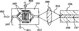
Describe the structure of photomodulator in the past below again in detail.For example shown in figure 32, Mach-Ze De (Mach-Zehnder) type modulator 2012 that is used as photomodulator is for example by LiNbO
3Form on the substrate 2001 that crystal constitutes.Waveguide, the polarization separation that the waveguide part 2002 of this Mach-Ze De type modulator 2012 is included in light incident side does not have the light incident of polarized light (TM light+TE light) 2005 is each waveguide of two polarized lights (TM light and TE light) outgoing and with these polarized lights couplings and the waveguide of outgoing.Wherein, in separatory waveguide place of polarized light the electrode 2003 that applies electric field is set.This electrode 2003 adds the voltage of regulation from signal source 2004.Then, light is penetrated light 2010 and is utilized lens 2009 and optical fiber 2006 couplings.In addition, optical fiber 2006 has fibre core 2007 and covering 2008.Light transmits to a distant place in fibre core 2007.
As mentioned above, in optical devices such as photomodulator in the past,, need lens at least for expensive waveguide and the optical system from photomodulator to optical fiber are coupled.In addition, optical system coupled for this waveguide and optical fiber need expend a large amount of time and manpower.
The following describes optical sensor in the past.Shown in Figure 33 is the front elevation of photoelectric pressure transducer brief configuration in the past.This photoelectric pressure transducer has Sensor section, luminous component, light accepting part branch and emission side and sensitive side signal processing circuit (not shown).This Sensor section is configured in the polarizer 241,1/4 wavelength sheets on the same optical axis (be also referred to as " λ/4 slice ") 242 successively by the light incident side from light, and electro-optic crystal 243 and analyzer 244 constitute.In addition, LightEmitting Diode) (light emitting diode: the E/O circuit of light-emitting component and be configured in the input side optical system that optical fiber 246a, lasso 248a, grin lens 247a and support 245a on the same optical axis form and constitute such as, the axial plane that each optical element of this input side optical system is in contact with one another bonds with cementing agent luminous component by comprising LED as light source.Light accepting part divides the outgoing side optical system of being made up of optical fiber 246b, the lasso 248b, grin lens 247b and the support 245b that are configured on the same optical axis and comprises converting optical signals with this outgoing side optical system outgoing is that the O/E circuit of the inverting element of electric signal constitutes, and each optical element of outgoing side optical system also bonds with cementing agent at the axial plane that is in contact with one another.
In the Sensor section of above-mentioned photoelectric pressure transducer, the axial plane that is in contact with one another that is configured in above-mentioned each optical element on the same optical axis and is the polarizer 241, λ/4 slices 242, electro-optic crystal 243 and analyzer 244 all bonds with cementing agent.Here so-called axial plane is meant the face vertical with optical axis, has the plane of incidence and two axial planes of exit facet (down together) of light for each optical element.Electro-optic crystal 243 evaporation pair of electrodes 235, this pair of electrodes 235 utilize lead-in wire and pair of electrodes terminal 249 to be electrically connected respectively.The voltage of measuring with above-mentioned photoelectric sensor (tested voltage) is added between the terminal of pair of electrodes terminal 249.
Emission side and sensitive side signal processing circuit utilize luminous component and light accepting part branch to be connected with Sensor section respectively.The input side axial plane of the polarizer 241 of Sensor section utilizes the axial plane of the grin lens 247a of cementing agent and luminous component to fix, and the outgoing side axial plane of the analyzer 244 of Sensor section utilizes the axial plane of the grin lens 247b of cementing agent and light accepting part branch to fix.Then, the outgoing side optical system and shell (not shown) mechanical fixation of the input side optical system of bonding fixed sensing part, luminous component and light accepting part branch.In addition, the cementing agent that each optical element is used in the above-mentioned photoelectric pressure transducer uses resins such as epoxy system or polyurethanes.
In above-mentioned photoelectric pressure transducer, electro-optic crystal 243 uses Bi
12SiO
20(BSO), KH
2PO
4(KDP), the LiNbO that has natural birefringence
3And LiTaO
3Deng.
The principle of work of photoelectric pressure transducer is described below with reference to Figure 34.When the light source of luminous component for example used the LED of centre wavelength 0.85 μ m (Light Emitting Diode), the no polarized light of LED penetrated from luminous component, is incident to Sensor section as incident light 109.This incident light 109 becomes linearly polarized light by behind the polarizer 241 of Sensor section.This linearly polarized light then becomes circularly polarized light by λ/4 slices 242, and this circularly polarized light is by electro-optic crystal (LiNbO
3) after 243,243 making alive Vm form ellipse according to this electro-optic crystal, promptly the polarized state of light by electro-optic crystal 243 changes with the making alive Vm of institute.Such elliptically polarized light divides acceptance by behind the analyzer 244 as emergent light 110 usefulness light accepting parts.The Strength Changes of this emergent light 110 is that the output intensity variation is corresponding with the polarized state of light by electro-optic crystal 243.Because this polarization state changes with the making alive Vm of institute, therefore, the output intensity variation of the analyzer 244 in the light accepting part branch is monitored by the optical fiber 246b of sensitive side, calculate the degree of modulation of light quantity (intensity), just can measure the making alive Vm of institute.Here, the degree of modulation of so-called light quantity is the AC component of light quantity and the ratio of the DC component of light quantity.
Photoelectric pressure transducer is used under the outdoor rugged surroundings more, and is very strict for the requirement of its temperature characterisitic, is preferably in-20 ℃ ~ 80 ℃ scopes, and degree of modulation changes below ± 1%.In above-mentioned photoelectric sensor in the past, the principal element that produces temperature characterisitic is the adhesive segment stress in λ/4 plates 242 or the electro-optic crystal 243 and cause the birefringence temperature characterisitic of change of refractive and λ/4 slices 242.In addition, using LiNbO
3When having the electro-optic crystal of natural birefringence, because of being incident to the incident beam state variation of electro-optic crystal 243, the output of photoelectric pressure transducer etc. can change.
Shown in Figure 35 is the partially routine curve map of one of relation of angle beta and photoelectric pressure transducer output of an inclined to one side angle [alpha] and axle.In Figure 35, the β 1 expression axle folk prescription that dotted line is represented is to the situation that is 0,90,180,270 (degree), and the β 2 expression axle folk prescriptions that dot-and-dash line is represented are to the situation that is 45,225 (degree), and the β 3 expression axle folk prescriptions that solid line is represented are to the situation that is 135,315 (degree).As shown in figure 35, because of the incident beam state (axle drift angle α and the inclined to one side angle beta of axle etc.) that is incident to electro-optic crystal 243 changes, the output of photoelectric pressure transducer is that degree of modulation changes, or the temperature characterisitic of its degree of modulation changes.
Correspond respectively to the improvement method of these principal elements, can enumerate following three kinds now.
(1) one of method of being enumerated is by relaxing the temperature characterisitic that stress that electro-optic crystal adds improves electro-optic crystal.Adopting this method, is by fixing electro-optic crystal with unadhered state, relaxing the added stress of electro-optic crystal with this.This method has been opened in the flat 9-145745 communique the spy and has been disclosed.
(2) two of the method for being enumerated is temperature characterisitics of improving the electro-optic crystal natural birefringence by the axle drift angle degree that reduces incident light.Adopting this method is by improving the machining surface accuracy of optical element itself, makes angle of light in the electro-optic crystal below 0.2 °, improves because an inclined to one side temperature characterisitic that causes of incident light with this.This method is opened flat 3-44562 communique the spy and is disclosed.
(3) three of the method for being enumerated is to change corresponding to environment temperature by the incident angle that makes the electrooptic cell incident light, improves the temperature characterisitic of sensor output with this.Adopting this method is to adopt the incident angle adjustment member, the incident angle of electro-optic crystal (bubble Ke Ersi element) incident light is changed corresponding to environment temperature, the output that the output variation that this incident angle is changed and cause causes with temperature variation changes and offsets, and improves the temperature characterisitic that sensor is exported with this.Opened in the flat 7-248339 communique the spy according to the optical sensor of this method and to have disclosed.
As mentioned above, in optical device in the past, optical system coupled for optical fiber needs one or two lens at least, and the part number is also more.In addition, for so optical system coupled, need a large amount of time and manpower.Thereby problem is, if adopt the structure of optical device as described above, will cause the cost of device to rise.
Have again,, except the problems referred to above, also have the distinctive problem relevant with temperature characterisitic to optical sensor.If promptly,, when the incipient beam of light state is variant, can not avoid the variation of temperature characterisitic though can prevent to constitute the light beam state change of very big temperature characterisitic reason according to the method for above-mentioned (1).The method of above-mentioned (2), though use fairly simple, the axle an inclined to one side influence be not only a drift angle degree, the axle folk prescription to relation is also arranged.Therefore only reduce a drift angle degree, can not obtain stable properties according to the method for above-mentioned (2).In the method for above-mentioned (3), need the incident angle adjustment member, the incident angle of electro-optic crystal incident light is changed corresponding to environment temperature, this spline structure is just complicated, causes throughput rate to descend and the cost rising.In addition, as previously mentioned, because a drift angle degree is not only in the inclined to one side influence of axle, the axle folk prescription is to also there being relation, and the incident angle of therefore only adjusting incident light is an axle drift angle degree, can not obtain stable temperature characterisitic.
Applicant to this application is willing to file an application for flat 11-215798 number as the spy with regard to the photoelectric pressure transducer of invention, the method of described photoelectric pressure transducer basis is to utilize the inclined to one side characteristic of electro-optic crystal axle with natural birefringence rate to control the temperature characterisitic of degree of modulation.According to the photoelectric pressure transducer of inventing in this application, be the temperature characterisitic of improving photoelectric pressure transducer by control electro-optic crystal incident beam state (axle drift angle degree and axle folk prescription to or the angle of divergence etc.).Promptly not only consider an axle drift angle degree, also consider the axle folk prescription to, the suitable inclined to one side state of setting shaft is by improving temperature characterisitic etc. like this.
But, to control the light beam state according to the invention in this application, and will the light beam state be managed the discrete of light beam state in order to prevent that tolerance because of optical elements such as lens from causing, cause cost to rise, be disadvantageous therefore to price.
Thereby, now in order to reduce the price of photoelectric pressure transducer, require the light beam state to be managed with low cost.
As mentioned above, the object of the present invention is to provide can be with the optical fiber simple and low-cost optical device cheaply optical system coupled, that part is few that carries out.In addition, other purpose of the present invention also is to provide the light beam discrete state and discrete that does not cause cost to rise and suppress to cause because of optical element tolerance etc., makes the stable optical sensors such as photoelectric pressure transducer of temperature characterisitic with this.
In order to achieve the above object, the present invention has following characteristics.
The 1st aspect of the present invention is the method for making photonic crystal (photonic crystal), aforementioned photonic crystal generation method be end face with at least one optical fiber as substrate, directly form photonic crystal at this end face.For example, should become a bundle by many fibre bundles, the end face separately of many optical fiber is alignd at grade, form fibre bundle, the fibre bundle end face that the end face that aligns on the same plane is constituted is as substrate, direct growth photonic crystal on this substrate is separated into each optical fiber that constitutes fibre bundle with the fibre bundle that forms photonic crystal on the end face again.
The 2nd aspect of the present invention is the method for making photonic crystal, aforementioned photonic crystal generation method is along by the fibre core of transmission light and coat the optical axis of the optical fiber that the covering of this fibre core constitutes, in the interval of regulation, utilize many columns that fibre core is connected, thereby form photonic crystal.For example, in the interval of regulation, remove covering partly, form at least one parallel plane,, fibre core is connected with respect to the vertical many emptying apertures (hole) that form in the plane that in the 1st step, forms along optical axis from optical fiber.
The 3rd aspect of the present invention is the light transmission member, and the aforementioned lights conveying member has that light with a surface feeding sputtering transmits and plays the layer of photonic crystals of line polarizer function from the light to wavelength that the optical fiber of other end outgoing and at least one end face end face of optical fiber and other end form.
The 4th aspect of the present invention is the light transmission member, the aforementioned lights conveying member have that light with a surface feeding sputtering transmits and from another point of view the light that forms of the optical fiber of outgoing and at least one end face in end face of optical fiber and other end to wavelength play the layer of photonic crystals of λ/4 function.
The 5th aspect of the present invention is the light transmission member, the aforementioned lights conveying member have that light with a surface feeding sputtering transmits and from another point of view the light that forms of the optical fiber of outgoing and at least one end face in end face of optical fiber and other end to provision wavelengths play the layer of photonic crystals of round polarizer function, i.e. the photonic crystal circle polarizer.
The 6th aspect of the present invention is an optical device, the aforementioned lights device comprises funtion part and as the hop of the transmission light of fiber functions, the aforementioned functional branch is to connect fibre core along the regulation of optical axis is interval by many columns, forming at least one funtion part as photonic crystal.This funtion part also can by parallel to each other, for constituting with many columns that some cycles distributes perpendicular to the face of its length direction.In addition, the many columns that constitute funtion part also can not only connect fiber core, also connect covering, are made of the material that has with the refractive index different refractivity of the material that forms fibre core.Have again, constitute many columns of funtion part, its all or a part constitute by material with emptying aperture (hole), Faraday effect or material with electrooptical effect.
In addition, on the face that also can form electrode is set partly removing covering.This electrode can be arranged on the face vertical with the many cylinder length directions that constitute funtion part, also can be vertical with the many column length directions that constitute funtion part, and be separately positioned on funtion part is clipped on central two relative parallel surfaces, also can be parallel in addition, and be separately positioned on two parallel surfaces in the middle of funtion part is clipped in the many column length directions and the optical axis that constitute funtion part.Have again, this electrode can be configured to make the direction of funtion part applied field and optical axis parallel to each other, also can be arranged such that with to constitute the many column length directions and the optical axis of funtion part orthogonal, also can be arranged such that along the vertical plane of optical axis to add electric field with predetermined angular with respect to many column length directions.
In addition, funtion part also can comprise the 1st funtion part and the 2nd funtion part that separates the interval setting of regulation along optical axis, the 1st funtion part is made of many columns that the faraday crystal constitutes, the 2nd funtion part is made of many emptying apertures, and the length direction of column and the length direction of emptying aperture are along the vertical plane of optical axis angle at 45.
In addition, also can the 1st funtion part constitute by many columns that electro-optic crystal constitutes, the 2nd funtion part is made of many 1st emptying apertures, and the length direction of the length direction of column and the 1st emptying aperture has perpendicular or parallel a certain relation along the vertical plane of optical axis.
In addition, funtion part also can also comprise the 3rd funtion part that is made of many 2nd emptying apertures, and the length direction of the length direction of column and the 2nd emptying aperture has perpendicular or parallel a certain relation along the vertical plane of optical axis.
In addition, funtion part also can form as the photonic crystal with regulation refractive index and distribution, and the feasible wavelength dispersion characteristics that has can the waveform of the light of broadening reverts to precipitous waveform and outgoing owing to the intrinsic wavelength dispersion characteristics of optical fiber of process before with being incident to optical fiber.
In addition, this optical device also can be provided with the lasso that surrounds around the optical fiber, have other optical fiber that contacts with the optical fiber tubular conduit of diameter about equally.Conduit for example is a kapillary.
The 7th aspect of the present invention is an optoisolator, it is characterized in that, the aforementioned lights isolator has the 1st and the 2nd optical fiber, is close to the faraday element of configuration and the conduit of mechanical adjustment the 1st optical axis and faraday element optical axis and the 2nd optical axis between them, the the aforementioned the 1st and the 2nd optical fiber has the many emptying apertures that distribute with some cycles on interval form parallel to each other and the vertical plane at its length direction along the regulation of optical axis, fibre core is connected, and the emptying aperture length direction of the 1st optical fiber and the emptying aperture length direction of the 2nd optical fiber are along the vertical plane of optical axis angle at 45.
The 8th aspect of the present invention is an optical sensor, it is characterized in that, be to measure alive optical sensor on the electro-optic crystal film according to the light beam that light accepting part divide to be accepted, the aforementioned lights sensor have the emission light beam luminous component, on the regulation optical axis of setting along beam path successively configuration will not have the light accepting part branch of the light beam after circle that polarized light is transformed to circularly polarized light plays the Sensor section of inclined to one side part and electro-optic crystal film and analyzer and acceptance to pass through Sensor section.In this optical sensor, luminous component comprises introduces the 1st optical fiber that Sensor section is used with light beam.The light accepting part branch comprises and will draw the 2nd optical fiber of usefulness from Sensor section by the light beam of Sensor section.Justify part partially and comprised λ/4 slice that no polarized light are transformed to the polarizer of linearly polarized light and linearly polarized light are transformed to circularly polarized light.Here, the polarizer is the layer of photonic crystals of linearly polarized light beam as the optical beam transformation of autoluminescence in future part, form at the 1st fiber end face, analyzer forms at the 2nd fiber end face as being the layer of photonic crystals of linearly polarized light beam by the optical beam transformation of Sensor section.
The 9th aspect of the present invention is an optical sensor, it is characterized in that, be to measure alive optical sensor on the electro-optic crystal film according to the light beam that light accepting part divide to be accepted, the aforementioned lights sensor has the luminous component of emission light beam, configuration will not have the circle that polarized light is transformed to circularly polarized light and play the Sensor section of inclined to one side part and electro-optic crystal film and analyzer and the light accepting part branch that the light beam of Sensor section is passed through in acceptance successively on the regulation optical axis of setting along beam path.In this optical sensor, luminous component comprises introduces the 1st optical fiber that Sensor section is used with light beam.The light accepting part branch comprises and will draw the 2nd optical fiber of usefulness from Sensor section by the light beam of Sensor section.Here, having justified partially, part is the layer of photonic crystals of circularly polarized light beam as autoluminescence in future optical beam transformation partly, form at the 1st fiber end face, analyzer forms at the 2nd fiber end face as being the layer of photonic crystals of linearly polarized light beam by the optical beam transformation of Sensor section.
The 10th aspect of the present invention is an optical sensor, it is characterized in that, be to measure the optical sensor that adds magnetic field on the magneto-optical crystal film according to the light beam that light accepting part divide to be accepted, the aforementioned lights sensor has the luminous component of emission light beam, at the Sensor section that disposes the polarizer and magneto-optical crystal film and analyzer on the regulation optical axis of setting along beam path successively and the light accepting part branch of the light beam after accepting to pass through Sensor section.In this optical sensor, luminous component comprises introduces the 1st optical fiber that Sensor section is used with light beam.The light accepting part branch comprises and will draw the 2nd optical fiber of usefulness from Sensor section by the light beam of Sensor section.Here, the polarizer is the layer of photonic crystals of linearly polarized light beam as the optical beam transformation of autoluminescence in future part, form at the 1st fiber end face, analyzer forms at the 2nd fiber end face as being the layer of photonic crystals of linearly polarized light beam by the optical beam transformation of Sensor section.
The 11st aspect of the present invention is an optical sensor, it is characterized in that, be to divide the light beam of accepting to measure alive optical sensor on the electro-optic crystal according to light accepting part, dispose the polarizer successively on the regulation optical axis that the aforementioned lights sensor has the luminous component of emission light beam, set along beam path, λ/4 slice, the Sensor section of electro-optic crystal and analyzer and accept light accepting part branch by the light beam behind the Sensor section.This optical sensor setting have the reflecting surface vertical with optical axis and be configured in the 1st reflectance coating between λ/4 slice and the electro-optic crystal and have the reflecting surface vertical with optical axis and be configured in electro-optic crystal and analyzer between the 2nd reflectance coating, the 1st reflectance coating and the 2nd reflectance coating be spaced apart half integral multiple of light beam wavelength.
To the following detailed description that the present invention did, these and other objects of the present invention, characteristics and advantage will be more clear from the reference accompanying drawing.
Figure 1 shows that the stereographic map of photonic crystal circle polarizer structure.
Figure 2 shows that photonic crystal method for making as the polarizer, analyzer and circle polarizer function.
Figure 3 shows that other method for making of photonic crystal as the polarizer, analyzer and circle polarizer function.
Figure 4 shows that the photon band figure when fiber core makes the square distribution of cylindrical emptying aperture.
Figure 5 shows that the optical device structural representation of the present invention's the 1st example.
Figure 6 shows that the part-structure synoptic diagram of other example of optical device of the present invention's the 1st example.
Figure 7 shows that the optical device structural representation of the present invention's the 2nd example.
Figure 8 shows that the optical device texture edge synoptic diagram of the present invention's the 3rd example.
Figure 9 shows that the optical device texture edge synoptic diagram of the present invention's the 4th example.
Figure 10 is the overall diagram of the optical device of the present invention's the 5th example.
The perspective illustration of Figure 11 for funtion part shown in Figure 10 78 is amplified from oblique optical fiber 71.
Figure 12 shows that the optical device integral level sectional view of the present invention's the 5th example.
Figure 13 shows that the optical device structural representation of the present invention's the 6th example.
Figure 14 shows that the optical device structural representation of the present invention's the 7th example.
Figure 15 shows that the optical device structural representation of the present invention's the 8th example.
Figure 16 shows that the optical device structural representation of the present invention's the 9th example.
Figure 17 shows that the optical device structural representation of the present invention's the 10th example.
Figure 18 shows that the diagrammatic cross-section of electrode configuration example in the optical device of the present invention's the 11st example.
Figure 19 shows that the optical device horizontal sectional drawing of the present invention's the 12nd example.
Figure 20 shows that the photovoltage sensing arrangement synoptic diagram of the present invention's the 13rd example.
Shown in Figure 21 is temperature characteristics figure, respectively the photoelectric pressure transducer output that causes of the temperature characterisitic of the quartzy system of expression λ/4 slice change, the LiNbO of electro-optic crystal
3The photoelectric pressure transducer output of vertical modulation system of causing of temperature characterisitic change and the LiNbO of electro-optic crystal
3The photoelectric pressure transducer output of the horizontal modulation system that causes of temperature characterisitic change.
Shown in Figure 22ly be the conductive reflecting film in the photoelectric pressure transducer of the present invention's the 14th example.
Conductive reflecting film for constituting for stacked multilayer film with low-index layer and high index of refraction floor height in the photoelectric pressure transducer of the present invention's the 15th example shown in Figure 23.
Shown in Figure 24 for the photoelectric pressure transducer major part structure front perspective view of the present invention's the 16th example.
Shown in Figure 25 for the photoelectric pressure transducer major part structure front perspective view of the present invention's the 17th example.
Shown in Figure 26 for the photoelectric pressure transducer major part structure front perspective view of the present invention's the 18th example.
Shown in Figure 27 for the photoelectric pressure transducer major part structure front perspective view of the present invention's the 19th example.
Shown in Figure 28 for the photoelectric pressure transducer major part structure front perspective view of the present invention's the 20th example.
Shown in Figure 29 for the magneto-optical sensor major part structure front perspective view of the present invention's the 21st example.
Shown in Figure 30 for the photoelectric pressure transducer major part structure front perspective view of the present invention's the 22nd example.
Optical device in the past shown in Figure 31 is the optical isolator structure synoptic diagram.
Shown in Figure 32 is in the past Mach-Ze De type modulator structure synoptic diagram.
Shown in Figure 33 is in the past photoelectric pressure transducer structure front perspective view.
Figure 34 is a photoelectric pressure transducer principle of work key diagram.
Shown in Figure 35ly be the performance plot of output in the photoelectric pressure transducer in the past with the relation of the incident light axis drift angle degree that is incident to electro-optic crystal.
Before the optical device structure that describes each example in detail, at first the photonic crystal to utilizations such as the polarizer that constitutes each optical device (the line polarizer and the circle polarizer), analyzer, λ/4 slice, bubble Ke Ersi elements carries out brief description, and its formation method is described simultaneously.
<form as the photonic crystal of line polarizer function
Document about photonic crystal, " Photonic crystal (photonic crystal) " that An Nuobo network this (John D.Joannopoulos), Mead (Robert D.Meade) and the temperature (Josua N.Winn) of for example having an appointment collaborateed is by Princeton University publishing house (Princeton University Press) distribution (nineteen ninety-five distribution).As described in the document, photonic crystal has the periodic structure of the 1-3 dimension that is made of relative high-index material and low-index material, be the interior light wave dispersion characteristics of aforementioned periodic structure of utilizing mainly spatial variations cycle, incident beam direction and wavelength because of the refractive index of high-index material and low-index material and shape, refractive index (below be called " use beam direction " reach " use light beam wavelength ") to cause, light wave is controlled.Thereby, if for using light beam wavelength, the spatial variations cycle of aforementioned refractive index in the suitable control photonic crystal and shape, refractive index and use beam direction, then two kinds of linearly polarized lights are TM ripple and TE ripple dispersion characteristics produce differences, utilize this phenomenon just can realize the polarizer and λ/4 slice.For example, for the polarizer that utilizes such photonic crystal, opened in the 2000-56133 communique and disclosed the spy.In addition, about the high-index material of photonic crystal use and the shape of low-index material, document is described like that as described above, proposes many kinds of schemes and makes.
Thereby the 18th example etc. is used as described later, can form layer of photonic crystals as the line polarizer and analyzer function at fiber end face.Promptly when fiber end face forms the layer of photonic crystals that is made of high-index material and low-index material, can set the spatial variations cycle of the refractive index of high-index material and low-index material and shape, refractive index and use beam direction for this light wavelength, make the TM that light comprised that in this optical fiber, will transmit involve only a kind of ripple in the TE ripple by this layer of photonic crystals (for example with reference to special open Fig. 4 and Fig. 6 that the 2000-56133 communique is put down in writing).To narrate in the back the photonic crystal formation method that fiber end face is concrete.
In addition, in the 13rd example described later, when making by this two-layer alternately laminated and multilayer film of constituting of so-called high refractive index layer and low-index layer as photonic crystal, if it is stacked along the incident light direction (optical axis direction) that is incident to Sensor section to set these two kinds of layers, and the thickness sum of the thickness of high refractive index layer and low-index layer is 1/4 of this lambda1-wavelength, then just can make TM involve the TE ripple like this and all can not pass through this layer of photonic crystals.This means, play the function of reflectance coating as the multilayer film of 1 dimensional photonic crystal formation for this incident light.About the structure of the concrete optical device that adopts such function, will narrate in the corresponding in the back example.
<form as the photonic crystal of λ/4 function
As mentioned above, if for using light beam wavelength, suitable spatial variations cycle of aforementioned refractive index in the control photonic crystal and shape, refractive index and use beam direction, two kinds of dispersion characteristics generation differences that linearly polarized light is TM ripple and TE ripple then utilize this phenomenon just can realize λ/4 slice.Thereby the 19th example etc. is described as described later, can form luminescent crystal layer as λ/4 function at fiber end face.I.e. when fiber end face forms the layer of photonic crystals that is made of high-index material and low-index material (specifically form method will in aftermentioned), can set the spatial variations cycle of the refractive index of high-index material and low-index material and shape, refractive index and use beam direction for this light wavelength, make and involve the TE ripple by the TM that light comprised that in this optical fiber, will transmit the two all passes through this layer of photonic crystals, and this by after between TM ripple and TE ripple, produce 1/4 the phase differential that is equivalent to this light wavelength.
<form as the layer of photonic crystals of circle polarizer function
The polarizer that no polarized light is transformed to circularly polarized light is promptly justified the polarizer, can utilize at optical propagation direction and be realized by the photonic crystal with 1-3 dimension periodic structure that relative high magnetic permeability and low magnetic permeability material constitute.
Figure 1 shows that stereographic map as one of photonic crystal of justifying polarizer function example.This photonic crystal periodically disposes the cylindrical part that is made of high-permeability material in low magnetic permeability medium (for example air), by having high magnetic permeability part 211 and low magnetic permeability part 212 like this, promptly has the periodic structure that the 2 dimension cycles of magnetic permeability change (below be called " 2 dimension periodic structures of magnetic permeability ") with the periodic structure that some cycles 2 dimensions repeat.In addition, as long as high magnetic permeability part 211 there is no need at the magnetic permeability of all directions all high high with respect to the magnetic permeability of the incident light direction of propagation that is incident to this 2 dimensional photonic crystal 210.In addition, as long as low magnetic permeability part 212 there is no need at the magnetic permeability of all directions all low low with respect to the magnetic permeability of the incident light direction of propagation that is incident to this 2 dimensional photonic crystal 210.
Now, be not incident to photonic crystal 210 with such magnetic permeability 2 dimension periodic structures (below should no polarized light be called " no polarized incident light ") if there is polarized light, as shown in Figure 1, if 2 dimensional photonic crystals 210 dispose like this, make magnetic permeability cycle variation on the direction of propagation of this no polarized incident light 215 and at least one direction vertical with this direction of propagation.No polarized incident light 215 generally can be decomposed into the right-circularly polarized light 213 of electric field intensity right-hand screw rotation and the left circularly polarized light 214 of electric field intensity left-hand screw rotation.The magnetic field (below this magnetic field ripple being called " the 2nd magnetic field ripple ") of magnetic field of right-circularly polarized light 213 (below this magnetic field ripple being called " the 1st magnetic field ripple ") and left circularly polarized light 214 is all parallel to each other reverse along the direction of propagation of no polarized incident light 215.If for the wavelength of no polarized incident light 215 suitably magnetic permeability, the magnetic permeability of the high magnetic permeability part 211 in setting 2 dimensional photonic crystals 210 and low magnetic permeability part 212 the spatial variations cycle and do not have the direction of polarized incident light 215, then at the border generation reflex time of the high magnetic permeability part 211 of the 1st and the 2nd magnetic field ripple in 2 dimensional photonic crystals 210 with low magnetic permeability part 212, the phase differential after phase place before this reflection and the reflection is different for the 1st magnetic field ripple and the 2nd magnetic field ripple.If the difference of the phase differential that produces satisfies defined terms like this.Then for a certain side in the 1st and the 2nd magnetic field ripple, scattering is to work weakening this magnetic direction, and to the opposing party, and scattering is to work strengthening this magnetic direction.As a result, with identical as the aforementioned photonic crystal of line polarizer function, only a certain square tube in the 1st and the 2nd magnetic field ripple is crossed 2 dimensional photonic crystals 210.Thereby, magnetic permeability by high magnetic permeability part 211 in suitable setting 2 dimensional photonic crystals 210 and low magnetic permeability part 212, the spatial variations cycle of magnetic permeability and do not have the direction of polarized incident light 215, can make this 2 dimensional photonic crystal 210 for the function of no polarized incident light 215, obtain circular polarization emergent light 216 as the circle polarizer.Thereby the 20th example is such as described later, can form the layer of photonic crystals (specifically forming method will narrate in the back) of the conduct circle polarizer function of individual layer at fiber end face.
The formation of layer of photonic crystals on the<fiber end face 〉
The following describes the method for on fiber end face, making photonic crystal.Fig. 2 is the photonic crystal method for making key diagram with periodic structure of 3 dimension high index of refraction particulates 221 and low-refraction part 222 formations.In this generation method, as described below, be to form photonic crystal 223 at fiber end face.In addition, describe, equally also can make photonic crystal with magnetic permeability periodic structure though just have the photonic crystal making of refractive index cycle structure below.
(1) at first many fibre bundles is become a bundle, an end face of each optical fiber is alignd at grade substantially, constitute fibre bundle 224.
(2) as mentioned above, the end face of the fibre bundle 224 that each end face is alignd at grade substantially and constitute is as substrate, the stacked high index of refraction particulate 221 of periodicity on this substrate, this high index of refraction particulate 221 has the 20-80% left and right sides particle diameter of the light beam wavelength (use light beam wavelength) that transmits with these optical fiber.
(3) as mentioned above, the fibre bundle 224 of the stacked high index of refraction particulate 221 of end face periodicity is separated into the optical fiber of a rule.
Utilize above-mentioned steps (1)-(3), can produce the optical fiber that forms photonic crystal on the end face in batches.Certainly, the quantity of fibre bundle 224 without limits, its quantity also can be one, though this is not suitable for producing in batches.
The cross section of drawn fiber core 2 has approximate identical size with high index of refraction particulate 221 in Fig. 2, but common fibre core diameter is 5-300 μ m, and when using light beam wavelength to be 0.85 μ m, the particle diameter of high index of refraction particulate 221 is 0.17-0.68 μ m.In addition, in photonic crystal shown in Figure 2 223, low-refraction part 222 is an air, but identical with above-mentioned steps (2), after stacked particulate, also can be in the gap between this particulate the filling refractive index greater than this particulate refractive index materials.In this case, the photonic crystal that obtains has stacked aforementioned particulate part as the low-refraction part, with the material of filling between the aforementioned particulate periodic structure as the high index of refraction part.In addition, photonic crystal 223 shown in Figure 2 has high index of refraction part and the alternately repeated periodic structure of low-refraction part, but also can be same as described above, form photonic crystal with high magnetic permeability part and the alternately repeated periodic structure of low magnetic permeability part at fiber end face.
According to the method for the stacked high index of refraction particulate 221 of above-mentioned steps (1)-(3) periodicity, high index of refraction particulate 221 is uniformly-spaced typically to arrange with the figure of rule.But, on fiber end face, make high index of refraction particulate 221 with the regulation pattern arrangement the time, then also need to add in addition step.
For example, in step (2), before stacked high index of refraction particulate 221, be increased in the step that fiber end face forms desirable groove pattern.After forming groove pattern like this, if stacked high index of refraction particulate 221 then can be arranged high index of refraction particulate 221 according to this figure, fiber facet forms the photonic crystal with desired structure relatively.
Here, so-called groove pattern is meant for high index of refraction particulate 221 being separately fixed at the set of the set shallow slot of assigned position.The width of groove and the degree of depth do not have special restriction.In addition, if high index of refraction particulate 221 can be separately fixed at the figure of assigned position, then being not limited to groove shape figure certainly, can be the figure that 1 or 2 above wire or point-like projection constitute, and also can be the figure that point-like or planar pit constitute.
As the concrete grammar that forms above-mentioned groove pattern at fiber end face, can consider for example to have following three kinds.First method is, after forming PMMA resin moldings such as (polymethacrylate) on the substrate, utilizes the desirable groove pattern of electron beam drawing with spin-coating method etc., then by developing, forms groove pattern.The 2nd kind of method is the mask of the desirable groove pattern of configuration on substrate, carries out removing mask after the corrosion treatment and forms figure.The 3rd kind of method is to the defeat precision metallic mould that tightly have desirable groove pattern of substrate with regulation, thereby forms groove pattern.
In addition, the fiber end face of formation photonic crystal 223 shown in Figure 2 is perpendicular to the central shaft of fiber core 3, but different with the stacked direction (direction of growth) of above-mentioned photonic crystal 223 sometimes directions meets top condition (or ideal conditions).Promptly for example under the situation of fiber end face formation as the photonic crystal of polarizer function, with the stacked direction setting of this photonic crystal for the time from the inconsistent prescribed direction of the exit direction of this end face light of the optical fiber incident direction of the light of this end face (or be incident to), this photonic crystal has best or desirable function as the polarizer sometimes.At this moment, at first for example utilize oblique grinding that fiber end face is processed, make the end face that form photonic crystal form the angle of regulation with respect to the central shaft (in Fig. 3 described later, being the optical axis 225 of fibre core 173) of fiber core 3.Promptly as shown in Figure 3, make and have the optical fiber 148 that is processed into angled end-face 226, make the angle of normal direction and optical axis 225 meet above-mentioned top condition.Then, identical with above-mentioned steps (2), at the stacked high index of refraction particulate 221 of normal direction 227 periodicity of this angled end-face 226.Form at the angled end-face 226 of optical fiber 148 like this and have particulate 221 as the high index of refraction part, the air that the gap of 221 of particulates is existed is as the photonic crystal of the periodic structure of low-refraction part 222.
In addition, also can be as above-mentioned step (1)-(3), many the optical fiber 148 that form angled end-face 226 are restrainted into a bundle, make each angled end-face 226 alignment at grade, constitute fibre bundle, after then this fibre bundle angled end-face being formed photonic crystal as mentioned above, this fibre bundle is separated into a rule optical fiber.If like this, just can produce the optical fiber of on angled end-face 226, making photonic crystal in batches.
In addition, when the oblique stacked photonic crystal of the optical axis 225 of relative optical fiber 148 shown in Figure 3 is carried out optical coupled with the optical element with face vertical with optical axis 225, can use angled end-face, but also can be on oblique this stacked photonic crystal coating resin etc., formation is perpendicular to the end face of optical axis 225, makes the end face of optical fiber 148 of laminated photon crystal and the face of this optical element be adjacent to.
The situation of making 3 dimensional photonic crystals at fiber end face more than has been described, but form on the vertical or angled end-face with respect to optical axis is not to have 3 dimension periodic structures, but when stacked direction has 1 dimensional photonic crystal of this multi-layer film structure of periodic structure, also can adopt and use the same method.
Layer of photonic crystals in the<optical fiber forms 〉
The following describes the photonic crystal method for making in optical fiber.In order to make optical fiber connect with fibre core and covering, form the many cylindrical emptying aperture that is parallel to each other, this cylindrical emptying aperture distributes at regular intervals.Cylindrical emptying aperture like this, for example by with respect to the vertical direction of optical axis with mechanical treatments such as drill bits, with optical processing or thermal treatments such as laser, form with chemical treatments such as corrosion, form the many small emptying aperture that connects fibre core.For example, the dry etching of anodised aluminium oxide as mask corroded in employing.In the cylindrical emptying aperture that forms like this, the gas that can be full of air or have various refractive indexes also can utilize for example sol-gal process filling to have the material of arbitrary refractive index.Here, if the material of filling is functional materials such as faraday crystal or liquid crystal, then this part in the optical fiber just has the polarizer, faraday element according to the character of functional material, function such as λ/4 slice.Concrete method for making about optical fiber with these functions will be narrated in each example in the back.
The photonic crystal that above-mentioned many cylindrical emptying apertures constitute is relevant with the distribution of emptying aperture.Figure 4 shows that the photon frequency band that makes in the fiber core when cylindrical emptying aperture is square to distribute according to the simulation result gained.In Fig. 4, transverse axis is for to launch corresponding to the omnirange of transmission direction in Brillouin zone (Brillouin zone) of light.In addition, the longitudinal axis is corresponding to normalized frequency.Solid line is represented the light of TM mould, and dotted line is represented the light of TE mould.In addition, the wave-number vector in the Brillouin zone of transverse axis is corresponding to the transmission direction of the light in the optical fiber, and the normalized frequency of the longitudinal axis is corresponding to optical source wavelength.
In the example of Fig. 4,,, be merely able to transmit the light of TE mould in any case can not there be the light of TM mould for the optical source wavelength in TM mould forbidden band.And as can be known, the transmission direction that the light of this TE mould allows is limited to certain transmission direction, and columniform emptying aperture is distributed, and the direction that makes this TE mould to transmit is consistent with optical axis.This optical device can have the function that only makes the polarizer of TE mould transmission with the optical source wavelength of this frequency band for certain transmission direction.Thereby, if columniform emptying aperture is distributed, make that the transmission direction that constitutes the polarizer is consistent with the optical axis of optical fiber, then optical fiber also plays the effect of the polarizer near the pattern of transmitting the optical axis.
In addition, photon frequency band shown in Figure 4 is as an example that makes under the columniform emptying aperture distribution situation, but is not limited thereto.For example, forming under the cylindrical situation, this cylindrical material refractive index of formation is changed with the columniform emptying aperture of various material fillings.Thereby, according to different conditions such as the refractive index of cylindrical emptying aperture part, external diameter, distributions, also can play not only the TE mould whole transmission directions, and the polarizer function that the TM mould is had.
Like this, have refractive index different and many cylindrical emptying aperture parallel to each other as if forming at certain intervals with fiber core refractive index in vertical direction with respect to optical axis, then except the optical waveguide function of optical fiber, the distribution of refractive index, external diameter and cylindrical emptying aperture by controlling cylindrical emptying aperture, just produce the difference of the dispersion characteristics of two kinds of linearly polarized lights (TM and TE) for optical source wavelength, can have the function of the polarizer or λ/4 slice etc.In addition, the shape of emptying aperture is not limited to cylindrical, also can be other shape.Below shown in each example be the example of various optical devices being used said methods.
Below the optical device of each example along by the fibre core of transmission light and surround certain interval of the optical axis that covering constituted of this fibre core, have two funtion parts that constitute by the 1st funtion part and the 2nd funtion part, perhaps have three funtion parts that also comprise the 3rd funtion part.These funtion parts separate the certain intervals setting along optical axis.The 1st funtion part is many columns perforation optical fiber parallel to each other of being formed by the material of refractive index different refractivity that has with the material that forms aforementioned fibre core or its fibre core and constitute.Specifically, for example filling has the material of electrooptical effect or has the material of Faraday effect.The the 2nd and the 3rd funtion part is that inner many columns perforation fibre cores parallel to each other for emptying aperture constitute.Owing to have these funtion parts, this optical device makes each dispersion characteristics of two kinds of linearly polarized lights (TM and TE) produce difference, just can make each funtion part have functions such as the polarizer, λ/4 slice, faraday element.
(the 1st example)
The present invention's the 1st example is described with reference to the accompanying drawings.Fig. 5 (a) is depicted as the side schematic view of the optical device structure of the present invention's the 1st example.Fig. 5 (b) is the diagrammatic cross-section that the optical device line B-B ' position in the drawings with Fig. 5 (a) vertically cuts with respect to optical axis 2.Fig. 5 (c) is the diagrammatic cross-section that the optical device line C-C ' position in the drawings with Fig. 5 (a) vertically cuts with respect to optical axis 2.In Fig. 5 (a), be only to take out the regulation segment part corresponding shown in the optical fiber 1 with optical device.
Shown in Fig. 5 (a), this optical device forms on optical fiber 1, and optical fiber 1 is made of the fibre core 3 of transmission light and the covering 4 that surrounds this fibre core 3.In addition, in optical fiber 1, form two funtion parts that constitute by the 1st funtion part 7 and the 2nd funtion part 8, have the optical device function.The 1st funtion part 7 and the 2nd funtion part 8 separate the predetermined distance setting along the optical axis 2 of optical fiber 1.In addition, in optical fiber 1, the part except that the above-mentioned functions part only realizes that the common function of optical fiber is the light transmission function.
At first, the 1st funtion part 7 is to be made of many faraday crystal displacement cylinders 5 parallel to each other that the vertical direction with respect to optical axis 2 forms in the certain interval along the optical axis 2 of optical fiber 1, to make the fibre core 3 of optical fiber 1 and covering 4 connect.These many faraday crystal displacement cylinders 5 are to respect to the fibre core 3 and cylindrical emptying aperture that covering 4 connect of optical axis 2 vertical direction with optical fiber, for example utilize sol-gal process, and filling has the faraday crystal of the refractive index different with fibre core 3 refractive indexes and constitutes.The faraday crystal for example is a garnet crystal etc.In addition, this faraday crystal displacement cylinder 5 distributes separately on respect to the vertical plane of its length direction and forms dot matrix.Here, for the faraday rotation that makes polarization surface saturated, with the optical axis 2 parallel magnetic fields 20 that have sufficient intensity of optical fiber 1.
Secondly, the 2nd funtion part 8 is to be that many emptying apertures 6 parallel to each other in cavity constitute in the inside that the certain interval along the optical axis 2 of optical fiber 1 is formed by the vertical direction with respect to optical axis 2, makes the fibre core 3 and covering 4 perforations of optical fiber 1.These many emptying apertures 6 are also identical with faraday crystal displacement cylinder 5, and distributing separately on respect to the vertical plane of its length direction forms dot matrix.But the length direction that the length direction of these many emptying apertures 6 is set at along the plane perpendicular to optical axis 2 with respect to the faraday crystal displacement cylinder 5 of the 1st funtion part 7 has 45.This cylindrical emptying aperture 6 is by for example natural filling air, also has the different refractive index of refractive index with the fibre core 3 of optical fiber 1.
The faraday crystal displacement cylinder 5 of the 1st funtion part 7 and the cylindrical emptying aperture 6 of the 2nd funtion part 8 are in the situation of 45, if compare and can understand with reference to Fig. 5 (b) and Fig. 5 (c).
Further describe the 1st and the 2nd funtion part 7 and 8 below again.Cylinder with refractive index different with the refractive index of the fibre core 3 of optical fiber 1 can utilize methods such as drill bit, laser or corrosion to form in the vertical direction with respect to the optical axis 2 of optical fiber 1 as previously mentioned.The 1st funtion part 7 is that the many faraday crystal displacement cylinders 5 that form by so cylindrical emptying aperture that forms is utilized sol-gal process filling faraday crystal constitute, and has the function of the polarizer and faraday element simultaneously.And the 2nd funtion part 8 only is made of many emptying apertures 6, in order to make it have the function of the polarizer (analyzer), calculate the distribution of the external diameter and the emptying aperture 6 of emptying aperture 6 in advance, will with the direction at the length direction angle at 45 of the faraday crystal of the 1st funtion part 7 displacement cylinder 5 as length direction, form emptying aperture 6 like this.
Like this if having the many cylindrical emptying aperture parallel to each other of the refractive index different or the cylinder of filling functional material in this emptying aperture forming at certain intervals with the refractive index of fibre core 3 with respect to the vertical direction of optical axis 2, then for optical source wavelength, by control emptying aperture or cylinder refractive index, external diameter and emptying aperture or cylinder distribution, make the dispersion characteristics of two kinds of linearly polarized lights (TM and TE) produce difference.As a result, because the 1st funtion part 7 in the optical fiber 1 forms the polarizer and faraday element, the 2nd funtion part 8 forms analyzer, so optical fiber 1 also has the effect of optoisolator except the optical waveguide function.Thereby the operation that can not need the waveguide with lens and optoisolator to be coupled can also reduce the part number simultaneously, can realize reducing cost significantly.
Fig. 6 is other example part-structure synoptic diagram of the optical device of the present invention's the 1st example.Emptying aperture 6 shown in Figure 6 can be the emptying aperture 6 that the 2nd funtion part 8 is comprised among Fig. 5 (a), also can be to form faraday crystal column precipitator 5 emptying aperture before.
In aforesaid explanation, form the emptying aperture of cylindrical emptying aperture 6 or faraday crystal displacement cylinder 5 usefulness, be to make to comprise that covering 4 also connects and the emptying aperture that forms, but as shown in Figure 6, also can be only form emptying aperture in the part of fibre core 3.This is because actual glazing only passes at the fibre core 3 of optical fiber 1 inside, no matter be that cylindrical emptying aperture comprises covering 4 and connects, also no matter be fibre core 3 only, pass the influence that the light of optical fiber 1 inside is subjected to and does not almost change.
In addition, the shape of emptying aperture describes with cylindrical in the 1st example, but is not limited to cylindrically, also can be other shape such as four side column shapes, polygon cylindricality or elliptical cylinder-shape.In addition, above-mentioned functions is to realize with 2 dimensional photonic crystals that the many emptying apertures that are parallel to each other or cylinder constitute in the above-mentioned explanation, but be not limited to this situation, also can realize with having 3 dimensional photonic crystals that are called Ya Buluonuobaiyite (yablonovite) or Wood Pai Yier (woodpile) structure.
(the 2nd example)
The present invention's the 2nd example is described with reference to the accompanying drawings.Fig. 7 (a) is depicted as the side schematic view of the optical device structure of the present invention's the 2nd example.Fig. 7 (b) is the diagrammatic cross-section that the optical device line B-B ' position in the drawings with Fig. 7 (a) vertically cuts with respect to optical axis 2.Fig. 7 (c) is the diagrammatic cross-section that the optical device line C-C ' position in the drawings with Fig. 7 (a) vertically cuts with respect to optical axis 2.In Fig. 7 (a), be only to take out the regulation segment part corresponding shown in the optical fiber 1 with optical device.
As shown in Figure 7, this optical device by have fibre core 45 and covering 46 and with the incident side optical fibers 41 of light incident, have fibre core 45 and covering 46 and with the exiting side optical fiber 42 of light outgoing, be arranged between incident side optical fibers 41 and the exiting side optical fiber 42 and make the faraday element 47 of polarization surface rotation and the conduit 48 that the optical axis of the optical axis of the optical axis of incident side optical fibers 41 and faraday element 47 and exiting side optical fiber 42 carries out mechanical adjustment is constituted.Faraday element 47 for example is a garnet crystal.
Incident side optical fibers 41 has many cylindrical the 1st emptying aperture 43 parallel to each other that forms in the vertical direction with respect to optical axis 49 in the certain interval along optical axis 49, fibre core 45 and covering 46 are connected.The 1st emptying aperture 43 distributes at certain intervals, have with optical fiber 41 in the different refractive index of refractive index of fibre core 45.
Equally, exiting side optical fiber 42 has many cylindrical the 2nd emptying aperture 44 parallel to each other in the vertical direction formation of relative optical axis 49 in the certain interval along optical axis 49, and fibre core 45 and covering 46 are connected.The 2nd emptying aperture 44 also distributes at certain intervals, have with optical fiber 42 in the different refractive index of refractive index of fibre core 45.
Here about the 1st emptying aperture 43 and the 2nd emptying aperture 44, as illustrating in the 1st example, distribute separately many 1st emptying apertures 43 and many 2nd emptying apertures 44 have the effect of the polarizer.About the configuration of the 1st and the 2nd emptying aperture 43 and 44, as shown in Figure 4, as long as periodic distribution.In addition, compare as can be known with reference to Fig. 7 (b) and Fig. 7 (c), the direction setting of the direction of the 1st emptying aperture 43 and the 2nd emptying aperture 44 is that mutual length direction differs 45 °.Here relevant with faraday 47, saturated for the faraday rotation that makes polarization surface, there is the magnetic field 40 of the sufficient intensity parallel with respect to optical axis 49.
In addition, identical about the formation method of the 1st and the 2nd emptying aperture 43 and 44 with the 1st example, utilizing drill bit, laser or corrosion to form emptying aperture with respect to the vertical direction of optical axis 49.
Yet, in this example, utilize conduit 48 that incident side optical fibers 41 and exiting side optical fiber 42 are mechanically connected, they can be rotated freely around optical axis 49 separately.Thereby, when in conduit 48, adjusting optical axis, also can adjust angle, make the 2nd emptying aperture 44 relative formation 45s in the 1st emptying aperture 43 and the exiting side optical fiber 42 in the incident side optical fibers 41.Constitute according to such optical fiber, can form the 2nd emptying aperture 44 in the 1st emptying aperture 43 and the exiting side optical fiber 42 in the incident side optical fibers 41 equally, and mutual relative angle is as long as adjust afterwards, so can reduce manufacturing cost.
In addition, in aforesaid explanation, the cylindrical emptying aperture of formation be will comprise the optical fiber of covering 46 connect, but identical with the situation of Fig. 6, also can be only form emptying aperture in the part of fibre core 45.In addition, the materials such as faraday crystal that also can filling in the 1st emptying aperture 43 or the 2nd emptying aperture 44 have the refractive index different with the refractive index of each fiber core 45.Here, in the 1st emptying aperture 43 or the 2nd emptying aperture 44, during filling faraday crystal, also can omit faraday element 47.
Have, the shape of emptying aperture describes with cylindrical in the 2nd example again, but is not limited to cylindrically, also can be other shape such as four side column shapes, polygon cylindricality, elliptical cylinder-shape.In addition, in the above-mentioned explanation, above-mentioned functions is to realize with 2 dimensional photonic crystals that the many cylinders that are parallel to each other constitute, but is not limited to this situation, also can realize with having 3 dimensional photonic crystals that are called Ya Buluonuobaiyite or Wood Pai Yier structure.Have again, also can adopt the layer of photonic crystals that forms at the end face of incident side optical fibers 41 and exiting side optical fiber 42, replace the 1st emptying aperture 43 in the incident side optical fibers 41 and the 2nd emptying aperture 44 in the exiting side optical fiber 42.About the method for making photonic crystal at fiber end face, for example use Fig. 2, generate the method for the photonic crystal that constitutes by 3 dimension high index of refraction particulates 221 and low-refraction part 222 with periodic structure, this narrates in front.
Like this, only optical fiber is formed the same processing of emptying aperture, just can form the polarizer and analyzer, with the faraday element with have the optical fiber combination of the polarizer and analyzer effect, by just constituting optoisolator like this.Thereby the operation that can not need the waveguide with lens and optoisolator to be coupled can also reduce the part number simultaneously, can realize reducing cost significantly.
(the 3rd example)
The present invention's the 3rd example is described with reference to the accompanying drawings.Figure 8 shows that the optical device texture edge synoptic diagram of the present invention's the 3rd example.In addition, in Fig. 8, be only to take out the regulation segment part corresponding shown in the optical fiber 51 with optical device.
As shown in Figure 8, this optical device is by optical fiber 51, respectively producing the pair of electrodes 59 of electric field and an electrode 59 is being added that the signal source 50 of assigned voltage constitutes with respect to the vertical side of optical axis 52.Optical fiber 51 is made of the fibre core 53 of transmission light and the covering 54 that surrounds this fibre core 53.In addition, in optical fiber 51, form two funtion parts that constitute by the 1st funtion part 57 and the 2nd funtion part 58, have the optical device function.The 1st funtion part 57 and the 2nd funtion part 58 separate the interval setting of regulation along the optical axis 52 of optical fiber 51.
At first, the 1st funtion part 57 is to be made of the many bubble Ke Ersi crystal displacement cylinders 55 that are parallel to each other that the vertical direction with respect to optical axis 52 forms in the certain interval along the optical axis 52 of optical fiber 51, makes the fibre core 53 of optical fiber 51 and covering 54 connect.This bubble Ke Ersi crystal displacement cylinder 55 distributes separately on respect to the vertical plane of its length direction and forms dot matrix.And these many bubble Ke Ersi crystal displacement cylinders 55 are that cylindrical emptying aperture is adopted for example sol-gal process filling bubble Ke Ersi crystal and forms.This bubble Ke Ersi crystal has known it is the material that shows an electrooptical effect, for example can adopt LiNbO
3Crystal, LiTaO
3Crystal, NH
4H
2PO
4Crystal and KH
2PO
4Crystal etc.
Secondly, the 2nd funtion part 58 is to be that many emptying apertures 56 parallel to each other in cavity constitute in the inside that the certain interval along the optical axis 52 of optical fiber 51 is formed by the vertical direction with respect to optical axis 52, makes the fibre core 53 and covering 54 perforations of optical fiber 51.These many emptying apertures 56 also distribute to form dot matrix separately on the face vertical with respect to its length direction, have the different refractive index of refractive index with the fibre core 53 of optical fiber 51.
Further describe the 1st and the 2nd funtion part 57 and 58 below again.Cylinder with refractive index different with the refractive index of the fibre core 53 of optical fiber 51 can utilize methods such as drill bit, laser or corrosion to form in the vertical direction with respect to the optical axis 52 of optical fiber 51 as previously mentioned.The 1st funtion part 57 is made of such bubble Ke Ersi crystal displacement cylinder that forms, and has the function of the polarizer and bubble Ke Ersi element simultaneously.And the 2nd funtion part 58 only is made of many emptying apertures 56, in order to make it have the function of the polarizer (analyzer), calculate the distribution of the external diameter and the emptying aperture 56 of emptying aperture 56 in advance, along vertical plane with respect to optical axis 52, with respect to the displacement of the bubble Ke Ersi crystal in the 1st funtion part cylinder 55, vertical or parallel formation emptying aperture 56.About the configuration of emptying aperture, as long as have foregoing periodic structure in Fig. 4 explanation.
Have again,, utilize signal source 50 to come the size of control electrode 59 applied fields, make the variations in refractive index of bubble Ke Ersi crystal displacement cylinder 55 in order to make bubble Ke Ersi crystal displacement cylinder 55 also have the effect of λ/4 slice.In addition, signal source 50 can make electrode 59 added electric field cyclical variations.So, because therefore the variations in refractive index of bubble Ke Ersi crystal displacement cylinder 55 can make the change in optical signal that sees through the 1st funtion part 57.
Like this because as long as optical fiber 51 is processed, just can form the polarizer, steep the Ke Ersi element, λ/4 slice and analyzer, so optical fiber 51 has the effect of photomodulator.Thereby the operation that can not need the waveguide with lens and photomodulator to be coupled can also reduce the part number simultaneously, can realize reducing cost significantly.
In addition, in above stated specification, cylindrical emptying aperture is to make to comprise that covering 54 also connects and the emptying aperture that forms, but identical with the situation of Fig. 6, also can be only forms emptying aperture in the part of fibre core 53.In addition, the emptying aperture shape describes with cylindrical, but is not limited to cylindrically, also can be other shape such as four side column shapes, polygon cylindricality or elliptical cylinder-shape.In addition, in the above-mentioned explanation, above-mentioned functions is to realize with 2 dimensional photonic crystals that the many cylinders that are parallel to each other constitute, but is not limited to this situation, also can realize with having 3 dimensional photonic crystals that are called Ya Buluonuobaiyite or Wood Pai Yier structure.
(the 4th example)
The present invention's the 4th example is described with reference to the accompanying drawings.Figure 9 shows that the optical device side schematic view of the present invention's the 4th example.In addition, in Fig. 9, be only to take out the regulation segment part corresponding shown in the optical fiber 61 with optical device.
As shown in Figure 9, this optical device is by optical fiber 61, produce the electrode 63 of electric field and electrode 63 is added that the signal source 60 of electric field constitutes in the vertical direction with respect to the optical axis 62 of optical fiber 61.Optical fiber 61 is made of the fibre core 83 of transmission light and the covering 84 that surrounds this fibre core 83.In addition, in optical fiber 61, form three funtion parts that constitute by the 1st funtion part the 67, the 2nd funtion part 68 and the 3rd funtion part 69, have the optical device function.The the 1st to the 3rd funtion part 67-69 separates the interval setting of regulation along the optical axis 62 of optical fiber 61.
Here the 1st funtion part 67 of this example is identical with the 1st funtion part 57 of the 3rd example, constitute at the many bubble Ke Ersi crystal displacement cylinders 64 parallel to each other that form by the vertical direction of relative optical axis 62 along certain interval of the optical axis 62 of optical fiber 61, make the fibre core 83 of optical fiber 61 and covering 84 connect.
In addition, the the 2nd and the 3rd funtion part 68 of this example and 69 identical with the 2nd funtion part 58 of the 3rd example, in certain interval along the optical axis 62 of optical fiber 61, the inside that is formed by the vertical direction with respect to optical axis 62 is that empty the many 1st and the 2nd emptying aperture 65 and 66 parallel to each other constitutes, and makes the fibre core 83 of optical fiber 61 and covering 84 connect.This many 1st and the 2nd emptying aperture 65 and 66 distribute to form dot matrix separately on the face vertical with respect to its length direction, have the different refractive index of refractive index with the fibre core 83 of optical fiber 61.In addition, the 1st and the 2nd emptying aperture 65 and 66 is along vertical or be arranged in parallel with respect to the displacement of the bubble Ke Ersi crystal in the 1st funtion part 67 cylinder 64 perpendicular to the plane of optical axis 62.
Further describe the 1st to the 3rd funtion part 67-69 below again.Cylinder with refractive index different with the refractive index of the fibre core 83 of optical fiber 61 can utilize methods such as drill bit, laser or corrosion to form in the vertical direction with respect to the optical axis 62 of optical fiber 61 as previously mentioned.The 1st funtion part 67 is made of such bubble Ke Ersi crystal displacement cylinder 64 that forms, and has the function of the polarizer and bubble Ke Ersi element simultaneously.And the 2nd funtion part 68 only is made of many 1st emptying apertures 65, in order to make it have the function of λ/4 slice, calculate the distribution of the external diameter and the 1st emptying aperture 65 of the 1st emptying aperture 65 in advance, with respect to the displacement of the bubble Ke Ersi crystal in the 1st funtion part 67 cylinder 64, vertical or parallel formation the 1st emptying aperture 65.About the configuration of emptying aperture, if as aforementioned among Fig. 4 period profile.In addition, the 3rd funtion part 69 is also identical with the 2nd funtion part 68, in order to make its function with the polarizer (analyzer), with respect to the displacement of the Bo Keersi crystal in the 1st funtion part 67 cylinder 64, perpendicular or parallel formation the 2nd emptying aperture 66.
Have, signal source 50 makes electrode 59 added electric field cyclical variations again, makes the variations in refractive index of bubble Ke Ersi crystal displacement cylinder 55, by making the change in optical signal that sees through the 1st funtion part 67 like this.
Like this because as long as optical fiber 61 is processed, just can form the polarizer, steep the Ke Ersi element, λ/4 slice and analyzer, so optical fiber 61 has the effect of photomodulator.Thereby the operation that can not need the waveguide with lens and photomodulator to be coupled can also reduce the part number simultaneously, can realize reducing cost significantly.
In addition, in above stated specification, cylindrical emptying aperture is to make to comprise that covering 84 also connects and the emptying aperture that forms, but identical with the situation of Fig. 6, also can be only forms emptying aperture in the part of fibre core 83.In addition, the emptying aperture shape describes with cylindrical, but is not limited to cylindrically, also can be other shape such as four side column shapes, polygon cylindricality or elliptical cylinder-shape.In addition, in the above-mentioned explanation, above-mentioned functions is to realize with 2 dimensional photonic crystals that upright parallel mutually many cylinders constitute, but is not limited to this situation, also can realize with having 3 dimensional photonic crystals that are called Ya Buluonuobaiyite or Wood Pai Yier structure.
(the 5th example)
Below with reference to figure explanation the present invention the 5th example.Figure 10 is the optical device overall diagram of the present invention's the 5th example.The perspective illustration of Figure 11 for funtion part shown in Figure 10 78 is amplified from oblique optical fiber 71.
As shown in figure 11, this optical device forms in optical fiber 71, and optical fiber 71 is made of the fibre core 75 of transmission light and the covering 76 that surrounds this fibre core 75.In addition, in optical fiber 71, form funtion part 78, have the optical device function.
Funtion part 78 is in the certain interval along the optical axis 72 of optical fiber 71, and the inside that is formed by the vertical direction with respect to optical axis 72 is that many emptying apertures 77 parallel to each other in cavity constitute, and makes the fibre core 75 of optical fibre optical fibre 71 and covering 76 connect.These many emptying apertures 77 distribute separately on respect to the vertical plane of its length direction and form dot matrix, have the different refractive index of refractive index with the fibre core 75 of optical fiber 71.This emptying aperture 77 can utilize drill bit in the vertical direction with respect to the optical axis 72 of optical fiber 71 as previously mentioned, and methods such as laser or corrosion form.
Like this, if form many cylindrical emptying aperture parallel to each other at certain intervals with refractive index different with the refractive index of fibre core 75 in vertical direction with respect to optical axis 72, then for optical source wavelength, distribute by control cylinder refractive index, external diameter and cylinder, to the dispersion characteristics generation difference of two kinds of linearly polarized lights (TM and TE).As a result, funtion part 78 is had makes leading wavelength lag behind, make the leading such dispersion characteristics of wavelength of hysteresis.Like this, if can make the phase velocity of optical source wavelength accelerates or slows down, then can form following such wavelength dispersion characteristics, promptly because the signal 79a of the intrinsic wavelength dispersion characteristics of optical fiber and broadening, returns to the such precipitous pulse signal 79b of incident light 73 by after the funtion part 78.Thereby, because emergent light 74 becomes the such signal of incident light 73, so this optical device has the function of dispersion compensator.
Like this, as long as optical fiber 71 is processed, optical fiber 71 just has the effect of dispersion compensator.Thereby the operation that can not need the waveguide with lens and photomodulator to be coupled can also reduce the part number simultaneously, can realize reducing cost significantly.
In addition, in above stated specification, cylindrical emptying aperture is to make to comprise that covering 76 also connects and the emptying aperture that forms, but identical with the situation of Fig. 6, also can be only forms emptying aperture in the part of fibre core 75.In addition, the emptying aperture shape describes with cylindrical, but is not limited to cylindrically, also can be other shape such as four side column shapes, polygon cylindricality or elliptical cylinder-shape.In addition, in the above-mentioned explanation, above-mentioned functions is to realize with 2 dimensional photonic crystals that the many cylinders that are parallel to each other constitute, but is not limited to this situation, also can realize with having 3 dimensional photonic crystals that are called Ya Buluonuobaiyite or Wood Pai Yier structure.But, when optical fiber 71 is the optical fiber of plane of polarization preservation type,, therefore realize unsatisfactory with 3 dimensional photonic crystals because orientation becomes problem.
(to the concrete installation form of optical fiber)
In the example below, specify the situation that optical device such as photomodulator and optical fiber are installed.In the example below, utilize part to remove the plane that covering forms, it is to be relatively easy to that many columns perforation fibre cores parallel to each other are formed.In addition, owing to can electrode be set, therefore can add uniform and stable electric field in funtion part at this covering removal face.To be described in detail below.
(the 6th example)
The present invention's the 6th example is described with reference to the accompanying drawings.Figure 12 shows that the light body integral level sectional view of the present invention's the 6th example.Figure 13 (a) is the side sectional view that a part shown in Figure 12 is amplified.The diagrammatic cross-section that Figure 13 (b) vertically cuts with respect to optical axis 2 for the optical device line B-B ' position in the drawings with Figure 13 (a).
As Figure 12 and shown in Figure 13, this optical device is made of optical fiber 1 and the kapillary 12 that coats around this optical fiber 1.Optical fiber 1 is made of the fibre core 3 of transmission light and the covering 4 that surrounds this fibre core 3.In addition, this optical fiber 1 has two funtion parts that are made of the 1st funtion part 7 and the 2nd funtion part 8.The 1st funtion part 7 and the 2nd funtion part 8 separate the predetermined distance setting along the optical axis 22 of optical fiber 1.Owing to have these funtion parts, this optical device makes each dispersion characteristics of two kinds of linearly polarized lights (TM and TE) that incident light 16 comprised produce difference, therefore can be as the polarizer etc.
Here, the the 1st and the 2nd funtion part 7 of this example and 8 identical with the 1st and the 2nd funtion part 57 and 58 of the 3rd example, therefore the bubble Ke Ersi crystal displacement cylinder 55 of right cylinder 19 of this example and emptying aperture 6 and the 3rd example and emptying aperture 56 same formation and distribution omit the explanation of relevant these parts.But right cylinder 19 and emptying aperture 6 are configurations parallel to each other.
Here, optical fiber 1 eliminates part 18 at the interval covering of removing of regulation in order to form the 1st and the 2nd funtion part 7 and 8, and it is to remove from optical fiber 1 both sides that covering eliminates part 18, until with fibre core 3 almost till the position contacting.The result forms fibre core 3 is clipped in central side section parallel to each other is rectangular pair of parallel boundary surface 23.Thereby shown in Figure 13 (b), optical fiber 1 is in the drawings the remaining up and down covering residual fraction 21 that does not eliminate in the regulation interval, presents the shape of the part about it of pruning, and pair of parallel boundary surface 23 is exposed outside.Adopt such method, just can be easy to form right cylinder 19 and emptying aperture 6.
Then, the many right cylinders 19 that are made of bubble Ke Ersi crystal that constitute the 1st funtion part 7 are added that the pair of electrodes 9 of electric field is arranged on the above-mentioned parallel edges interface 23.This electrode 9 is arranged on the side of optical fiber 1, and the applied field direction is parallel with many right cylinder 19.Like this, owing to configured electrodes 9 on pair of parallel boundary surface 23, therefore can be easy to and correctly add electric field to right cylinder 19.In addition, this electrode 9 is added that the signal source 10 of voltage is arranged on the outside of kapillary 12, a side of electrode 9 is connected with ground wire 11.
In addition, the kapillary 12 around the clad optical fiber 1 has the lasso 14 approximately equalised external diameters with other optical fiber 13 of wanting to be connected.Therefore, when this optical fiber being wanted be connected with other optical fiber 13, with split coupling 15 lasso of kapillary 2 with other optical fiber compressed, it is identical to be coupled with the optical system between optical fiber, make optical axis alignment, therefore can be easy to optical system is coupled.
(the 7th example)
The present invention's the 7th example is described with reference to the accompanying drawings.Figure 14 (a) is depicted as the optical device side schematic view of the 7th example.The diagrammatic cross-section that Figure 14 (b) vertically cuts with respect to optical axis 2 for the optical device line B-B ' position in the drawings with Figure 14 (a).
As shown in figure 14, the optical device of this optical device and the 6th example shown in Figure 13 has essentially identical structure, but parallel pole 24 the position is set and shape different with the electrode 9 of the 6th example.The parallel pole 24 of this example is characterised in that, the parallel pole 24 that is provided with is parallel to each other in the optical axis 22 of optical fiber 1, and be vertical with respect to the length direction of right cylinder 19, it is vertical making applied field like this with respect to the length direction of the many right cylinders 19 that are made of this crystal of bubble gram that constitute the 1st funtion part 7, and also is vertical with respect to optical axis 22.Promptly shown in Figure 14 (a), on the vertical face with respect to the length direction of right cylinder 19, at the upper and lower settings pair of parallel electrode 24 of many right cylinders 19, this point is different with the situation of electrode 9.In addition, the vertical face of so-called length direction with respect to right cylinder 19, shown in Figure 14 (b), be remove that covering eliminates that part 18 results form fibre core 3 is clipped in central pair of parallel boundary surface 23 parallel to each other, its side section is a rectangle.Certainly, because pair of parallel electrode 24 is provided with at grade, therefore not necessarily need as shown in Figure 14 (b), the removal covering eliminates part 18 from about the optical fiber 1, forms two planes (pair of parallel boundary surface 23).Thereby, also can remove covering and eliminate part 18, make only to form the some planes that dispose parallel pole 24 usefulness.Utilize the parallel pole 24 of configuration as mentioned above, can adjust the optical modulation function of the 1st funtion part 7 that many right cylinders 19 of being formed by bubble Ke Ersi crystal are constituted.
In addition, this parallel pole 24 is added that the signal source 10 of voltage is arranged on the outside of kapillary 12, the another side of parallel pole 24 is connected with ground wire 11, and this point is identical with the optical device of example 6, therefore omits its explanation.
(the 8th example)
The present invention's the 8th example is described with reference to the accompanying drawings.Figure 15 (a) is depicted as the optical device side schematic view of the 8th example.The diagrammatic cross-section that Figure 15 (b) vertically cuts with respect to optical axis 2 for the optical device line B-B ' position in the drawings with Figure 15 (a).
As shown in figure 15, the optical device of this optical device and the 6th example shown in Figure 13 has essentially identical structure, but vertically electrode 25 the position is set and shape different with the electrode 9 of the 6th example.The vertical electrode 25 of this example is characterised in that, the vertical electrode 25 that is provided with is parallel with the optical axis 22 of optical fiber 1, and be vertical with respect to the length direction of right cylinder 19, it is vertical and parallel with respect to optical axis 22 with respect to the length direction of the many right cylinders 19 that are made of bubble Ke Ersi crystal that constitute the 1st funtion part 7 to make institute's making alive like this.Promptly shown in Figure 15 (a), on vertical plane, 1 pair of vertical electrode 25 is set about many right cylinders 19 with respect to the length direction of right cylinder 19, this point is different with the situation of electrode 9.In addition, what is called is the pair of parallel boundary surface 23 shown in Figure 15 (b) with respect to the vertical face of the length direction of right cylinder 19 as previously mentioned.Certainly, because a pair of vertical electrode 25 is provided with at grade, therefore not necessarily need as shown in Figure 15 (b), the removal covering eliminates part 18 from about the optical fiber 1, forms two planes (pair of parallel boundary surface 23).Thereby, also can remove covering and eliminate part 18, make only to form the some planes that dispose vertical electrode 25 usefulness.Utilize the vertical electrode 25 of configuration as mentioned above, can adjust the optical modulation function of the 1st funtion part 7 that many right cylinders 19 of being formed by bubble Ke Ersi crystal are constituted.
In addition, this vertical electrode 25 is added that the signal source 10 of voltage is arranged on the outside of kapillary 12, and vertically the another side of electrode 25 is connected with ground wire 11, and this point is identical with the optical device of example 6, therefore identical component part additional phase symbol together, and omit its explanation.
(the 9th example)
The present invention's the 9th example is described with reference to the accompanying drawings.Figure 16 (a) is depicted as the optical device side schematic view of the 9th example.The diagrammatic cross-section that Figure 16 (b) vertically cuts with respect to optical axis 2 for the optical device line B-B ' position in the drawings with Figure 16 (a).
As shown in figure 16, the optical device of this optical device and the 6th example shown in Figure 13 has essentially identical structure, but eliminates covering 4 again, in addition comparative electrode 26 that the position is set is different with the electrode 9 of the 6th example.
At first, shown in Figure 16 (b), optical fiber forms the 1st and the 2nd funtion part, for comparative electrode 26 is set, eliminate part 18 at the interval covering of removing of regulation, it is to remove about reaching up and down from optical fiber 1 that covering eliminates part 18, until with fibre core 3 almost till the position contacting.The result forms respectively about fibre core 3 and up and down fibre core 3 is clipped in central side section parallel to each other is rectangular a pair of the 1st parallel edges interface 31 and the 2nd parallel edges interface 32.Thereby, shown in Figure 16 (a), optical fiber 1 surrounds fibre core 3 at the interval remaining covering residual fraction 21 that does not eliminate of regulation, and presenting with optical axis 22 is the tetragonal prism shape of central shaft, and a pair of the 1st parallel edges interface 31 and a pair of the 2nd parallel edges interface 32 are exposed outside.Adopt such method, just can be easy to form right cylinder 19 and emptying aperture 6, can on the plane different, comparative electrode 26 be set simultaneously with the situation of the 6th example.
Then, it is characterized in that, the comparative electrode 26 that setting is parallel to each other and also parallel with respect to the length direction of right cylinder 19 with respect to the optical axis 22 of optical fiber 1, to make comparative electrode 26 with respect to many right cylinders 19 length directions that are made of bubble Ke Ersi crystal that constitute the 1st funtion part 7 vertical and optical axis 22 is also vertically added electric field.Promptly shown in Figure 16 (a) and Figure 16 (b), at parallel with respect to the length direction of right cylinder 19 and also parallel face with respect to optical axis 22, be on a pair of the 2nd parallel edges interface 23, at a pair of comparative electrode 26 of the upper and lower settings of many right cylinders 19, this point is different with the situation of electrode 9.Utilize the parallel pole 24 of configuration like this, can adjust the optical modulation function of the 1st funtion part 7 that many right cylinders 19 of being formed by bubble Ke Ersi crystal constitute.
In addition, this comparative electrode 26 is added that the signal source 10 of voltage is arranged on the outside of kapillary 12, and the another side of comparative electrode 26 is connected with ground wire 11, and this point is identical with the optical device of example 6, therefore identical component part additional phase symbol together, and omit its explanation.
(the 10th example)
The present invention's the 10th example is described with reference to the accompanying drawings.Figure 17 (a) is depicted as the optical device side schematic view of the 10th example.The diagrammatic cross-section that Figure 17 (b) vertically cuts with respect to optical axis 2 for the optical device line B-B ' position in the drawings with Figure 17 (a).
Shown in Figure 17 (a), the optical device of the 9th example shown in this optical device and Figure 16 (a) has essentially identical structure, but the length direction of emptying aperture 6 is different with the 6th example.Be that this example optical device is characterised in that, many right cylinders 19 its length directions of the 1st funtion part 7 that formation optical fiber 1 is provided with are orthogonal with the length direction of the many emptying apertures 6 that constitute the 2nd funtion part 8.Specifically, shown in Figure 17 (b), the length direction of right cylinder 19 is along the horizontal direction of figure, and the length direction of emptying aperture 6 is the above-below directions along figure.
As mentioned above, the length direction that utilize to constitute the right cylinder 19 of the 1st and the 2nd funtion part 7 and 8 and emptying aperture 6 is orthogonal, can adjust the effect of the optical modulation function of each funtion part.
In addition, the situation with two funtion parts has been described above, but such, has had the situation of three funtion parts, can be suitable for too for the optical device of the 4th example.
(the 11st example)
The optical device of the present invention's the 11st example is characterized in that, the electrode that applies electric field is arranged to direction of an electric field and constitutes angulation θ between the length direction of column of the 1st funtion part.Owing to make the length direction of column and direction of an electric field form certain angle θ like this, just can adjust the optical modulation function of the 1st funtion part.
The optical device of this optical device and the 9th or the 10th example relatively, in the transverse section of the optical fiber 1 shown in Figure 18 (a), the parallel pole 87 that applies electric field is arranged to the length direction angulation θ of direction of an electric field and the right cylinder 19 that constitutes the 1st funtion part 7, and this point is inequality.Specifically, in the regulation interval, remove covering 4 basically, remaining fibre core 3 is contacting with fibre core 3 or the position of adosculation is provided with pair of parallel electrode 87, makes the length direction angulation θ of itself and right cylinder 19.In addition, this optical device also can adopt being similar to along the curved surface electrode 88 of the curved surface bending of fibre core 3 shown in Figure 18 (b), replaces the parallel plate electrode 87 shown in Figure 18 (a).When adopting curved surface electrode 88, set curved surface electrode 88 and make the length direction of right cylinder 19 and the normal direction 35 angulation θ of curved surface central authorities.
(the 12nd example)
The optical device of the present invention's the 12nd example is characterized in that, the many right cylinders that form with the crystal by having Faraday effect that connects fibre core constitute first funtion part of optical fiber.Because such the 1st funtion part constitutes with the right cylinder that the crystal with Faraday effect forms, and therefore by adding magnetic field, just can adjust the faraday rotation angle of the 1st funtion part.Thereby this light body has insulator functionality.
Figure 19 shows that the optical device horizontal sectional drawing of the present invention's the 12nd example.This optical device as shown in figure 19, with the photomodulator of the 6th example relatively, many right cylinders 91 that it forms with the crystal by having Faraday effect of perforation fibre core 3 constitute the 1st funtion part of optical fiber 1, this point is inequality.Specifically, the right cylinder that constitutes the 1st funtion part 7 is not with bubble Ke Ersi crystal but with the crystal formation with Faraday effect.Crystal with this Faraday effect can be used for example garnet crystal, rare earth, iron garnet crystal (YIG etc.).Be provided with in the outside of kapillary 12 again and add the magnet 95 in magnetic field 94 or embed magnet when the processing outside having crystal that this method connects younger brother's effect.Magnet 95 is so long as permanent magnet such as rare earth element magnet or electromagnet etc. so long as to produce the faraday rotation of the plane of polarisation that the magnetic field of sufficient intensity makes light saturated substantially, then can be used any magnet.In addition, because faraday rotation angle and magnetic direction are irrelevant, therefore, can select the various directions that apply magnetic field 94.
The example that<optical sensor is relevant 〉
In the example below, specify the structure and the principle of work of optical sensors such as the relevant photoelectric pressure transducer of the present invention, photocurrent sensor, magneto-optical sensor.
(the 13rd example)
The photoelectric pressure transducer of the present invention's the 13rd example at first is described.
The photoelectric pressure transducer of this example, as shown in figure 20, have Sensor section, luminous component 118 and light accepting part and divide 119, Sensor section is played successively by the light incident side of light that the polarizer 101, λ/4 the 102, the 1st conductive reflecting film 106, electro-optic crystal the 103, the 2nd conductive reflecting film 107 and the analyzer 104 of configuration constitute on same optical axis 108.
Sensor section disposes the above-mentioned polarizer 101, λ/4 the 102, the 1st conductive reflecting film 106, electro-optic crystal the 103, the 2nd conductive reflecting film 107 and analyzer 104 successively on the light path of its light beam, this light beam utilizes these optical elements, penetrates with tested voltage Vm modulation back.In this example, use the LiNbO of Z axle transmission
3Crystal is as electro-optic crystal 103, and electro-optic crystal 103 is configured to make its Z axle (C axle) consistent with optical axis 108.In addition, the 1st conductive reflecting film 106 and the 2nd conductive reflecting film 107 dispose like this, make their reflecting surface vertical, and the interval dr of the 1st conductive reflecting film 106 and the 2nd conductive reflecting film 107 is half the integral multiple of wavelength that is incident to the incident light 109 of Sensor section with optical axis 108.In addition, set coordinate system as shown in figure 20, make the Z axle along optical axis 108, X-axis and Y-axis mutually perpendicular both direction in the plane vertical respectively with optical axis 108.At this moment, the LiNbO that transmits with respect to the Z axle
3When crystal added electric field along Z-direction, when promptly vertically modulating, the electro-optic constant relevant with degree of modulation was γ 33 and γ 31, at the LiNbO of Z axle transmission
3When the direction initialization of crystal 103 was X-direction, the direction initialization of the polarizer 101 and analyzer 104 was ± 45 ° with respect to X-axis.The direction initialization of λ/4 slices 102 is X-direction or Y direction.Here so-called direction initialization is meant the major axes orientation in ellipse garden of expression refractive index, and described refractive index is the refractive index for the light beam that is incident to electro-optic crystal or λ/4 slice etc.
Light accepting part divides 119 by the outgoing side optical system that comprises optical fiber etc. and to comprise converting optical signals be that the O/E circuit of the components of photo-electric conversion of electric signal constitutes.Through the outgoing side optical system, be subjected to light by the light beam of Sensor section outgoing, be transformed to electric signal with the components of photo-electric conversion in the O/E circuit.This electric signal is and passes through LiNbO
3Light beam polarization state behind the crystal 103 is corresponding, and this polarization state changes according to tested voltage Vm.Utilize and divide the 119 sensitive side signal processing circuits (not shown) that are connected,, calculate degree of modulation, by obtaining tested magnitude of voltage like this according to this electric signal with light accepting part.
The concrete structure of the photoelectric pressure transducer of Gou Chenging for example is the described structure of Figure 24 described later or Figure 30 as mentioned above.About the details of these structures,, therefore omit its detailed description here owing to will describe as other example in the back.
The photoelectric pressure transducer of this example, as previously mentioned, the 1st conductive reflecting film 106 of Sensor section and the interval dr of the 2nd conductive reflecting film 107 are set at half the integral multiple of wavelength of the incident light 109 that is incident to Sensor section.If set like this, between the 1st conductive reflecting film 106 and the 2nd conductive reflecting film 107, constitute standard resonator (being also referred to as " Fabry-Pei Luo resonator ").Therefore, be that the light of the direction transmission of optical axis 108 plays dominating role along the vertical direction of the 1st conductive reflecting film 106 and the 2nd conductive reflecting film 107, as shown in figure 20, it is 115 very precipitous that beam angle distributes.That is to say, even because of the tolerance of optical element or structural error etc. cause the center position of incident light 109 or are distributed with difference, but effect owing to the standard resonator that constitutes by the 1st conductive reflecting film 106 and the 2nd conductive reflecting film 107, light by electro-optic crystal 103, its center position vertical with reflecting surface (parallel) with optical axis 108, so its distribution is also certain.Again because the effect of such standard resonator is also certain by the light wavelength of electro-optic crystal 103.
According to this above-mentioned example, utilize the standard resonator that constitutes by the 1st conductive reflecting film 106 and the 2nd conductive reflecting film 107, the center position of the light by electro-optic crystal 103 and distribute then certain.The incident beam that promptly is incident to electro-optic crystal 103 is with in stable condition by the light beam of the light beam behind the electro-optic crystal 103.Even the result causes that because of the tolerance of optical element etc. the light beam state of the incident light 109 that is incident to Sensor section is variant, and that the output of the photoelectric pressure transducer of this example is degree of modulation is still stable.In addition, center position as if the incident light 109 that is incident to Sensor section is variant, the beam intensity that then is incident to electro-optic crystal 103 changes, but because that it distributes is certain, the difference of center position that therefore is incident to the incident light 109 of Sensor section divides the AC component of light income in 119 and the difference that the DC component compares the degree of modulation that is drawn not to have materially affect for light accepting part.
In addition, because the distribution 115 of above-mentioned beam angle is relevant with the reflectivity of the 1st conductive reflecting film 106 and the 2nd conductive reflecting film 107, reflectivity is high more, and beam angle distribution 115 is more little, and therefore best reflectivity is more than 0.6.Like this, if beam angle distribution 115 reduces, then, just can access certain characteristic for the inclined to one side characteristic of axle that causes because of birefringence as shown in Figure 35.
In above-mentioned example, be the LiNbO that adopts for the transmission of Z axle
3Crystal 103 is that the direction of optical axis 108 adds vertical modulation system of electric field in Z-direction, but also can adopt the LiNbO for the transmission of Z axle
3Crystal 103 adds in X-direction and the horizontal modulation system of electric field replaces vertical modulation system.As the concrete structure of the photoelectric pressure transducer of horizontal modulation system, for example can enumerate the structure (with reference to Figure 25) that will be described hereinafter
When adopting horizontal modulation system, the electro-optic constant relevant with the degree of modulation of photoelectric pressure transducer is γ 22, at the LiNbO of Z axle transmission
3When the direction initialization of crystal film 103 was X-direction, the direction initialization of the polarizer 101 and analyzer 104 was X-direction or Y direction, and the direction initialization of λ/4 slices 102 is ± 45 ° with respect to X-axis.Because the temperature characterisitic of electro-optic constant γ 22 is little, therefore under the situation of horizontal modulation system, the output of photoelectric pressure transducer (degree of modulation) is with in the variation of temperature (below be called " output is with variation of temperature "), because LiNbO
3The temperature characterisitic of crystal 103 influence composition, as shown in phantom in Figure 21, reach almost negligible degree (the photoelectric pressure transducer output (degree of modulation) the when longitudinal axis is represented with 25 degrees centigrade among Figure 21 be the relative output variation of benchmark).But because the birefringent temperature characterisitic of λ/4 slices 102, laterally the output of the photoelectric pressure transducer of modulation system is that degree of modulation has temperature characterisitic.But, as mentioned above, owing to surrounding LiNbO
3Formation standard resonator in the zone of crystal film 103, light beam is in stable condition, therefore even cause that because of the tolerance of optical element etc. the light beam state of the incident light 109 that is incident to Sensor section is variant, the output temperature characteristic of photoelectric pressure transducer is indifference also, is stable.According to this situation, when adopting horizontal modulation system, also can be used for temperature sensor.
Shown in above-mentioned example, when adopting vertical modulation system, as previously mentioned, be that the relevant electro-optic constant of degree of modulation is γ 33, γ 31, at the LiNbO of Z axle transmission with the output of photoelectric pressure transducer
3When the direction initialization of crystal 103 was X-direction, the direction initialization of the polarizer 101 and analyzer 104 was ± 45 ° with respect to X-axis, and the direction initialization of λ/4 slices 102 is X-direction or Y direction.Under the situation of vertical modulation system, because the temperature characterisitic of electro-optic constant γ 33 and γ 31, during the Yin Wendu of photoelectric pressure transducer and the output that produces change, by LiNbO
3The temperature characterisitic of crystal 103 influence composition, in Figure 21 shown in the with dashed lines.Even temperature rises, because LiNbO
3The temperature characterisitic of the crystal 103 and output of photoelectric pressure transducer is descended.In addition, there is the composition that the birefringence temperature characterisitic because of λ/4 slices 102 causes (below this being called " output that the temperature characterisitic of λ/4 slices 102 causes changes ") during the Yin Wendu of photoelectric pressure transducer and the output that produces change.Yet, the ellipse for the refractive index of its incident light of expression λ/4 slices 102 (below be called " refractive index ellipse "), temperature is high more, approaches proper circle more.On the other hand, expression LiNbO
3The ellipse (refractive index ellipse) for the refractive index of its incident light of crystal 103, temperature is high more, becomes flat ellipse more.Thereby, if make the leading phase shaft direction and the LiNbO of the refractive index ellipse of λ/4 slices 102
3The leading phase shaft direction unanimity of the refractive index ellipse of crystal 103, the sensor output and the relation of temperature that then causes because of both temperature characterisitics cancel each other (with reference to the straight line of dotted line among Figure 21 and solid line), as a result, the Yin Wendu of photoelectric pressure transducer and the output that causes change and reduce.Be LiNbO
3When the direction initialization of crystal 103 was X-direction, the direction initialization of λ/4 slices 102 also was set at X-direction, by improving the output temperature characteristic of photoelectric pressure transducer like this.
(the 14th example)
The following describes the photoelectric pressure transducer of the present invention's the 14th example.
Photoelectric pressure transducer of this example and the 13rd example have essentially identical structure, promptly have structure shown in Figure 20.In the photoelectric pressure transducer inscape of this example,, and omit its explanation for the inscape additional phase identical reference marks together with the 13rd example.In addition, the principle of work that the photoelectric pressure transducer of this example is whole, since also identical in essence with the 13rd example, so omit its detailed description.
In this example, as shown in figure 22, realize with the multilayer film that reflectance coating and transparent and electrically conductive film constitute at the conductive reflecting film that Sensor section formation standard resonator is used.It is the 1st conductive reflecting film 106 in above-mentioned the 13rd example, in this example, realize (representing the 1st conductive reflecting film) with this example of this multilayer film realization with reference marks 106b with the multilayer film that the 1st transparent and electrically conductive film 121 and the 1st reflection mould 122 constitute.In addition, the 2nd conductive reflecting film 107 in above-mentioned the 13rd example, in this example, implement (representing the 2nd conductive reflecting film) with this example of this multilayer film realization with reference marks 107b with the multilayer film that the 2nd transparent and electrically conductive film 123 and the 2nd reflectance coating 124 constitute.Thereby in this example, the interval dr2 of the 1st reflectance coating 122 and the 2nd reflectance coating 124 is set to be incident to half the integral multiple of wavelength of the incident light 109 of Sensor section.The the 1st and the 2nd transparent and electrically conductive film 121 and 123 can use for example ITO (Indium-Tin-Oxide) (indium-tin-oxide) film etc.
In addition, shown in Figure 22 is that the 1st transparent and electrically conductive film 121 that constitutes the 1st conductive reflecting film 106b all is configured in LiNbO with the 2nd transparent and electrically conductive film 123 that constitutes the 2nd conductive reflecting film 107b
3The example of crystal (electro-optic crystal) 103 1 sides, but the 1st transparent and electrically conductive film 121 and the order of the 1st reflectance coating 122 and the order of the 2nd transparent and electrically conductive film 123 and the 2nd reflectance coating 124 are arbitrarily.No matter their order how, the interval of the 1st reflectance coating 122 and the 2nd reflectance coating 124 will be configured to be incident to half the integral multiple of wavelength of the incident light 109 of Sensor section but as mentioned above.
According to this example, the 1st conductive reflecting film 106b and the 2nd conductive reflecting film 107b that utilization realizes with the multilayer film that transparent and electrically conductive film and reflectance coating constitute, identical with the 13rd example, constitute the standard resonator, like this center position of the light by electro-optic crystal 103 and distribute certain.As a result, even because of the tolerance of optical element etc. causes that the light beam state of the incident light 109 that is incident to Sensor section is variant, the output of the photoelectric pressure transducer of this example is that degree of modulation is also stable.Have again, according to this example, because the 1st conductive reflecting film 106b and the 2nd conductive reflecting film 107b realize with the multilayer film that transparent and electrically conductive film and reflectance coating constitute, therefore when forming the 1st and the 2nd conductive reflecting film 106b and 107b, can control their conductance and reflectivity respectively.Thereby, compare with the situation of utilizing monofilm realization conductive reflecting film, owing to can be easy to form the big conductive reflecting film of reflectivity, therefore can more improve the above-mentioned in stable condition effect of light beam that makes.
(the 15th example)
The following describes the present invention's the 15th example photoelectric pressure transducer.
Photoelectric pressure transducer of this example and the 13rd example have essentially identical structure, promptly have structure shown in Figure 20.In the photoelectric pressure transducer inscape of this example,, and omit its explanation for the inscape additional phase identical reference marks together with the 13rd example.In addition, the principle of work that the photoelectric pressure transducer of this example is whole, since also identical in essence with the 13rd example, so omit its detailed description.
In this example, be LiNbO with electro-optic crystal 103 at Sensor section
3Crystal film be clipped in central and the configuration two conductive reflecting films, realize with multilayer film shown in Figure 23.It is the 1st conductive reflecting film 106 in above-mentioned the 13rd example, in this example, constitute (representing like this in this example the 1st conductive reflecting film) with the 1st transparent and electrically conductive film 121 and the 1st multilayer film 133 formations with reference marks 106c with the 1st transparent and electrically conductive film 121 and the 1st multilayer film 133 with reflectance coating function.In addition, the 2nd conductive reflecting film 107 in above-mentioned the 13rd example, in this example, constitute (the 2nd conductive reflecting film of using reference marks 107c table in this example, to constitute like this) with the 2nd transparent and electrically conductive film 123 and the 2nd multilayer film 134 with the 2nd transparent electrical film 123 and the 2nd multilayer film 134 with reflectance coating function.The 1st multilayer film 133 and the 2nd multilayer film 134 all be along optical axis 108 directions by high refractive index layer 131 and the alternately laminated multilayer film that forms of low-index layer 132 these two kinds of book layers, have refractive index along the periodically variable periodic structure of optical axis 108 directions.Promptly the 1st multilayer film 133 and the 2nd multilayer film 134 are 1 dimensional photonic crystals.In addition, in this example, the 1st transparent and electrically conductive film 121 is clipped in the 1st multilayer film 133 and LiNbO
3Between the crystal film 103, the 2nd transparent and electrically conductive film 123 is clipped in the 2nd multilayer film 134 and LiNbO
3Between the crystal film 103.And, constitute the layer that contact with the 1st transparent and electrically conductive film 121 in the layer of the 1st multilayer film 133 and be and LiNbO
3The immediate layer of crystal film 103 (below be called " the 1st near layer ") with the layer that contact with the 2nd transparent and electrically conductive film 123 in the layer that constitutes the 2nd multilayer film 134 is and LiNbO
3The immediate layer of crystal film 103 (below be called " the 2nd near layer ") is the layer (promptly having identical refractive index) of same kind.In example shown in Figure 23, the 1st and the 2nd approaching layer all is a high refractive index layer 131.In addition, the 1st and the 2nd transparent and electrically conductive film 121 and 123 can use for example ITO (Indium-Tin-Oxide) film etc.The material of high refractive index layer 131 can use Ta
2O
5, TiO
2, (for example refractive index are the material about 3.4-3.6) such as Ge, Si, the material of low-index layer 132 can use SiO2 (refractive index is about 1.46), air (refractive index is 1) etc.
In above-mentioned the 1st conductive reflecting film 106c and the 2nd conductive reflecting film 107c, each layer make when forming the thickness sum of the thickness of a high refractive index layer 131 and a low-index layer 132 be incident to Sensor section incident light 109 wavelength 1/4.In addition, the 1st multilayer film 133 and the 2nd multilayer film 134 the 1st near layer with the 2nd near layer the interval, promptly the face that contacts with the 1st transparent and electrically conductive film 121 of the 1st multilayer film 133 and the interval dr3 of the face that contacts with the 2nd transparent and electrically conductive film 123 of the 2nd multilayer film 134 are configured to be incident to half the integral multiple of wavelength of the incident light 109 of Sensor section.
The 1st conductive reflecting film 106c and the 2nd conductive reflecting film 107c of above-mentioned formation configuration have the function of so-called PBG (Photonic Band Gap) (photon band gap) catoptron with respect to incident light 109, produce strong resonance in the space that surrounds with these PBG catoptrons.Can access and the ejusdem generis more potent fruit of the standard resonator of the 13rd example.Therefore, the center position of the light by electro-optic crystal 103 and distribute certain, even the result causes that because of the tolerance of optical element etc. the light beam state of the incident light 109 that is incident to Sensor section is variant, and that the output of the photoelectric pressure transducer of this example is degree of modulation is still stable.
In addition, the 1st conductive reflecting film 106c of Xing Chenging and the 2nd conductive reflecting film 107c in the above-described configuration, be make the thickness sum of the thickness of its high refractive index layer 131 and low-index layer 132 be incident to Sensor section incident light 109 wavelength 1/4.But in order further to improve above-mentioned effect, preferably the thickness of high refractive index layer 131 and low-index layer 132 thickness all be incident to Sensor section incident light 109 wavelength 1/8.
In addition, in many documents, done introduction, for example in No. 5365541, United States Patent (USP), published about the application of PBG catoptron.
(the 16th example)
The following describes the photoelectric pressure transducer of the present invention's the 16th example.
The photoelectric pressure transducer of this example has identical structure with the 13rd example, promptly has structure shown in Figure 20.In the photoelectric pressure transducer inscape of this example,, and omit its explanation for the inscape additional phase identical reference marks together with the 13rd example.In addition, the principle of work that the photoelectric pressure transducer of this example is whole, since also identical in essence with the 13rd example, so omit its detailed description.
Shown in Figure 24 is its major part concrete structure front perspective view of photoelectric pressure transducer of this example.This photoelectric pressure transducer has substrate 144, at the center section of substrate 144 the part guide groove 143 of location usefulness is set, makes the polarizer 101, λ/4 the 102, the 1st conductive reflecting film 106 of the formation Sensor section of this photoelectric pressure transducer, the LiNbO of electro-optic crystal
3Crystal film the 103, the 2nd conductive reflecting film 107 and analyzer 104 are close to respectively and are configured in successively on the regulation optical axis 108.This part guide groove 143 is made of four limits, substrate 144 also be provided with this four limit in relative both sides optic fibre channel guide 142a connected vertically and 142b respectively.Wherein optic fibre channel guide 142a guiding fiber 246a makes the optical fiber 246a and the polarizer 101 optical coupled of locating with part guide groove 143 of the formation input side optical system of luminous component 118.Optic fibre channel guide 142b guiding fiber 246b makes light accepting part divide the optical fiber 246b of 119 formation outgoing side optical system and analyzing 104 optical coupled with part guide groove 143 location.In addition, substrate 144 is installed pair of electrodes 141, electrode of this pair of electrodes 141 is electrically connected with the 1st conductive reflecting film 106 usefulness the lead-in wire 145 that utilizes part guide groove 143 location, and 45 is electrically connected with going between between another electrode and the 2nd conductive reflecting film 107 that utilizes part guide groove 143 to locate.Thereby if add tested voltage Vm between pair of electrodes 141, then to be added in electro-optic crystal be LiNbO to this voltage Vm
3The Z-direction of film 103 (light 108 directions).
In addition, identical with the 13rd example in this example, the 1st conductive reflecting film 106 of Sensor section and the interval dr of the 2nd conductive reflecting film 107 are set at half the integral multiple of wavelength of the incident light 109 that is incident to Sensor section.Thereby, between the 1st conductive reflecting film 106 and the 2nd conductive reflecting film 107, constitute the standard resonator, therefore be that the light that optical axis 108 directions are transmitted plays dominating role along the 1st conductive reflecting film 106 and the 2nd conductive reflecting film 107 vertical directions, beam angle distribution 115 is very precipitous.The result, even the effect that obtains is to cause that because of tolerance of optical element etc. the light beam state of the incident light 109 that is incident to Sensor section is variant, and that the output of the photoelectric pressure transducer of this example is degree of modulation is still stable, the effect that also obtains making the directive property of the light by Sensor section to improve.
According to this above-mentioned example, by encirclement LiNbO at Sensor section
3The zone of crystal film 103 constitutes the standard resonator, can improve the directive property by the light of Sensor section, suppresses to be incident to LiNbO
3The axle of the incident beam of crystal film 103 partially.In addition, because it is tabular or membranaceous constituting each optical element of Sensor section, and utilize part guide groove 143 to make these optical elements each other being close to state location, so the optical path length of Sensor section will shorten (for example this optical path length can contract to the 2-3mm) than in the past structure (with reference to Figure 33).In this example, by making directive property raising like this by the light of Sensor section, the optical path length of Sensor section is shortened, and utilize optic fibre channel guide 142a with the optical fiber 246a of input side optical system directly with the polarizer 101 optical coupled, utilize optic fibre channel guide 142b with the optical fiber 246b of outgoing side optical system direct and analyzer 104 optical coupled.Promptly in this example, because Sensor section has improved the directive property of light and has shortened optical path length, can not use lens, the coupling loss of the polarizer 101 1 sides and optical fiber 246a and the coupling loss of analyzer 104 1 sides and optical fiber 246b are reduced to the practical no problem scope that.So,, neither reduce the performance of optical sensor, because do not want lens, reduced number of spare parts again, therefore can reduce cost according to this example.
(the 17th example)
The following describes the photoelectric pressure transducer of the present invention's the 17th example.
The photoelectric pressure transducer of this example is horizontal modulation system, is the LiNbO of Z axle transmission for electro-optic crystal
3Crystal film 103 adds electric field (relevant coordinate system can with reference to Figure 20) along X-direction, and this point is that the 13rd example and the 16th example etc. are different with the vertical photoelectric pressure transducer of modulation system.In this example, because to LiNbO
3It is not Z-direction (direction of optical axis 108) that the electric field of crystal film 103 applies direction, but X-direction, therefore at Sensor section, use the 1st reflectance coating 122 and the 2nd reflectance coating 124 to replace the 1st conductive reflecting film 106 and the 2nd conductive reflecting film 107 (the 1st and the 2nd reflectance coating 122 and 124 does not require electric conductivity) respectively, to LiNbO
3Crystal film 103 adds that tested voltage Vm uses, and a pair of electrode 151 of applying disposes relatively along X-direction, along X-direction with LiNbO
3In the middle of crystal film is clipped in.In addition, shown in this example, be LiNbO to Z axle transmission
3Crystal film 103 adds the situation of electric field along X-direction, and relevant with degree of modulation in this case electro-optic constant is γ 22, and the direction initialization of the polarizer 101 and analyzer 104 is X-direction or Y direction, and the direction initialization of λ/4 slices 102 is ± 45 ° with respect to X-axis.
Basic structure about this example of part beyond above-mentioned, because it is identical with the structure of the 13rd example shown in Figure 20, so inscape identical in the photoelectric pressure transducer inscape for this example with the 13rd example, additional phase reference marks together, and omit its explanation.In addition, owing to the principle of work that the photoelectric pressure transducer of this example is whole is roughly the same with the 13rd example in fact, therefore omit its detailed description.
Shown in Figure 25 is the major part concrete structure front perspective view of the photoelectric pressure transducer of this example.This photoelectric pressure transducer is identical with the 16th example, has substrate 144, at the center section of substrate 144 the part guide groove 143 of location usefulness is set, makes the polarizer 101, λ/4 the 102, the 1st reflectance coating 122 of the formation Sensor section of this photoelectric pressure transducer, the LiNbO of electro-optic crystal
3Crystal film 103, the 2 reflectance coatings 124 and analyzer are close to respectively and are configured in successively on the regulation optical axis 108.In addition at optic fibre channel guide 142a and the 142b of substrate 144 settings with the situation same structure of example 16, optic fibre channel guide 142a guiding fiber 246a makes the optical fiber 246a and the polarizer 101 optical coupled with part guide groove 143 location of the formation input side optical system of luminous component 118.Optic fibre channel guide 142b guiding fiber 246b makes light accepting part divide the optical fiber 246b of 119 formation outgoing side optical system and analyzer 104 optical coupled with part guide groove 143 location.In addition, substrate 144 is installed pair of electrodes 152, and a cube electrode of this pair of electrodes 152 and another cube electrode are connected with another cube electrode with an a pair of cube electrode that applies electrode 151 with lead-in wire respectively.Thereby if a pair of applying add tested voltage Vm between the electrode 151, then to be added in electro-optic crystal along X-direction be LiNbO to this voltage Vm
3On the crystal film 103.
In addition, in this example, the 1st reflectance coating 122 of Sensor section and the interval of the 2nd reflectance coating 124 are set at half the integral multiple of wavelength of the incident light 109 that inputs to Sensor section.Identical with the 13rd and the 16th example like this, owing between the 1st reflectance coating 122 and the 2nd reflectance coating 124, constitute the standard resonator, therefore be that the light that optical axis 108 directions are transmitted plays dominating role along the 1st reflectance coating 122 and the 2nd reflectance coating 124 vertical directions, beam angle distribution 115 is very empty high and steep.The effect that the result obtains is, even because of tolerance of optical element etc. causes that the light beam state of the incident light 109 that is incident to Sensor section is variant, and that the output of the photoelectric pressure transducer of this example is degree of modulation is still stable, the effect that also obtains making the directive property of the light by Sensor section to improve.
According to this above-mentioned example, identical with example 16, by encirclement LiNbO at Sensor section
3The zone of crystal film 103 constitutes the standard resonator, can improve the directive property by the light of Sensor section, suppresses to be incident to LiNbO
3The axle of the incident beam of crystal film 103 partially.In addition, because it is tabular or membranaceous constituting each optical element of Sensor section, and utilize part guide groove 143 to make these optical elements each other being close to state location, so the optical path length of Sensor section shortens (for example this optical path length can contract to the 2-3mm).Promptly in this example, also utilize Sensor section to improve the directive property and the shortening optical path length of light, can not use lens, the coupling loss of the polarizer 101 1 sides and optical fiber 46a and the coupling loss of analyzer 104 1 sides and optical fiber 246b are reduced to the practical no problem scope that.Thereby identical with the 16th example, neither reduce the performance of optical sensor, because lens have not reduced quantity at zero point, therefore can reduce cost again.
(the 18th example)
The following describes the photoelectric pressure transducer of the present invention's the 18th example.
Photoelectric pressure transducer of this example and the 13rd example have essentially identical structure, promptly have structure shown in Figure 20.In the photoelectric pressure transducer inscape of this example, for the inscape additional phase identical reference marks together with the 13rd example, in addition, the principle of work that the photoelectric pressure transducer of this example is whole, since also identical in essence with the 13rd example, so omit its detailed description.
Shown in Figure 26 is the positive transmission plot of major part concrete structure of the photoelectric pressure transducer of this example.This photoelectric pressure transducer is identical with the 16th example, has substrate 144, the part guide groove 143 of location usefulness is set at substrate 144, the optical element of the formation Sensor section of this photoelectric pressure transducer is configured on the regulation optical axis 108, at substrate 144 the input side optical fibers guide groove 142a that the optical fiber of the formation input side optical system of luminous component 118 (below be called " input side optical fibers ") 148a and the optical element optical coupled of the regulation of locating with part guide groove 143 are used is set also in addition, and the output side of optical fiber guide groove 142b that uses of optical fiber (below be called " the output side of optical fiber ") 148b that light accepting part is divided 119 formation outgoing side optical system and the optical element optical coupled of the regulation of locating with part guide groove 143.
In this example, form layer of photonic crystals with polarizer function (below be called " the photonic crystal polarizer ") 171 at end face of input side optical fibers 148a, form layer of photonic crystals with analyzer function (below be called " photonic crystal analyzer ") 172 at the end face of output side of optical fiber 148b.In addition, the part guide groove 143 of this example is different with the 16th example, and the part guide groove 143 of formation makes λ/4 the 102, the 1st conductive reflecting film 106 in the optical element that constitutes Sensor section, the LiNbO of electro-optic crystal
3Crystal film 103 and the 2nd conductive reflecting film 107 are close to the location respectively.Then, input side optical fibers guide groove 142a guides input side optical fibers 148a, makes end face the photonic crystal polarizer 171 that forms and λ/4 102 optical coupled of locating with part guide groove 143 of input side optical fibers 148a.Output side of optical fiber guide groove 142b guides output side of optical fiber 148b, makes end face photonic crystal analyzer 172 that forms and the 2nd conductive reflecting film 107 optical coupled of locating with part guide groove 143 of output side of optical fiber 148b.In the photoelectric pressure transducer concrete structure of this example, except that above-mentioned, since identical with the 16th example, therefore to identical inscape additional phase reference marks together, and omit its explanation.In addition, about the formation of the photonic crystal polarizer 171 and photonic crystal analyzer 172, will narrate in the back.
As mentioned above, in this example, identical with the 16th example, owing to improved the directive property of light and shortened optical path length in the Sensor section, therefore form the not structure of lens, and then the polarizer and analyzer form as layer of photonic crystals at fiber end face.Thereby the number of spare parts of photoelectric pressure transducer further reduces, and cost further reduces.In addition, the polarizer and analyzer form as layer of photonic crystals at fiber end face, and this also helps to shorten optical path length.In addition, identical with the 16th example in this example, at the encirclement LiNbO of Sensor section
3The zone of crystal film 103 constitutes the standard resonator, improved the directive property of light beam, even but do not improving directive property like this, and owing to do not want lens, optical path length also shortens under enough degree situations, because therefore not pattern of wants standard resonators etc. also can use transparent and electrically conductive film to replace the 1st and the 2nd conductive reflecting film 106 and 107.
(the 19th example)
The following describes the photoelectric pressure transducer of the present invention's the 19th example.
Photoelectric pressure transducer of this example and the 13rd example have essentially identical structure, promptly have structure shown in Figure 20.In the photoelectric pressure transducer inscape of this example, for the inscape additional phase identical reference marks together with the 13rd example, in addition, the principle of work that the photoelectric pressure transducer of this example is whole, since also identical in essence with 13 examples, so omit its detailed description.
Shown in Figure 27 is the major part concrete structure front perspective view of the photoelectric pressure transducer of this example.This photoelectric pressure transducer is identical with the 18th example, has substrate 144, the part guide groove 143 of location usefulness is set at substrate 144, the optical element of the formation Sensor section of this photoelectric pressure transducer is configured on the regulation optical axis 108, at substrate 144 the input side optical fibers guide groove 142a that the input side optical fibers 148a of the formation input side optical system of luminous component 118 and the optical element optical coupled of the regulation of locating with part guide groove 143 are used is set also in addition, and the output side of optical fiber guide groove 142b that uses of the output side of optical fiber 148b that light accepting part is divided 119 formation outgoing side optical system and the optical element optical coupled of the regulation of locating with part guide groove 143.
In this example, forming the layer of photonic crystals with line polarizer function at end face of input side optical fibers 148a is the photonic crystal polarizer 171.Form layer of photonic crystals more thereon and be photonic crystal λ/4 slices 181 with λ/4 function.Promptly an end face at input side optical fibers 148a forms by the photonic crystal polarizer 171 and photonic crystal λ/4 181 photon crystal multi-layer film with round polarizer function that are laminated.In addition, forming the layer of photonic crystals with analyzer function at end face of output side of optical fiber 148b is photonic crystal analyzer 172.
The part guide groove 143 that this example constitutes is different with the 18th example, and it makes the 1st conductive reflecting film 106 in the optical element that constitutes Sensor section, the LiNbO of electro-optic crystal
3Crystal film 103 and the 2nd conductive reflecting film 107 are close to respectively and are located.In addition, input side optical fibers guide groove 142a guiding input side optical fibers 148a makes photonic crystal λ/4 that the end face of input side optical fibers 148a forms slices 181 and the 1st conductive reflecting film 106 optical coupled with part guide groove 143 location.Output side of optical fiber guide groove 142b guiding output side of optical fiber 148b makes the photonic crystal analyzing 172 and the 2nd conductive reflecting film 107 optical coupled of locating with part guide groove 143 of the end face formation of output side of optical fiber 148b.
In the photoelectric pressure transducer concrete structure of this example, except that above-mentioned, since identical with the 16th example, therefore to identical inscape additional phase reference marks together, and omit its explanation.In addition, about the formation of the photonic crystal polarizer 171, photonic crystal λ/4 slices 181 and photonic crystal analyzer 172, will narrate in the back.
As mentioned above, in this example, identical with the 16th example, owing to improved the directive property of light and shortened optical path length in the Sensor section, therefore form the not structure of lens, form the line polarizer and λ/4 slice at the end face of input side optical fibers 148a as layer of photonic crystals, form analyzer as layer of photonic crystals at the end face of output side of optical fiber 148a.Therefore, the number of spare parts of photoelectric pressure transducer further reduces, and cost further reduces.In addition, the polarizer, λ/4 slice and analyzer are formed on fiber end face as layer of photonic crystals, also help to shorten optical path length.
(the 20th example)
The following describes the photoelectric pressure transducer of the present invention's the 20th example.
Photoelectric pressure transducer of this example and the 13rd example have essentially identical structure, promptly have structure shown in Figure 20.But realize as a round polarizer in this example the polarizer 101 in the 13rd example and λ/4 slices 102.In the photoelectric pressure transducer inscape of this example, for the inscape additional phase identical reference marks together with the 13rd example, in addition, the principle of work that the photoelectric pressure transducer of this example is whole, since identical with the 13rd example in essence, so omit its detailed description.
The positive transmission plot of the concrete structure of the photoelectric pressure transducer major part of shown in Figure 28 example.The major part of this photoelectric pressure transducer has the identical structure of major part structure with the 19th example shown in Figure 27.But, in this example, be to form layer of photonic crystals with round polarizer function (below be called " the photonic crystal circle polarizer ") 191 at the end face of input side optical fibers 148a with individual layer, this point is with different by stacked the 19th example of realizing justifying the polarizer in the photonic crystal polarizer 171 and photonic crystal λ/4 slices 181.In addition, in this example, input side optical fibers guide groove 142a guides input side optical fibers 148a, makes the end face above-mentioned photonic crystal circle polarizer 191 that forms and the 1st conductive reflecting film 106 optical coupled of locating with part guide groove 143 of input side optical fibers 148a.In this example, structure beyond above-mentioned is identical with the structure of the 19th example, so in each component part of the photoelectric pressure transducer major part structure of this example, for the part additional phase identical reference marks together with the 19th example, and detailed.In addition, about the formation of the photonic crystal circle polarizer 191 and photonic crystal analyzing 172 (with reference to Fig. 1) then as previously mentioned.
As mentioned above, in this example, identical with the 19th example, owing to improved the directive property of light and shortened optical path length in the Sensor section, therefore form the not structure of lens, there is end face to form the round polarizer again, forms analyzer as layer of photonic crystals at the end face of output side of optical fiber 148b as layer of photonic crystals at input side optical fibers 148a.Thereby this example is identical with the 19th example, has the advantage that reduces the photoelectric pressure transducer number of spare parts and reduce cost.Have again, the photonic crystal polarizer 171 of the 19th example and photonic crystal λ/4 slices 181, in this example, owing to be to be that the photonic crystal circle polarizer 191 is realized with single-photon crystal layer with round polarizer function, so this example is more favourable aspect cost than the 19th example.
(the 21st example)
The following describes the magneto-optical sensor of the present invention's the 21st example.
The magneto-optical sensor of this example has magneto-optical crystal film 201, replaces λ/4 the 102, the 1st conductive reflecting film 106, the LiNbO that locate with part guide groove 143 in the 18th example photoelectric pressure transducer shown in Figure 26
3 Crystal film 103 and the 2nd conductive reflecting film 107.This magneto-optical sensor is used for measuring magnetic field that the electric current that will flow through power transmission line or distribution wire etc. causes and is added in magnetic field intensity on the magneto-optical crystal film 201 along X-direction (optical axis direction).Thereby not needing electric field (voltage) is added in electro-optic crystal is LiNbO
3The electrode and the lead-in wire that use on the crystal film 103.In the magneto-optical sensor of this example, the structure and the 18th example of above-mentioned part in addition are roughly the same, therefore to identical inscape additional phase reference marks together, and omit its detailed description.In addition, utilize this magneto-optical sensor, flow through the magnetic field intensity that the electric current of power transmission line or distribution wire etc. causes, can detect the size of this electric current by measurement.
Shown in Figure 29 is the major part concrete structure front perspective view of the magneto-optical sensor of this example.This optomagnetic biography utensil has substrate 144, the part guide groove 143 of location usefulness is set on substrate 144, magneto-optical crystal film 201 is configured on the regulation optical axis 108, input side optical fibers guide groove 142a and output side of optical fiber guide groove 142b also are set, described input side optical fibers guide groove 142a makes the input side optical fibers 148a and magneto-optical crystal film 201 optical coupled with part guide groove 143 location of the formation input side optical system of luminous component, and described output side of optical fiber guide groove 142b makes light accepting part divide the output side of optical fiber 148b of 119 formation outgoing side optical system and magneto-optical crystal film 201 optical coupled with part guide groove 143 location.
This example is identical with the 18th example, at the photonic crystal polarizer 171 that end face formation has line polarizer function of input side optical fibers 148a, at the end face formation photonic crystal analyzer 172 of output side of optical fiber 148b.Then, input side optical fibers guide groove 142a guides input side optical fibers 148a, makes the one side optical coupled of end face the photonic crystal polarizer 171 that forms and the magneto-optical crystal film 201 of locating with part guide groove 143 of input side optical fibers 148a.Output side of optical fiber guide groove 142b guides output side of optical fiber 148b, makes the another side optical coupled of end face photonic crystal analyzer 172 that forms and the magneto-optical crystal film 201 of locating with part guide groove 143 of output side of optical fiber 148b.As mentioned above, be set at the direction initialization that makes them with the photonic crystal polarizer 171 of two face optical coupled of magneto-optical crystal film 201 and photonic crystal analyzer 172 respectively and form 45 degree.Thereby the polarization direction by the linearly polarized light behind the photonic crystal polarizer 171 differs 45 degree mutually with polarization direction by the linearly polarized light behind the photonic crystal analyzer 172.
In the magneto-optical sensor that constitutes as mentioned above, by the no polarized light of the light source outgoing of luminous component, by input side optical fibers 148a directive magneto-optical crystal film 201 time, the photonic crystal polarizer 171 that the end face by input side optical fibers 148a forms.Light by the photonic crystal polarizer 171 becomes linearly polarized light, is incident to magneto-optical crystal film 201.This linearly polarized light is when the magneto-optical crystal film 201, and its polarization direction adds among the magnetic field H m intensity with the component of magneto-optical crystal film 201 vertical direction according to magneto-optical crystal film 201, rotates corresponding angle.By the linearly polarized light of magneto-optical crystal film 201, the photonic crystal analyzer 172 that the end face of process output side of optical fiber 148b forms utilizes output side of optical fiber 148b to transfer to light accepting part and divides the interior components of photo-electric conversion, after the light accepting part branch is accepted light, is transformed to electric signal.Because the light quantity by the linearly polarized light behind the photonic crystal analyzer 172 changes corresponding to the polarization direction anglec of rotation in the magneto-optical crystal film 201, therefore according to the electric signal of the components of photo-electric conversion output in the light accepting part branch, can obtain the intensity of magneto-optical crystal film 201 added magnetic field H m.
According to this above-mentioned example, because the polarizer and analyzer are formed on fiber end face as layer of photonic crystals, therefore reduced number of spare parts, the light that the light source of while luminous component sends is after input side optical fibers 148a outgoing, through the polarizer 171, magneto-optical crystal film 201 and analyzer 172, arrive till the end face of output side of optical fiber 148b, this a part of optical path length shortens.This example becomes the structure of not using lens, thereby has also reduced number of spare parts because this optical path length shortens.According to this example,, therefore can reduce cost owing to reduced number of spare parts.
(the 22nd example)
The following describes the photoelectric pressure transducer of the present invention's the 22nd example.
The photoelectric pressure transducer of this example is the photoelectric pressure transducer of vertical modulation system, has and the essentially identical structure of the 13rd example (with reference to Figure 20).In addition, on the concrete structure, this photoelectric pressure transducer and similar in the past shown in Figure 33 use right angle PBS (Polarization Beam Splitter) as the polarizer and analyzer.
Shown in Figure 30 is the concrete structure front perspective view of the photoelectric pressure transducer of this example.This photoelectric pressure transducer has Sensor section, luminous component, light accepting part branch, emission side and sensitive side signal processing circuit (not shown).Right angle PBS241, λ/4 the 242, the 1st conductive reflecting film 106 that Sensor section is disposed at same optical axis successively by the light incident side from light, electro-optic crystal the 243, the 2nd conductive reflecting film 107 and constitute as the right angle PBS244 of analyzer as the polarizer.In addition, luminous component is made of the E/O circuit and the input side optical system that comprise as the light-emitting component of light source, this input side optical system is made of the grin lens 247a and the support 245a of the optical fiber 246a that disposes on the same optical axis, lasso 248a, 0.25 spacing, and the axial plane that each optical element in this input side optical system is in contact with one another utilizes the cementing agent bonding.Light accepting part divides by the outgoing side optical system and to contain converting optical signals with this outgoing side optical system outgoing be that the O/E circuit of the inverting element of electric signal constitutes, this outgoing side optical system is made of the grin lens 247b and the support 245b of the optical fiber 246b that disposes on the same optical axis, 0.25 spacing, and each optical element in this outgoing side optical system also utilizes the cementing agent bonding at the axial plane that is in contact with one another.
In the Sensor section of above-mentioned photoelectric pressure transducer, above-mentioned each optical element that disposes on the same optical axis is that the axial plane that contacts with each other of the polarizer 241, λ/4 the 242, the 1st conductive reflecting film 106, electro-optic crystal the 243, the 2nd conductive reflecting film 107 and analyzer 244 all bonds with cementing agent.In addition, the 1st conductive reflecting film 106 is connected with a terminal of pair of electrodes terminal 249, the 2nd conductive reflecting film 107 is connected with another terminal of pair of electrodes terminal 249, and the tested voltage Vm that above-mentioned photovoltage passes device is added between this pair of electrodes terminal 249.
Emission side and sensitive side signal processing circuit utilize luminous component and light accepting part branch to be connected with Sensor section respectively.The axial plane of the input side axial plane of the polarizer 241 of Sensor section and the grin lens 247a of luminous component utilizes cementing agent to fix, and the axial plane of the grin lens 247b that the outgoing side axial plane of the analyzer 244 of Sensor section and light accepting part divide utilizes cementing agent to fix.Then, bonding fixed sensing part, outgoing side optical system and shell (not shown) mechanical fixation that the input side optical system of luminous component and light accepting part divide.In addition, the cementing agent that each optical element is used in the above-mentioned photoelectric pressure transducer uses resins such as epoxy system or polyurethane series.In above-mentioned photoelectric pressure transducer, electro-optic crystal 243 uses Bi
12SiO
20(BSO), KH
2PO
4(KDP), the LiNbO that has natural birefringence
3And LiTaO
3Deng.
In said structure, each optical element of each optical element that luminous component and light accepting part divide, formation Sensor section bonds with cementing agent at the axial plane that is in contact with one another, and luminous component and Sensor section and light accepting part divide and the axial plane that contacts with each other separately of Sensor section also bonds with cementing agent.But each optical element that constitutes Sensor section is preferably without cementing agent, but the friction force that utilization is worked between their composition surface keeps.It promptly is the light incident side axial plane of the exiting side axial plane of right angle PBS and λ/4 slices 242 by the polarizer 241, the exiting side axial plane of λ/4 slices 242 and the light incident side axial plane of the 1st conductive reflecting film 106, the exiting side axial plane of the 1st conductive reflecting film 106 and the light incident side axial plane of electro-optic crystal 243, the light incident side axial plane of the exiting side axial plane of electro-optic crystal 243 and the 2nd conductive reflecting film 107, and the exiting side axial plane of the 2nd conductive reflecting film 107 and analyzer 244 be the no adhesive joint face in these five places of light incident side axial plane of right angle PBS, clamps λ/4 wavelength sheets 242 with suitable power, the 1st conductive reflecting film 106, electro-optic crystal 243 and the 2nd conductive reflecting film 107.Utilize the friction force of the no adhesive joint face generation in these five places, between λ/4 wavelength sheets the 242, the 1st conductive reflecting film 106, electro-optic crystal 243 and the 2nd analyzer 244 that the polarizer that conductive reflecting film 107 is fixed and remained on and the input side optical system bonds 241 reaches and the outgoing side optical system bonds.According to such structure,, improve the temperature characterisitic (opening flat 9-145745 communique) of electro-optic crystal with reference to the spy by relaxing electro-optic crystal 243 added stress.
In addition, Sensor section at this example, identical with the 13rd example, set to constitute the thickness etc. of each optical element of Sensor section, make half integral multiple of incident light wavelength that being spaced apart of the 1st conductive reflecting film 106 and the 2nd conductive reflecting film 107 be incident to Sensor section.Like this, surrounding in the zone of electro-optic crystal 243, constitute the standard resonator by the 1st conductive reflecting film 106 and the 2nd conductive reflecting film 107.
According to this above-mentioned example, owing in the zone of the electro-optic crystal 243 that surrounds by the 1st conductive reflecting film 106 and the 2nd conductive reflecting film 107, constitute the standard resonator, make light beam in stable condition, even thereby cause that the incident beam state that is incident to Sensor section is variant because of tolerance of optical element etc., and the output temperature characteristic of photoelectric pressure transducer is also stable, does not have difference.
Though be described in detail the present invention, above-mentioned narration only illustrates, and non-limiting.Should be understood that not depart from the scope of the present invention, can make various modifications and conversion.
Claims (5)
1, a kind of manufacture method of photonic crystal is characterized in that, this method comprises the steps:
The angled end-face of at least one optical fiber as substrate, is directly formed photonic crystal on this angled end-face, described angled end-face has predetermined angular with respect to the optical axis of described at least one optical fiber;
Apply the described photonic crystal that forms on the described angled end-face with resin, thereby form the face vertical with described optical axis.
2, the manufacture method of photonic crystal as claimed in claim 1 is characterized in that, the step of described formation photonic crystal comprises following step:
Many the described fibre bundles that have described angled end-face are separately become a bundle, make the alignment of angled end-face separately of many optical fiber form fibre bundle at grade;
The described end face of the described fibre bundle that the described fiber end face that aligns on the same plane is constituted is as substrate, direct growth photonic crystal on this end face;
By described fibre bundle is separated into described optical fiber, obtain the photonic crystal that forms on the end face separately at described optical fiber.
3, the manufacture method of photonic crystal as claimed in claim 1 is characterized in that, the step of described formation photonic crystal comprises following step:
The end face of optical fiber processed make end face constitute predetermined angular with respect to the optical axis of described optical fiber;
And with the end face of described processing as substrate, this on end face of processing directly along the normal direction grown photonic crystal of this end face.
4, the manufacture method of photonic crystal as claimed in claim 1 is characterized in that, the particulate that will have the refractive index higher than air is stacked along the normal direction cycle of described substrate with respect to described substrate, thus the described photonic crystal of growth on described substrate.
5, the manufacture method of photonic crystal as claimed in claim 1 is characterized in that, forms figure on described substrate, and the particulate with refractive index higher than air can be arranged arbitrarily on described substrate.
Applications Claiming Priority (9)
| Application Number | Priority Date | Filing Date | Title |
|---|---|---|---|
| JP2000186343 | 2000-06-21 | ||
| JP186343/2000 | 2000-06-21 | ||
| JP186343/00 | 2000-06-21 | ||
| JP333106/2000 | 2000-10-31 | ||
| JP333106/00 | 2000-10-31 | ||
| JP2000333106 | 2000-10-31 | ||
| JP372771/2000 | 2000-12-07 | ||
| JP372771/00 | 2000-12-07 | ||
| JP2000372771 | 2000-12-07 |
Publications (2)
| Publication Number | Publication Date |
|---|---|
| CN1333470A CN1333470A (en) | 2002-01-30 |
| CN1279377C true CN1279377C (en) | 2006-10-11 |
Family
ID=27343791
Family Applications (1)
| Application Number | Title | Priority Date | Filing Date |
|---|---|---|---|
| CNB011219726A Expired - Fee Related CN1279377C (en) | 2000-06-21 | 2001-06-21 | Photon crystal making method and optical device using same |
Country Status (4)
| Country | Link |
|---|---|
| US (1) | US6798960B2 (en) |
| EP (1) | EP1168008B1 (en) |
| CN (1) | CN1279377C (en) |
| DE (1) | DE60133970D1 (en) |
Cited By (2)
| Publication number | Priority date | Publication date | Assignee | Title |
|---|---|---|---|---|
| CN105137147A (en) * | 2014-06-03 | 2015-12-09 | 株式会社东芝 | Optical voltage measuring apparatus |
| CN108444601A (en) * | 2018-03-20 | 2018-08-24 | 哈尔滨工业大学 | A kind of small snap shot imaging spectrometer and its imaging method |
Families Citing this family (51)
| Publication number | Priority date | Publication date | Assignee | Title |
|---|---|---|---|---|
| US6788863B2 (en) | 1997-05-16 | 2004-09-07 | Mesophotonics Limited | Optical delay device |
| GB9710062D0 (en) | 1997-05-16 | 1997-07-09 | British Tech Group | Optical devices and methods of fabrication thereof |
| US6735368B2 (en) | 1997-05-16 | 2004-05-11 | Mesophotonics Limited | Optical delay device |
| US6467312B1 (en) * | 2000-07-11 | 2002-10-22 | Fitel Usa Corp. | Sol gel method of making an optical fiber with multiple apetures |
| JP3424095B2 (en) * | 2000-08-02 | 2003-07-07 | ミネベア株式会社 | Magneto-optical body and optical isolator using this magneto-optical body |
| JP4611573B2 (en) * | 2001-06-15 | 2011-01-12 | 浜松ホトニクス株式会社 | Method for forming light control unit |
| US20030214714A1 (en) * | 2002-05-14 | 2003-11-20 | Yu Zheng | Free-space optical isolator |
| US20040013384A1 (en) | 2002-07-17 | 2004-01-22 | Greg Parker | Optical waveguide structure |
| US7426328B2 (en) * | 2002-08-28 | 2008-09-16 | Phosistor Technologies, Inc. | Varying refractive index optical medium using at least two materials with thicknesses less than a wavelength |
| US8538208B2 (en) * | 2002-08-28 | 2013-09-17 | Seng-Tiong Ho | Apparatus for coupling light between input and output waveguides |
| US7303339B2 (en) * | 2002-08-28 | 2007-12-04 | Phosistor Technologies, Inc. | Optical beam transformer module for light coupling between a fiber array and a photonic chip and the method of making the same |
| US20040086244A1 (en) * | 2002-11-05 | 2004-05-06 | Zoorob Majd E. | Optical waveguide structure |
| JP2004233476A (en) * | 2003-01-29 | 2004-08-19 | Nec Corp | Photonic crystal optical circuit and its control method |
| JP3741108B2 (en) * | 2003-03-18 | 2006-02-01 | ソニー株式会社 | Laser light emitting module |
| US7034978B2 (en) * | 2003-03-20 | 2006-04-25 | Fujitsu Limited | Optical function device using photonic crystal, variable wavelength optical filter and variable wavelength light source |
| US6996317B2 (en) | 2003-10-23 | 2006-02-07 | Fitel U.S.A. Corp. | Optical devices including microstructured fiber sections disposed for transverse signal propagation |
| US20050180676A1 (en) * | 2004-02-12 | 2005-08-18 | Panorama Flat Ltd. | Faraday structured waveguide modulator |
| US20050180722A1 (en) * | 2004-02-12 | 2005-08-18 | Panorama Flat Ltd. | Apparatus, method, and computer program product for structured waveguide transport |
| US7224854B2 (en) * | 2004-02-12 | 2007-05-29 | Panorama Labs Pty. Ltd. | System, method, and computer program product for structured waveguide including polarizer region |
| AU2005213231A1 (en) * | 2004-02-12 | 2005-08-25 | St Synergy Limited | Magneto-optic device display |
| US7376307B2 (en) * | 2004-10-29 | 2008-05-20 | Matsushita Electric Industrial Co., Ltd | Multimode long period fiber bragg grating machined by ultrafast laser direct writing |
| US7336062B2 (en) | 2004-11-08 | 2008-02-26 | Lucent Technologies Inc. | Optically measuring electric field intensities |
| EP1875176B1 (en) * | 2005-04-29 | 2011-12-21 | The Board Of Trustees Of The Leland Stanford Junior University | High-sensitivity fiber-compatible optical acoustic sensor |
| WO2007000947A1 (en) * | 2005-06-29 | 2007-01-04 | Nec Corporation | Electric field sensor, magnetic field sensor, electro-magnetic sensor, and electro-magnetic field measuring system using them |
| US7391561B2 (en) | 2005-07-29 | 2008-06-24 | Aculight Corporation | Fiber- or rod-based optical source featuring a large-core, rare-earth-doped photonic-crystal device for generation of high-power pulsed radiation and method |
| US7430352B2 (en) | 2005-07-29 | 2008-09-30 | Aculight Corporation | Multi-segment photonic-crystal-rod waveguides for amplification of high-power pulsed optical radiation and associated method |
| US7881565B2 (en) | 2006-05-04 | 2011-02-01 | The Board Of Trustees Of The Leland Stanford Junior University | Device and method using asymmetric optical resonances |
| KR100736623B1 (en) * | 2006-05-08 | 2007-07-09 | 엘지전자 주식회사 | Led having vertical structure and method for making the same |
| US7768700B1 (en) | 2006-11-30 | 2010-08-03 | Lockheed Martin Corporation | Method and apparatus for optical gain fiber having segments of differing core sizes |
| EP2104842B1 (en) * | 2007-01-09 | 2011-09-07 | The Board of Trustees of The Leland Stanford Junior University | Fabry-perot acoustic sensor and corresponding manufacturing method |
| US8179594B1 (en) | 2007-06-29 | 2012-05-15 | Lockheed Martin Corporation | Method and apparatus for spectral-beam combining of fanned-in laser beams with chromatic-dispersion compensation using a plurality of diffractive gratings |
| EP2009416A1 (en) * | 2007-06-29 | 2008-12-31 | Interuniversitair Microelektronica Centrum Vzw | Optical probe |
| JP5534653B2 (en) * | 2008-05-28 | 2014-07-02 | 株式会社東芝 | Photovoltage sensor |
| US8526110B1 (en) | 2009-02-17 | 2013-09-03 | Lockheed Martin Corporation | Spectral-beam combining for high-power fiber-ring-laser systems |
| US9482927B2 (en) * | 2009-10-26 | 2016-11-01 | The Boeing Company | Optical sensor interrogation system |
| US8441718B2 (en) | 2009-11-23 | 2013-05-14 | Lockheed Martin Corporation | Spectrally beam combined laser system and method at eye-safer wavelengths |
| US8503840B2 (en) | 2010-08-23 | 2013-08-06 | Lockheed Martin Corporation | Optical-fiber array method and apparatus |
| US8265435B2 (en) * | 2010-01-29 | 2012-09-11 | Hewlett-Packard Development Company, L.P. | Optical fiber coupling systems and methods for fabricating the same |
| JP5819394B2 (en) | 2010-03-15 | 2015-11-24 | ザ ボード オブ トラスティーズ オブ ザ レランド スタンフォード ジュニア ユニバーシティー | Optical fiber compatible acoustic sensor |
| WO2011130131A1 (en) | 2010-04-12 | 2011-10-20 | Lockheed Martin Corporation | Beam diagnostics and feedback system and method for spectrally beam-combined lasers |
| CN101872077B (en) * | 2010-06-17 | 2012-11-21 | 西北工业大学 | Optoisolator for use in fiber-optic communication |
| US20120007584A1 (en) * | 2010-07-12 | 2012-01-12 | Honeywell International Inc. | Fiber current sensor with reduced temperature sensitivity |
| US9103968B2 (en) * | 2013-02-12 | 2015-08-11 | The Boeing Company | Multifunctional optical sensor unit |
| DE102013011963B4 (en) * | 2013-07-15 | 2018-06-07 | Leibniz-Institut für Photonische Technologien e. V. | sensor element |
| US9366872B2 (en) | 2014-02-18 | 2016-06-14 | Lockheed Martin Corporation | Apparatus and method for fiber-laser output-beam shaping for spectral beam combination |
| DE102015119875A1 (en) | 2015-06-19 | 2016-12-22 | Laser- Und Medizin-Technologie Gmbh, Berlin | Lateral-emitting optical fibers and method for introducing micro-modifications into an optical waveguide |
| CN105356212B (en) * | 2015-12-22 | 2018-10-09 | 华中科技大学 | A kind of optical fiber laser including inside of optical fibre lattice structure optical fibre device |
| CN105785505B (en) * | 2016-05-12 | 2018-08-07 | 中国工程物理研究院总体工程研究所 | A kind of photonic crystal fiber dead axle device and axis fixation method |
| CN107942435B (en) * | 2017-11-22 | 2019-08-30 | 华进半导体封装先导技术研发中心有限公司 | A kind of structure and its manufacturing method applied to multi-channel and high capacity optical module |
| EP3769056A1 (en) | 2018-03-23 | 2021-01-27 | The Board of Trustees of the Leland Stanford Junior University | Diaphragm-based fiber acoustic sensor |
| KR20220030503A (en) * | 2020-09-02 | 2022-03-11 | 한국전자통신연구원 | Lighting Modulate Device |
Family Cites Families (29)
| Publication number | Priority date | Publication date | Assignee | Title |
|---|---|---|---|---|
| US3770339A (en) * | 1972-12-06 | 1973-11-06 | Bell Telephone Labor Inc | Switch for fiber-optic transmission systems |
| JPS5859401A (en) | 1981-10-06 | 1983-04-08 | Nippon Telegr & Teleph Corp <Ntt> | Optical waveguide polarizer |
| US4676588A (en) * | 1983-06-01 | 1987-06-30 | Amp Incorporated | Fiber optic connector |
| JPH0785023B2 (en) * | 1986-10-15 | 1995-09-13 | 松下電器産業株式会社 | Sensor |
| EP0338542B1 (en) * | 1988-04-22 | 1993-08-04 | Matsushita Electric Industrial Co., Ltd. | A current and/or voltage detector for a distribution system |
| JP2521537B2 (en) | 1989-07-12 | 1996-08-07 | 松下電器産業株式会社 | Assembling method of voltage sensor |
| US5365541A (en) | 1992-01-29 | 1994-11-15 | Trw Inc. | Mirror with photonic band structure |
| JPH07248339A (en) | 1994-03-09 | 1995-09-26 | Ngk Insulators Ltd | Optical sensor |
| US5953477A (en) * | 1995-11-20 | 1999-09-14 | Visionex, Inc. | Method and apparatus for improved fiber optic light management |
| JP3228862B2 (en) | 1995-11-27 | 2001-11-12 | 松下電器産業株式会社 | Optical voltage sensor |
| EP0877968B1 (en) | 1996-01-30 | 2000-09-27 | BRITISH TELECOMMUNICATIONS public limited company | Optical waveguide structure |
| US5802236A (en) * | 1997-02-14 | 1998-09-01 | Lucent Technologies Inc. | Article comprising a micro-structured optical fiber, and method of making such fiber |
| US6058127A (en) * | 1996-12-13 | 2000-05-02 | Massachusetts Institute Of Technology | Tunable microcavity and method of using nonlinear materials in a photonic crystal |
| JPH10261244A (en) | 1997-03-17 | 1998-09-29 | Ricoh Co Ltd | Method for regularly arraying particulates and optical recording medium |
| EP0970396B1 (en) | 1997-03-29 | 2004-09-22 | Deutsche Telekom AG | Fiber-integrated photon crystals and systems |
| GB9713422D0 (en) * | 1997-06-26 | 1997-08-27 | Secr Defence | Single mode optical fibre |
| US5973823A (en) * | 1997-07-22 | 1999-10-26 | Deutsche Telekom Ag | Method for the mechanical stabilization and for tuning a filter having a photonic crystal structure |
| JPH11218627A (en) | 1998-02-02 | 1999-08-10 | Nippon Telegr & Teleph Corp <Ntt> | Photonic crystal waveguide and its manufacture |
| JP4131882B2 (en) | 1998-03-18 | 2008-08-13 | 株式会社イオン工学研究所 | Semiconductor light emitting device and manufacturing method thereof |
| JP3288976B2 (en) * | 1998-08-07 | 2002-06-04 | 彰二郎 川上 | Polarizer and its manufacturing method |
| JP4105299B2 (en) | 1998-08-07 | 2008-06-25 | 松下電器産業株式会社 | Photovoltage sensor |
| JP4157634B2 (en) | 1998-12-14 | 2008-10-01 | 株式会社精工技研 | Optical isolator |
| US6539134B1 (en) * | 1999-02-11 | 2003-03-25 | Kvh Industries, Inc. | Polarization transformer |
| JP2000241762A (en) | 1999-02-24 | 2000-09-08 | Tokin Corp | Optical isolator |
| JP2000241763A (en) | 1999-02-24 | 2000-09-08 | Tokin Corp | Optical isolator |
| JP2000284225A (en) | 1999-03-30 | 2000-10-13 | Autocloning Technology:Kk | Optical isolator |
| US6301421B1 (en) * | 1999-05-27 | 2001-10-09 | Trw Inc. | Photonic crystal fiber lasers and amplifiers for high power |
| US6418258B1 (en) * | 2000-06-09 | 2002-07-09 | Gazillion Bits, Inc. | Microstructured optical fiber with improved transmission efficiency and durability |
| US6470127B2 (en) * | 2001-01-31 | 2002-10-22 | Intelligent Optical Systems, Inc. | Photonic band-gap light-emitting fibers |
-
2001
- 2001-06-19 DE DE60133970T patent/DE60133970D1/en not_active Expired - Lifetime
- 2001-06-19 EP EP01113654A patent/EP1168008B1/en not_active Expired - Lifetime
- 2001-06-20 US US09/883,949 patent/US6798960B2/en not_active Expired - Fee Related
- 2001-06-21 CN CNB011219726A patent/CN1279377C/en not_active Expired - Fee Related
Cited By (2)
| Publication number | Priority date | Publication date | Assignee | Title |
|---|---|---|---|---|
| CN105137147A (en) * | 2014-06-03 | 2015-12-09 | 株式会社东芝 | Optical voltage measuring apparatus |
| CN108444601A (en) * | 2018-03-20 | 2018-08-24 | 哈尔滨工业大学 | A kind of small snap shot imaging spectrometer and its imaging method |
Also Published As
| Publication number | Publication date |
|---|---|
| US20010054681A1 (en) | 2001-12-27 |
| EP1168008A3 (en) | 2005-05-25 |
| EP1168008A2 (en) | 2002-01-02 |
| CN1333470A (en) | 2002-01-30 |
| US6798960B2 (en) | 2004-09-28 |
| DE60133970D1 (en) | 2008-06-26 |
| EP1168008B1 (en) | 2008-05-14 |
Similar Documents
| Publication | Publication Date | Title |
|---|---|---|
| CN1279377C (en) | Photon crystal making method and optical device using same | |
| CN1243994C (en) | Photonic devices for optical and optoelectronic information processing | |
| CN1167970C (en) | Tunable optical filter | |
| CN1285948C (en) | Optical device and manufacturing method thereof | |
| CN100344730C (en) | Biaxial film | |
| CN1249499C (en) | Fine component, its mfg. method and product using same | |
| CN1185515C (en) | Optical transmit-receive module, optical transmit-receive coupler and optical transmit-receive system using same | |
| CN1459649A (en) | Optical element using one-D photon crystal and optical splitter using same | |
| CN100345025C (en) | Optical modulating device, display element and exposure device | |
| CN1282001C (en) | Optical unit | |
| CN1244074A (en) | Parallel transmitting module and manufacture thereof | |
| CN1922531A (en) | Optical isolator and optical device | |
| CN1261783C (en) | Post-formation feature optimization | |
| CN1957277A (en) | Refractive index distribution type optical member, and production method for refractive index distribution type optical member | |
| CN1685256A (en) | Optical junction apparatus and methods employing optical power transverse-transfer | |
| CN1409144A (en) | Stick shape non-spherical lens and its producing method | |
| CN1643439A (en) | Optical modulating/display device and production method therefor and display apparatus mounting the optical modulating/displaying device thereon | |
| CN1886691A (en) | Optical element using liquid crystal having optical isotropy | |
| CN1342910A (en) | Optical device and spectroscope and polarization separating device using the device | |
| CN1957278A (en) | Optical module and optical wavelength multiplexer/demultiplexer | |
| Brusberg et al. | Glass substrate with integrated waveguides for surface mount photonic packaging | |
| Rhee et al. | Direct optical wire bonding through open-to-air polymerization for silicon photonic chips | |
| CN1774655A (en) | Optical fiber, optical fiber connecting method, and optical connector | |
| CN101076749A (en) | Optical reflector, optical system and optical multiplexer/demultiplexer device | |
| CN1231773C (en) | Master information carrier, method for producing the carrier, method and apparatus for writing information into magnetic record medium using the carrier |
Legal Events
| Date | Code | Title | Description |
|---|---|---|---|
| C06 | Publication | ||
| PB01 | Publication | ||
| C10 | Entry into substantive examination | ||
| SE01 | Entry into force of request for substantive examination | ||
| C14 | Grant of patent or utility model | ||
| GR01 | Patent grant | ||
| C17 | Cessation of patent right | ||
| CF01 | Termination of patent right due to non-payment of annual fee |
Granted publication date: 20061011 Termination date: 20120621 |