CN1255779A - D-modulator with peak value current limit and loaded impedance detection circuit - Google Patents
D-modulator with peak value current limit and loaded impedance detection circuit Download PDFInfo
- Publication number
- CN1255779A CN1255779A CN99124444A CN99124444A CN1255779A CN 1255779 A CN1255779 A CN 1255779A CN 99124444 A CN99124444 A CN 99124444A CN 99124444 A CN99124444 A CN 99124444A CN 1255779 A CN1255779 A CN 1255779A
- Authority
- CN
- China
- Prior art keywords
- current
- mosfet
- amplifier
- circuit
- overload
- Prior art date
- Legal status (The legal status is an assumption and is not a legal conclusion. Google has not performed a legal analysis and makes no representation as to the accuracy of the status listed.)
- Pending
Links
Images


Classifications
-
- H—ELECTRICITY
- H03—ELECTRONIC CIRCUITRY
- H03F—AMPLIFIERS
- H03F1/00—Details of amplifiers with only discharge tubes, only semiconductor devices or only unspecified devices as amplifying elements
- H03F1/52—Circuit arrangements for protecting such amplifiers
- H03F1/523—Circuit arrangements for protecting such amplifiers for amplifiers using field-effect devices
-
- H—ELECTRICITY
- H03—ELECTRONIC CIRCUITRY
- H03F—AMPLIFIERS
- H03F3/00—Amplifiers with only discharge tubes or only semiconductor devices as amplifying elements
- H03F3/20—Power amplifiers, e.g. Class B amplifiers, Class C amplifiers
- H03F3/21—Power amplifiers, e.g. Class B amplifiers, Class C amplifiers with semiconductor devices only
- H03F3/217—Class D power amplifiers; Switching amplifiers
- H03F3/2171—Class D power amplifiers; Switching amplifiers with field-effect devices
-
- H—ELECTRICITY
- H03—ELECTRONIC CIRCUITRY
- H03F—AMPLIFIERS
- H03F2200/00—Indexing scheme relating to amplifiers
- H03F2200/474—A current mirror being used as sensor
Abstract
The OCL 200 receives two logic signals: the first, OC upper FET, is high when an over current condition exists in the upper FET 22; the second, OC lower FET, is high when an over current condition exists in the lower FET 24. When the over current condition is in FET 22, PMOS 212 turns on and injects current into the summing junction of the integrator 10 through Rcl. The net effect is turn off the upper FET 22 and turn on the lower FET 24. This reduces the current in FET 22. As far as amplifier 100 is concerned, the net effect is gain compression. Since upper FET 22 is on less and the lower FET 24 is on more, the gain of the audio signal is reduced.
Description
This invention has realized the technology of active electric current restriction in D class self-oscillation variable frequency amplifier, and can detect load resistance and take corresponding measure.When the loud speaker middle impedance was low unusually, amplifier began to limit electric current, and disconnected when output short-circuit.
Most of crystal amplifiers are not that category-A, category-B are exactly the AB class.Output transistor normally is operated in the bipolar transistor in the range of linearity, by using the sensing resistor of connecting with output transistor, output current is produced proportional voltage, limits electric current.When overtension, the base current of output transistor just has been limited, and so just the electric current of output transistor can be limited in the safe range.On output mos FET, use the linear amplifier of MOSFET to adopt the gate voltage of similar circuit limitations output mos FET, so that limit output current.This mode is not suitable for the D class A amplifier A, because MOSFET is not that what to end is exactly saturated.Traditional solution operating overload electric current pins (latch off), can not limit electric current.Sensing resistor is connected with MOSFET in this solution.During overtension on being added in sensing resistor, amplifier disconnects.The deficiency of this scheme is that the impedance of loud speaker becomes along with frequency, disconnects amplifier when it enough hangs down when certain frequency values like this.
It is possible adjusting output current with an independent control loop that is independent of the audio frequency loop, and the purpose of second loop is, when electric current is excessive, replaces the master control loop.The deficiency of this mode is, needs because of time delay stable (time delay causes in order to filter out the voltage that is loaded on the sensing resistor), and this not only is difficult to realize but also expensive that voltage on the sensing resistor is the noise that causes owing to switch transition in order to eliminate.
When loudspeaker impedance is lower than a certain safety value or the terminal use with a plurality of loud speakers and together the time, a kind of solution preferably can limit electric current, and disconnect amplifier when output short-circuit.Before disconnecting, also need some filtration measures, when output is instantaneous short circuit, just can not disconnect amplifier like this.This settling mode makes unhelpful disconnection reduce to minimum, has protected amplifier fully.
This invention has just realized this protection mechanism, and the electric current restriction is progressively introduced, so that electric current limit spoke is slowly.It will produce high order harmonic wave still less, improve sound quality, and complete output protection still is provided simultaneously.
This invention at various self-oscillating frequency D class modulators (for example, at common unsettled only as a reference the patent application Serial No.09/183/453 of I another, 1998/8/30 the application, Atty.Docket No.87552.98R256) in provide a kind of simple and easy way to realize the electric current restriction.
The common unsettled patent application (SerialNo.09/183/453 as a reference of my another, 1998/8/30 application, Atty.Docket No.87552.98R256) described the peak current of a kind of MOSFET of detection in, produced a logical signal then, the expression current overload.As long as the peak current of MOSFET exceeds current threshold value, this testing circuit just produces a logical signal.The common like this time-delay relevant with the analog current restricting circuits just is eliminated, and novel circuit is easy to stablize.This invention preferably is applied to the testing circuit described among the application, but it also can work in any circuit, and for example, the circuit 110 of Fig. 1 and the circuit of Fig. 5 are as long as circuit can produce a logical signal when the MOSFET output current is excessive.
Do not reach dead short circuit because do not wish the electric current restriction, this invention also comprises a load impedance transistor, and when load impedance was lower than safety value, amplifier disconnected immediately.
Fig. 1 is the D class A amplifier A sketch with free-running variable frequency of active electric current restriction
Fig. 2 is the comparison of soft limiting (2A) and hard-limiting (2B) waveform
Fig. 3 is frequency and gain control circuit sketch
Whether Fig. 4 is a Low ESR testing circuit sketch, be used to detect D class A amplifier A output dead short circuit
Fig. 5 is the electrical schematic diagram that is used for producing a logical signal when electric current oversteps the extreme limit
Fig. 1 has shown a D class modulator 100, and it comprises 12, one half-bridges 20 of 10, one comparators of an integrator and output loud speaker 30.Integrator has one through input resistance R
INAudio frequency input.It has one and passes through resistance R
DPBDigital feedback input A and one pass through resistance R
APBAnalog feedback input B.From the output of bridge circuit 20 and low pass filter, low pass filter is by inductor L and capacitor C respectively for analog or digital feedback signal A, B
LPForm.For ease of understanding, let us only notes numeral output A and supposes the absence of audio input, and output is a pulse-width signal, and pulse-width signal is used for integrator 10, and it influence the output of integrator 10, and makes the signal of a zigzag type of node C generation.Node C is an input of comparator 12.The output of comparator 12 is pulses of a modulation signal D.The amplitude of pulsewidth and employed audio signal is proportional.The all operations that helps to calibrate the D class A amplifier A from the respective audio feedback of node D.The D class A amplifier A of Fig. 3 is deleting different oscillators and adjusting circuit, so that have superiority for pulse-width modulation provides the sampling pulse aspect.
In this case, the output that A is ordered is a square wave that 50% duty ratio is arranged, when square wave is high, and the electric current R that flows through
DFB, enter the addition node of integrator 10.Its output is ramped shaped and descends, up to the negative threshold value of comparator 12.R1, R2 are used to increase the hysteresis (hyteresis) of comparator 12.These resistance can be used for regulating the positive negative threshold value of comparator.When the output of comparator 12 reduced, top FET22 disconnected, and behind one section short time delay, following FET connects.The square wave step-down, electric current is through R
DFBFlow out the summing junction of integrator 10.The output of integrator 10 is reverse, is ramped shaped and rises, and reaches the positive threshold value of comparator 12 up to it.This signal disconnects following FET24, and through one section short time delay, top FET22 connects.Square wave uprises, and said process enters a new circulation again so repeatedly.When not having audio signal, the output that A is ordered is one 50% square wave, and the output of integrator (10) is a triangular wave.
Half-bridge 20 comprises two NMOS FET22,24, all is connected between high pressure 40 (+60 volts) and the low pressure 42 (60 volts).Gate driver (gate driver) 314 and level shifter 16 are being controlled FET22,24 operation.The output of two series connection MOSFET is connected to the low pass filter of being made up of inductance 26 and electric capacity 28.Low pass filter drives load loud speaker 30 with numeral output the being transformed into audio frequency output of bridge 20.
Frequency and gain control circuit (FCGC) 40 has Q and two inputs of QN.Signal Q represents the output state of comparator 12; QN is anti-phase (inverse) of Q.Like this, Q can height can be low, the output of FCGC circuit 40 is connected to resistance R
FCGCAnd through resistance R
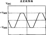
FCGCFlow to integrator (10).FCGC circuit 40 comprises that current source, electric capacity, inverter are to measure the interval of each Q and QN, if the interval of signal Q or QN surpasses predefined time window, in general 7.5ms, FCGC circuit will absorb the electric current of amplifier 10 or to amplifier 10 injection currents.When Q, QN surpass predefined time window, show that integrator 10 is saturated, it is maximum that output voltage reaches.Unless this situation is by very fast reparation, otherwise the hearer just can feel the artificial audio frequency relevant with the audio frequency output violent change.Fig. 2 B is a typical amplitude limit audio frequency output, the output V of the amplifier of prior art
OHCReaching maximum output V
MAXIn time, blocked.In order to prevent that amplitude limit and switching frequency are lower than 100KHZ, FCGC circuit 40 increases or reduces the electric current that enters integrator 10, so that the state of rapid conversion comparator 12.So, if the output of comparator 12 is Q, electric current will be increased so that comparator is switched to QN on the integrator 10.Equally, if the output of comparator 12 is QN or lower, reduce the electric current of integrator 10, so that comparator 12 is switched to Q or higher output rapidly.
At least 7.5ms is constant if the state of comparator keeps.Because integrator 10 is fast saturated, the amplitude limit output shown in Fig. 2 B will be produced probably.In order to prevent to produce amplitude limit, FCGC circuit 40 is to integrator 10 injections or therefrom extract one part of current, so that switch the state of comparator rapidly.So, if the output of comparator 12 is Q, electric current will be increased so that comparator is switched to QN on the integrator 10.Equally, if the output of comparator 12 is QN or lower, reduce the electric current on the integrator 10, so that comparator 12 is switched to Q or higher output rapidly.
FCGC circuit 40 changes the gain of amplifier 100 effectively by increasing or reducing the electric current that flows into integrator 10, and this phenomenon is called as gain compression.Caused being called as the correction output signal of soft limiting signal.Fig. 2 A is one and has vertical coordinate axle (V
OSC) typical soft limiting signal.When signal rises to maximum V
MAXThe time, output V
OSCCome to a point gradually, thisly come to a point far differently with hard-limiting shown in Fig. 2 B input waveform gradually, because gain has reduced, integrator 10 is saturated never.As further result, the sample frequency of amplifier 100 is also compensated to remain on the audio frequency automatically.For example, in an embodiment of the invention, amplifier 100 keeps sample frequency to be not less than 125KHZ for a maximum output of 100 watts nearly.The result is on the corresponding threshold value of time that FCGC circuit 40 is sampled, and amplifier 100 reduces gain continuously gradually, preventing output signal by hard-limiting, and the sample frequency of comparator is maintained on the frequency that is higher than input audio signal certainly.
Fig. 3 has shown the details of FCGC circuit 40, below with regard to electronic circuit 41, explains that comparator 12 has kept signal Q height at least after the 7.5ms, and how circuit will be operated.Those skilled in the art know that electronic circuit 42 is equal to electronic circuit 41 fully, and compensation QN.
Nmos pass transistor 412,414 provides a lasting current source, and this current source can constantly be sought chance and give capacitor C 1 discharge, and capacitor C 1 is shown typical 5 pf capacitance value.PMOS transistor 410 typically+7 volt with high voltage supply line V
DDConnect.The other end of transistor 410 is connected with capacitor C 1, the EN signal is added to transistor 416 has promptly started circuit 41.When Q reduced, PMOS transistor 410 was connected, and transistor 410 begins to capacitor C 1 charging, and the charging interval is by the relative size decision of transistor 410,412,414.Execution mode is to select 410,412,414 by size preferably, so as the electric capacity of capacitor C 1 to be equivalent on the time be the electric capacity of 7.5ms.When being full of soon, the threshold value of the inverter of being made up of transistor 420,422,424,426 is activated, and the inverter that is activated is connected PMOS transistor 430, therefore will export soft limiting signal V
SCHigh voltage supply line V with+7 volts
DDConnect.+ 7Volts is used for resistance R
FCGC,, so that increase the electric current of integrator 10.This will change the state of comparator 12.
When QN continues the low 7.5ms that reaches when above, electronic circuit 42 is carried out a kind of similar functions of switching comparator 12, and transistor 452,454 provides current source with to capacitor C 2 discharges; Transistor 452,454 1 ends are connected to low supply lines V with-7 volts
EE, the other end is connected to the end of capacitor C 2; Transistor 450 is at high supply lines V
DDBe connected between the capacitor C 2; Transistor 450,452,454 decision size like this: when 450 connect, charge C to C2 with 7.5ms nearly
2During charging, the threshold value of the inverter of being made up of C460, C462 is triggered, and connects transistor 470 like this and will export V
SCLow-voltage power supply line V with-7 volts
EConnect.
FET above the current detection circuit 110 comprises two resistance 111 and 112, (this is at my another common unsettled patent application Serial No.09/183/453 as a reference for 113,114 and current mirrors 115,116 of two PnP transistors, 1998/8/30 application has description among the Atty.Docket No.87552.98R256).Resistance 111 and 112 will convert the high voltage in the bridge 20 to corresponding electric current.For example, I
1=(+bus-Vbe)/R111; When top FET connects, I
1=(+bus-Vbe-Von)/R112.The wherein voltage drop that the pnp base-emitter is tied during Vbe, the pressure drop during Von on the MOSFET22.R111, R112 are respectively the resistance values of resistance 111,112.Current mirror, MOSFET115,116 is I relatively
1And I
2If I
2Greater than I
1, the T point voltage is just high so, otherwise just low.Resistance 112 is less than R111, like this under the normal operation, and when FET22 connects, I
2Compare I
1Big and A point voltage height.At the super-high-current time durations, the pressure drop Von between FET22 is very high, makes I
2Less than I
1And the T point voltage remains on low.The ratio of resistance R 111, R112 is provided with the overload current threshold value.In one embodiment, resistance 112 almost be R111 value 85%, and the R of FET
DSONBe 180mohms.
For making this circuit have the function of surveying overload current, need obturation.Under the normal operation, when just thinking the interior electric current of FET22 connection and FET22 less than the overload current threshold value, the T point voltage is high.Above the FET lock-out circuit allow FET22 to connect and before making any decision that relates to overload current, the rising of T point.Output signal T can compare with reference voltage-3.5V.Above FET when beginning to connect, the disabling pulse that has a 300ns begins, if before disabling pulse finishes, T point does not raise, the output of not gate 52 will reduce and the signal OC rising of top FET so.This will send out an overload current signal to FET22, and bridge can disconnect.Or take other measures to reduce electric current, this circuit advantage has been to remove the needs of giving the chip high voltage bus, in addition, can also protect the FET of above and below.
Those skilled in the art know that the FET lock-out circuit below corresponding low FET (not providing) on the current detection circuit and can provide the signal OC of the FET below the signal.
Overload current restriction (OCL) circuit 200 has transistor 213,212, inverter 15 and resistance R cl.As described above, the gain of modulator 100 is compressed by the electric current of the addition node of the integrator 10 of flowing through is controlled.OCL circuit 200 uses this technical limitations electric current.Audio signal is converted to electric current by Rin, is applied to the addition node of integrator then.By reducing to flow into or flow out the effective current realization gain compression of integrator addition node.Current limiting element 213,215,15 and Rcl can cooperate to reduce effective input current with any overload current detection circuit, have so just reduced Amplifier Gain and electric current.
OCL200 receives two logical signals, and one is the OC of top FET, and when having the overload current condition to exist in the top FET22, the OC of top FET is just high; Another is the OC of following FET, and when having the overload current condition to exist in the following FET24, the OC of following FET is just high.
When the overload current condition is arranged in the FET22, PMOS212 will connect and through R
C1Inject the electric current of the addition node that flows into integrator 10.FET22 above disconnecting during final result, the FET24 below connecting.This has just reduced the electric current in the FET22.With regard to amplifier 100, gain compression during final effect.Because top FET22 is short turn-on time, following FET is long turn-on time, and the gain of audio signal reduces.This technology can be adjusted the peak current in the MOSFET.When the overload current condition was arranged in the FET24, NMOS213 connected, and told the electric current of addition inter-node, and the FET24 below disconnecting, the FET22 above connecting, final result are the electric currents of the FET below having reduced.For audio frequency, gain has reduced.
Compare with existing interrupt circuit technology.OCL circuit 200 has significant advantage:
1.OCL circuit 200 is very fast.Feedback is digital, does not therefore need audio frequency output filtering, and seldom time-delay or not time-delay are arranged.Because just fed back before output filtering, filtering delay-time just is not a problem.If produce the OC electric current after low-pass filtering, this technology is with inoperative.Phase shift will cause positive feedback inevitably.
2.OCL circuit 200 is easy to stablize.Compare, it is stable through the intrinsic delay of the analog feedback loop of filtering system to be difficult to.
3.OCL circuit 200 reduces the gain of amplifier 100 gradually.Lead soft limiting and deleted the undesired artificial audio frequency that causes by hard-limiting.
4. the impedance of loud speaker 30 usually is lower than the DC rated value.Therefore the audio frequency amplifier that has the overload current latch circuit is easy to break down.Fault can not take place in current-limiting apparatus.
Fig. 4 has ignored detection circuit 100, is convenient to describe the operating process of Low ESR control LIC300 like this.By increasing quick pinning function, LIC300 has improved the circuit design of Fig. 1.Those skilled in the art know detection circuit 100 or another detection circuit, such as shown in Figure 5, provide the FET above the necessary logical signal OC and below the OC of FET necessary.In audio frequency amplifier, two kinds of situations of necessary differentiation impedance speakers and short circuit.The former also needs the electric current restriction, briefly, needs an overload current latch exactly.Otherwise amplifier will have to operate difficultly, avoid short circuit.This will cause too early failure and too much heating.Under the very low situation of impedance (less than nominal value 1/4), with regard to the necessary amplifier that disconnects immediately.Circuit among Fig. 4 detects duty ratio at the L point, is used for judging load impedance.When amplifier did not have current limliting, some L was ternary.Like this, just and closely the voltage between the integrator addition node of voltage is about the same for its voltage.
LIC control circuit 300 detects duty ratio at a L, and duty ratio and load current are proportional.Like this, it can be used for the measurement of load impedance.When being lower than acceptable limit value, amplifier disconnects immediately when impedance (being weighed by electric current).This quick overload electric current pins characteristic and ensures the incomplete short circuit of amplifier.
When in FET22 during by overload current, the pulse that some L initiates is from+7 to 0.Because need more gain compression to finish the electric current restriction, the duty factor of this pulse (duty cycle) increases along with the decline of load impedance.After a low pass filter 302, the analog signal of some M is admitted to the input of comparator 303 and 305.If this signal, means that amplifier 100 has slight load greater than 1V, the output of door 307 is lower, and PMOS312 is in on-state.Current source begins the charging of overtime (time out) capacitor, when voltage reaches 5V on the electric capacity, and upset comparator 315, overload circuit latch 320 is set up.Like this, during than underload, reach amplifier before latch is set up and disconnect one section time-out time before, amplifier must be in the electric current restriction state.If load impedance is very low, the M point voltage will be above 4V, upset comparator 305, and this can be provided with latch 320 immediately.
When in FET24 overload current being arranged, the pulse that some L initiates is from-7 to 0.Because need more gain compression to finish the electric current restriction, the duty factor of this pulse increases along with the decline of load impedance.After a low-pass filtering, the analog signal of some M is admitted to the input of comparator 304 and 306.If this signal means that less than-1V amplifier 100 loads are slight.Door 307 outputs are lower, and PMOS312 is in on-state.Current source begins to overtime capacitor charging, when voltage reaches 5V on the electric capacity, and upset comparator 315, the overload circuit latch is set up.Like this, during than underload, before the latch setting, amplifier must be in the electric current restriction state at time-out period.If load impedance is very low, the M point voltage will less than-4V and the comparator 306 that overturns, this can be provided with latch immediately, disconnects amplifier.
When being used to be provided with the threshold value that to detect low load impedance still be short circuit, the ratio of Rcl and Rin is very important.If the current value that Rcl is chosen as in the maximal audio input signal it is greater than Rin, like this, the quick overload electric current pins and will participate in into never, because the duty factor that L is ordered can limit electric current.Amplifier will always enter electric current restriction, and at this moment people are reluctant to see, because maximum output current will be admitted to short-circuit condition.The high electric current that can not provide Rin to provide is provided Rcl.Under this mode, the duty factor that L is ordered will increase sharply along with the reduction of load impedance, can earlier excite the quick overload electric current to pin.
OCL200 receives two logical signals, and one is the OC of top FET.When the overload current condition exists in FET22, the OC height of top FET; Another is the OC of following FET, when the overload current condition exists in FET22, and the OC height of following FET.When among the FET22 overload current being arranged, PMOS212 connect and by Rcl to integrator 10 injection currents.Disconnect FET22 during its net result, the FET24 below connecting.This can reduce the electric current among the FET22.With regard to amplifier 100, final result is a gain compression.Because FET22 is few when connecting, following FET24 is many when connecting, and the audio signal gain reduces.When the overload current condition was arranged among the FET24, NMOS213 connected and extracts from the addition node.FET24 below disconnecting, the FET22 above connecting.Electric current among the FET24 below its result has reduced.Under the situation of audio frequency, gain reduces.
Claims (10)
1, comprises the D class A amplifier A of a bridge circuit, an overload current restricting circuits of forming by a self-oscillation pulse width modulator and a comparator that is connected with integrator output, the self-oscillation pulse width modulator comprises an integrator with feedback, feedback is from the output of amplifier, a portal drive circuit that between modulator and MOSFET bridge circuit, is connected, the MOSFET bridge circuit is used for the bridge at bridge circuit control MOSFET, is characterised in that: bridge circuit is connected between the high low voltage lines and is made up of two MOSFET that connect that are one another in series at least; Load impedance links to each other with the output of bridge circuit; In two MOSFET, detect the device of overload current; The overload current restraint device is used for detecting the overload current of MOSFET, and reduces Amplifier Gain when detecting current overload, thereby reduces output current, reduces to the predefine value up to peak current.
2, D class A amplifier A as claimed in claim 1, feature is that also the overload current restraint device is made up of one or more current sources, current source can increase or shunt the electric current of integrator, with the electric current of any MOSFET of box lunch during greater than the threshold value of electric current restriction, reduce effective input current of integrator, current source is made up of a pair of transistor that is connected with a resistance, resistance is connected with the integrator of D class A amplifier A, logical circuit is connected with transistorized control end, can select a transistor to increase electric current or extract stream out to integrator like this.
3, D class A amplifier A as claimed in claim 2, feature is that also logic device is made up of two devices, the first detects the device of electric current in the bridge circuit, it two is that detected electric current is compared with a reference value, thereby produce the logical signal of expression current overload, comprise a Low ESR testing circuit, be used for detecting the duty factor of resistance and transistor junction, and produce the signal of an expression load impedance.
4, the D class A amplifier A described in claim 3, feature is that also the Low ESR transistor is by a low pass filter, four comparators, each comparator is all by different reference values, be used for distinguishing the short circuit current that hangs down load and short circuit and when short circuit, disconnect amplifier immediately, the overtime electric capacity that is connected with load detecting resistance, it is certain that it fills for before disconnecting amplifier overtime electric capacity.
5, D class A amplifier A as claimed in claim 2, feature are that also the overload current restraint device is connected with power supply by an end, and the other end is connected with integrator with the transistor of a control end that is connected with this device and forms, and is used for detecting the overload current among the MOSFET.
6, D class A amplifier A as claimed in claim 2, feature also is to provide positive-negative power, and the overload current restraint device is made up of two transistors, and first transistor AND gate positive supply connects, and positive supply provides a control end to be connected with a MOSFET; Second transistor AND gate negative supply connects, and negative supply provides a control end to be connected with another MOSFET.
7, D class A amplifier A as claimed in claim 1, feature also is to be used to detect the device of the voltage drop on the MOSFET and is made up of two change-over circuits, first change-over circuit converts the voltage drop on the MOSFET to represent the voltage on the MOSFET current signal, so this change-over circuit has the current output signal of an expression voltage; Second change-over circuit converts the voltage drop that at least two MOSFET go up another to represent the voltage drop on another MOSFET current signal, and described second change-over circuit has the output signal of the electric current of representing described another MOSFET of flow path.
8, D class A amplifier A as claimed in claim 1, feature is that also the low impedance current restraint device is connected with the overload current restraint device, when load is lower than first threshold value, gate driver forbids that rapidly the door of MOSFET drives, here, the low impedance current restraint device comprises time-delay mechanism, and the driving that is used for this door to MOSFET remains to after one section time-delay after load drops to second threshold value, and time-delay is by the time-delay mechanism setting.
9, D class A amplifier A as claimed in claim 8, feature is that also the overload current restraint device produces an overload current restricting signal, the low impedance current restraint device comprises a low pass filter, on behalf of the amplitude of load, low pass filter convert the overload current restricting signal to the low impedance current restricting signal by one, when exceeding first impedance threshold, signal is sent to the driver of MOSFET.
10, D class A amplifier A described in claim 8, wherein the low impedance current restraint device comprises a low pass filter that is connected with OCL200, a plurality of comparators that connect with low pass filter and different reference threshold, a latch, be used for when surpassing first load impedance threshold value, stop the operation of the gate driver of MOSFET rapidly, this latch comprises the electric capacity that a current source and one are connected between comparator and latch, when load impedance surpasses second threshold value, this electric capacity latch delay operation a period of time, time of delay is by the electric capacity setting.
Applications Claiming Priority (2)
| Application Number | Priority Date | Filing Date | Title |
|---|---|---|---|
| US10894298P | 1998-11-18 | 1998-11-18 | |
| US60/108,942 | 1998-11-18 |
Publications (1)
| Publication Number | Publication Date |
|---|---|
| CN1255779A true CN1255779A (en) | 2000-06-07 |
Family
ID=22324944
Family Applications (1)
| Application Number | Title | Priority Date | Filing Date |
|---|---|---|---|
| CN99124444A Pending CN1255779A (en) | 1998-11-18 | 1999-11-18 | D-modulator with peak value current limit and loaded impedance detection circuit |
Country Status (5)
| Country | Link |
|---|---|
| US (1) | US6229389B1 (en) |
| EP (1) | EP1003280A2 (en) |
| JP (1) | JP2000165154A (en) |
| CN (1) | CN1255779A (en) |
| TW (1) | TW421909B (en) |
Cited By (8)
| Publication number | Priority date | Publication date | Assignee | Title |
|---|---|---|---|---|
| CN100405714C (en) * | 2003-12-16 | 2008-07-23 | 英特赛尔美国股份有限公司 | System and method of detecting phase body diode using a comparator in a synchronous rectified fet driver |
| CN100433547C (en) * | 2002-05-13 | 2008-11-12 | 索尼株式会社 | Power amplification device |
| CN103227614A (en) * | 2012-01-26 | 2013-07-31 | 株式会社东芝 | Power amplifying apparatus and audio system |
| CN104079244A (en) * | 2013-03-29 | 2014-10-01 | 茂达电子股份有限公司 | Output stage circuit, overcurrent protection method thereof and audio amplification system |
| CN104617897A (en) * | 2015-03-03 | 2015-05-13 | 深圳市芯电威科技有限公司 | Audio power amplifier circuit |
| CN107168437A (en) * | 2017-07-04 | 2017-09-15 | 中国科学技术大学 | A kind of bipolar current source |
| CN108574462A (en) * | 2018-01-31 | 2018-09-25 | 中兴通讯股份有限公司 | Protect circuit, circuit protection method |
| CN111541975A (en) * | 2020-04-27 | 2020-08-14 | 维沃移动通信有限公司 | Audio signal adjusting method and electronic equipment |
Families Citing this family (46)
| Publication number | Priority date | Publication date | Assignee | Title |
|---|---|---|---|---|
| US6833757B2 (en) * | 1999-12-15 | 2004-12-21 | Texas Instruments Incorporated | Method and system for improving amplifier efficiency |
| EP1118865A1 (en) * | 2000-01-20 | 2001-07-25 | STMicroelectronics S.r.l. | Circuit and method for detecting load impedance |
| FR2812478B1 (en) * | 2000-07-27 | 2003-01-10 | Rene Lambruschi | ELECTRONIC CIRCUIT FOR CONVERTING A SIGNAL AND AMPLIFIER INCORPORATING SAID CIRCUIT |
| JP2002299968A (en) * | 2001-03-30 | 2002-10-11 | Pioneer Electronic Corp | D-class amplifier |
| JP5114818B2 (en) * | 2001-08-13 | 2013-01-09 | ヤマハ株式会社 | Current detection method, current detection circuit and overcurrent protection circuit |
| US20040139799A1 (en) * | 2002-07-25 | 2004-07-22 | Sudolcan David C. | Method and apparatus for determining flow rate of a fluid |
| JP2004122300A (en) * | 2002-10-03 | 2004-04-22 | Tenryu Saw Mfg Co Ltd | Rotating saw |
| KR20040038174A (en) * | 2002-10-31 | 2004-05-08 | 주식회사 디엠비테크놀로지 | Digital audio amplifier capable of increasing self-oscillation frequency and reducing the number of component |
| WO2004082133A1 (en) * | 2003-03-10 | 2004-09-23 | Koninklijke Philips Electronics N.V. | Three state class d amplifier |
| JP4620043B2 (en) * | 2003-03-21 | 2011-01-26 | ディー2オーディオ コーポレイション | Acoustic amplifier circuit protection system and method |
| US7929718B1 (en) | 2003-05-12 | 2011-04-19 | D2Audio Corporation | Systems and methods for switching and mixing signals in a multi-channel amplifier |
| JP3863133B2 (en) * | 2003-09-25 | 2006-12-27 | 沖電気工業株式会社 | Signal amplification circuit |
| KR100609266B1 (en) | 2003-11-03 | 2006-08-04 | 삼성전자주식회사 | Method of detecting fault and circuit for performing the same, method of protecting circuit of a power amp in accordance with the fault and power amp for detecting the fault |
| US20060043948A1 (en) * | 2004-08-30 | 2006-03-02 | Xuening Li | Load transient frequency modulation in fixed frequency PWM regulator |
| US20060043949A1 (en) * | 2004-08-30 | 2006-03-02 | Xuening Li | Load transient frequency modulation in fixed frequency PWM regulator |
| WO2005096777A2 (en) * | 2004-04-02 | 2005-10-20 | Texas Instruments Incorporated | Load transient frequency modulation in fixed frequency pwm regulator |
| SI21892A (en) * | 2004-09-29 | 2006-04-30 | Vinko Kunc | Procedure and circuit for measuring extremely low electric currents |
| US7259618B2 (en) * | 2005-08-25 | 2007-08-21 | D2Audio Corporation | Systems and methods for load detection and correction in a digital amplifier |
| EP1770855B1 (en) * | 2005-09-28 | 2011-08-17 | Yamaha Corporation | Class D amplifier |
| US20070139109A1 (en) * | 2005-12-21 | 2007-06-21 | Jun Honda | Class d amplifier with start-up click noise elimination |
| US7286010B2 (en) * | 2006-01-26 | 2007-10-23 | D2Audio Corporation | Systems and methods for over-current protection |
| JP4759050B2 (en) * | 2006-05-15 | 2011-08-31 | 旭化成エレクトロニクス株式会社 | Drive device |
| CN101443999B (en) * | 2006-05-15 | 2012-07-25 | 旭化成电子材料元件株式会社 | Drive device, drive method, and information device |
| KR20070113434A (en) * | 2006-05-23 | 2007-11-29 | 삼성전자주식회사 | Automatic input-gain control circuit, and method thereof |
| EP2041866B1 (en) * | 2006-07-07 | 2018-12-26 | Nxp B.V. | Class d audio amplifier |
| CN101267100B (en) * | 2008-01-15 | 2012-12-26 | 深圳创维-Rgb电子有限公司 | Exception protection device for negative and positive dual power supply circuit |
| US7994819B2 (en) * | 2008-02-12 | 2011-08-09 | Texas Instruments Incorporated | Level-shifter circuit |
| JP5266830B2 (en) * | 2008-03-26 | 2013-08-21 | ヤマハ株式会社 | Self-excited class D amplifier |
| DE102008027765B3 (en) | 2008-06-11 | 2010-05-12 | Austriamicrosystems Ag | Amplifier arrangement and method for signal amplification |
| KR100979377B1 (en) * | 2008-07-28 | 2010-08-31 | 진옥상 | Excess current limitation circuit |
| TWI413359B (en) * | 2009-07-24 | 2013-10-21 | Wistron Corp | High efficiency audio amplifier and method thereof |
| TWI380580B (en) * | 2009-08-20 | 2012-12-21 | Richtek Technology Corp | Variable frequency class-d amplifier and a control method thereof and a ramp generator for the variable freguency class-d amplifier and a method thereof |
| US8581659B2 (en) * | 2010-01-25 | 2013-11-12 | Dongbu Hitek Co., Ltd. | Current controlled current source, and methods of controlling a current source and/or regulating a circuit |
| US8497734B2 (en) | 2010-06-14 | 2013-07-30 | Harman International Industries, Incorporated | High efficiency audio amplifier system |
| US8482346B2 (en) * | 2010-06-14 | 2013-07-09 | Harman International Industries, Incorporated | High efficiency balanced output amplifier system |
| CN102984629B (en) * | 2011-09-06 | 2014-12-17 | 昂宝电子(上海)有限公司 | Method used for reducing noise in voice frequency amplification system |
| CN102984630B (en) | 2011-09-06 | 2015-12-02 | 昂宝电子(上海)有限公司 | For reducing the system and method for distortion in audio amplifier system |
| TWI482505B (en) * | 2012-09-19 | 2015-04-21 | Wistron Corp | Speaker control system |
| DE102013207898A1 (en) * | 2013-04-30 | 2014-10-30 | Novero Dabendorf Gmbh | Compensation of signal attenuation in the transmission of transmission signals of a mobile device |
| CN103441739B (en) | 2013-08-21 | 2015-04-22 | 昂宝电子(上海)有限公司 | Amplification system with one or more channels and amplification method |
| US9685919B2 (en) | 2013-08-21 | 2017-06-20 | On-Bright Electronics (Shanghai) Co., Ltd. | Amplification systems and methods with output regulation |
| KR101855725B1 (en) | 2014-01-13 | 2018-06-20 | 삼성전자주식회사 | Audio Outputting Control Method and Electronic Device supporting the same |
| CN105450186B (en) | 2014-08-29 | 2019-04-19 | 意法半导体研发(深圳)有限公司 | High level current limitation function for audio-frequency amplifier |
| US10663531B2 (en) * | 2017-10-11 | 2020-05-26 | Cirrus Logic, Inc. | Digital short detection method of class D amplifier |
| US10230414B1 (en) | 2018-06-08 | 2019-03-12 | Motorola Solutions, Inc. | Method and apparatus to reduce communication device peak current |
| US10703270B1 (en) * | 2018-07-10 | 2020-07-07 | SBS, Incorporated | Parking brake alarm systems with driver absence detection |
Family Cites Families (4)
| Publication number | Priority date | Publication date | Assignee | Title |
|---|---|---|---|---|
| US5805020A (en) * | 1996-06-27 | 1998-09-08 | Harris Corporation | Silent start class D amplifier |
| US6016075A (en) * | 1997-06-04 | 2000-01-18 | Lord Corporation | Class-D amplifier input structure |
| US6107875A (en) * | 1998-10-15 | 2000-08-22 | Intersil Corporation | Variable frequency class D modulator with built in soft clipping and frequency limiting |
| US6108182A (en) * | 1998-10-30 | 2000-08-22 | Intersil Corporation | Overcurrent sensing circuit and self adjusting blanking |
-
1999
- 1999-11-12 US US09/438,210 patent/US6229389B1/en not_active Expired - Fee Related
- 1999-11-17 EP EP99402849A patent/EP1003280A2/en not_active Withdrawn
- 1999-11-18 CN CN99124444A patent/CN1255779A/en active Pending
- 1999-11-18 TW TW088120152A patent/TW421909B/en active
- 1999-11-18 JP JP11328483A patent/JP2000165154A/en active Pending
Cited By (13)
| Publication number | Priority date | Publication date | Assignee | Title |
|---|---|---|---|---|
| CN100433547C (en) * | 2002-05-13 | 2008-11-12 | 索尼株式会社 | Power amplification device |
| CN100405714C (en) * | 2003-12-16 | 2008-07-23 | 英特赛尔美国股份有限公司 | System and method of detecting phase body diode using a comparator in a synchronous rectified fet driver |
| CN103227614B (en) * | 2012-01-26 | 2016-03-16 | 株式会社东芝 | Power amplification device and audio system |
| CN103227614A (en) * | 2012-01-26 | 2013-07-31 | 株式会社东芝 | Power amplifying apparatus and audio system |
| CN104079244B (en) * | 2013-03-29 | 2016-12-28 | 茂达电子股份有限公司 | Output stage circuit, overcurrent protection method thereof and audio amplification system |
| CN104079244A (en) * | 2013-03-29 | 2014-10-01 | 茂达电子股份有限公司 | Output stage circuit, overcurrent protection method thereof and audio amplification system |
| CN104617897A (en) * | 2015-03-03 | 2015-05-13 | 深圳市芯电威科技有限公司 | Audio power amplifier circuit |
| CN104617897B (en) * | 2015-03-03 | 2018-08-28 | 广东芯威电声技术有限公司 | A kind of audio power amplifier circuit |
| CN107168437A (en) * | 2017-07-04 | 2017-09-15 | 中国科学技术大学 | A kind of bipolar current source |
| CN107168437B (en) * | 2017-07-04 | 2019-06-11 | 中国科学技术大学 | A kind of bipolar current source |
| CN108574462A (en) * | 2018-01-31 | 2018-09-25 | 中兴通讯股份有限公司 | Protect circuit, circuit protection method |
| CN108574462B (en) * | 2018-01-31 | 2021-03-26 | 中兴通讯股份有限公司 | Protection circuit and circuit protection method |
| CN111541975A (en) * | 2020-04-27 | 2020-08-14 | 维沃移动通信有限公司 | Audio signal adjusting method and electronic equipment |
Also Published As
| Publication number | Publication date |
|---|---|
| US6229389B1 (en) | 2001-05-08 |
| JP2000165154A (en) | 2000-06-16 |
| EP1003280A2 (en) | 2000-05-24 |
| TW421909B (en) | 2001-02-11 |
Similar Documents
| Publication | Publication Date | Title |
|---|---|---|
| CN1255779A (en) | D-modulator with peak value current limit and loaded impedance detection circuit | |
| US6160388A (en) | Sensing of current in a synchronous-buck power stage | |
| US7701287B2 (en) | Voltage detection type overcurrent protection device for class-D amplifier | |
| CN102160271B (en) | Control method for power control circuit, power supply unit, power supply system, and power controller control method | |
| JP3684461B2 (en) | Pulse width modulation controller for resonant converter | |
| US6815937B2 (en) | Stepping inductor for fast transient response of switching converter | |
| CN1257343A (en) | Low-noise and low distortion D type amplifier | |
| US20040135559A1 (en) | DC to DC converter producing output voltage exhibit rise and fall charactristics independet of load thereon | |
| CN102957383B (en) | Class-D amplifier and control method | |
| CN106469994B (en) | Electric power converter and MRI system including this converter | |
| CN104201883A (en) | Control circuit for switching converter | |
| CN104065266A (en) | Control circuit for voltage converter | |
| CN101689803A (en) | Power supply device | |
| JP2003511005A (en) | Pulse width modulated bridge circuit in a second bridge circuit | |
| US6348783B2 (en) | DC/DC converter for suppressing effects of spike noise | |
| US20040178777A1 (en) | Method of forming a power system and structure therefor | |
| CN113098267B (en) | Switch converter, switch integrated circuit and control circuit thereof | |
| US20070085522A1 (en) | Control device for switching converter and switching converter incorporating same | |
| CN109756116A (en) | Boost chip and its short-circuit protection circuit | |
| US6229339B1 (en) | Circuit for driving switching element | |
| CN204376704U (en) | Control circuit for voltage converter | |
| CN204013219U (en) | Control circuit for switching converter | |
| CN2765408Y (en) | Ring current signal generating circuit | |
| CN102082509B (en) | Frequency control circuit and method for inverter voltage regulator | |
| US7586760B2 (en) | Snubber capacitor resetting in a DC-to-DC converter |
Legal Events
| Date | Code | Title | Description |
|---|---|---|---|
| C06 | Publication | ||
| PB01 | Publication | ||
| C02 | Deemed withdrawal of patent application after publication (patent law 2001) | ||
| WD01 | Invention patent application deemed withdrawn after publication |