CN1244154C - Semiconductor storaging device - Google Patents
Semiconductor storaging device Download PDFInfo
- Publication number
- CN1244154C CN1244154C CNB011439599A CN01143959A CN1244154C CN 1244154 C CN1244154 C CN 1244154C CN B011439599 A CNB011439599 A CN B011439599A CN 01143959 A CN01143959 A CN 01143959A CN 1244154 C CN1244154 C CN 1244154C
- Authority
- CN
- China
- Prior art keywords
- mentioned
- semiconductor storage
- magnetic element
- word line
- transistor
- Prior art date
- Legal status (The legal status is an assumption and is not a legal conclusion. Google has not performed a legal analysis and makes no representation as to the accuracy of the status listed.)
- Expired - Fee Related
Links
- 239000004065 semiconductor Substances 0.000 title claims abstract description 59
- 230000005291 magnetic effect Effects 0.000 claims description 85
- 230000015572 biosynthetic process Effects 0.000 claims description 6
- 239000004020 conductor Substances 0.000 claims description 3
- 239000010410 layer Substances 0.000 description 100
- 230000005294 ferromagnetic effect Effects 0.000 description 30
- 230000005415 magnetization Effects 0.000 description 27
- 239000012790 adhesive layer Substances 0.000 description 20
- 230000008676 import Effects 0.000 description 17
- 238000010586 diagram Methods 0.000 description 14
- 230000000694 effects Effects 0.000 description 10
- 238000003475 lamination Methods 0.000 description 9
- 230000005303 antiferromagnetism Effects 0.000 description 8
- 239000000758 substrate Substances 0.000 description 8
- 230000008859 change Effects 0.000 description 4
- 239000000463 material Substances 0.000 description 4
- 230000002093 peripheral effect Effects 0.000 description 4
- 230000009471 action Effects 0.000 description 3
- 238000000034 method Methods 0.000 description 3
- 230000005641 tunneling Effects 0.000 description 3
- IJGRMHOSHXDMSA-UHFFFAOYSA-N Atomic nitrogen Chemical compound N#N IJGRMHOSHXDMSA-UHFFFAOYSA-N 0.000 description 2
- 238000003491 array Methods 0.000 description 2
- 239000003989 dielectric material Substances 0.000 description 2
- 230000005307 ferromagnetism Effects 0.000 description 2
- 229910052748 manganese Inorganic materials 0.000 description 2
- 230000004048 modification Effects 0.000 description 2
- 238000012986 modification Methods 0.000 description 2
- 229910052757 nitrogen Inorganic materials 0.000 description 2
- 229910052760 oxygen Inorganic materials 0.000 description 2
- 230000008569 process Effects 0.000 description 2
- 229910000967 As alloy Inorganic materials 0.000 description 1
- 229910004261 CaF 2 Inorganic materials 0.000 description 1
- 229910002551 Fe-Mn Inorganic materials 0.000 description 1
- YCKRFDGAMUMZLT-UHFFFAOYSA-N Fluorine atom Chemical compound [F] YCKRFDGAMUMZLT-UHFFFAOYSA-N 0.000 description 1
- 229910003286 Ni-Mn Inorganic materials 0.000 description 1
- 229910005811 NiMnSb Inorganic materials 0.000 description 1
- 229910004298 SiO 2 Inorganic materials 0.000 description 1
- 229910002367 SrTiO Inorganic materials 0.000 description 1
- 238000009825 accumulation Methods 0.000 description 1
- 229910045601 alloy Inorganic materials 0.000 description 1
- 239000000956 alloy Substances 0.000 description 1
- 229910052782 aluminium Inorganic materials 0.000 description 1
- QVGXLLKOCUKJST-UHFFFAOYSA-N atomic oxygen Chemical group [O] QVGXLLKOCUKJST-UHFFFAOYSA-N 0.000 description 1
- 229910052796 boron Inorganic materials 0.000 description 1
- 229910052799 carbon Inorganic materials 0.000 description 1
- 238000010276 construction Methods 0.000 description 1
- 229910052802 copper Inorganic materials 0.000 description 1
- 230000006866 deterioration Effects 0.000 description 1
- 238000005516 engineering process Methods 0.000 description 1
- 230000002349 favourable effect Effects 0.000 description 1
- 229910052731 fluorine Inorganic materials 0.000 description 1
- 239000011737 fluorine Substances 0.000 description 1
- 238000007429 general method Methods 0.000 description 1
- 229910052737 gold Inorganic materials 0.000 description 1
- 229910052741 iridium Inorganic materials 0.000 description 1
- 229910052742 iron Inorganic materials 0.000 description 1
- SZVJSHCCFOBDDC-UHFFFAOYSA-N iron(II,III) oxide Inorganic materials O=[Fe]O[Fe]O[Fe]=O SZVJSHCCFOBDDC-UHFFFAOYSA-N 0.000 description 1
- 229910052749 magnesium Inorganic materials 0.000 description 1
- 229910052750 molybdenum Inorganic materials 0.000 description 1
- 229910052759 nickel Inorganic materials 0.000 description 1
- 239000001301 oxygen Substances 0.000 description 1
- 229910052763 palladium Inorganic materials 0.000 description 1
- 229910052697 platinum Inorganic materials 0.000 description 1
- 229910052710 silicon Inorganic materials 0.000 description 1
- 229910052709 silver Inorganic materials 0.000 description 1
- 229910052721 tungsten Inorganic materials 0.000 description 1
- 229910052726 zirconium Inorganic materials 0.000 description 1
Images


Classifications
-
- H—ELECTRICITY
- H01—ELECTRIC ELEMENTS
- H01L—SEMICONDUCTOR DEVICES NOT COVERED BY CLASS H10
- H01L27/00—Devices consisting of a plurality of semiconductor or other solid-state components formed in or on a common substrate
- H01L27/02—Devices consisting of a plurality of semiconductor or other solid-state components formed in or on a common substrate including semiconductor components specially adapted for rectifying, oscillating, amplifying or switching and having at least one potential-jump barrier or surface barrier; including integrated passive circuit elements with at least one potential-jump barrier or surface barrier
- H01L27/04—Devices consisting of a plurality of semiconductor or other solid-state components formed in or on a common substrate including semiconductor components specially adapted for rectifying, oscillating, amplifying or switching and having at least one potential-jump barrier or surface barrier; including integrated passive circuit elements with at least one potential-jump barrier or surface barrier the substrate being a semiconductor body
- H01L27/10—Devices consisting of a plurality of semiconductor or other solid-state components formed in or on a common substrate including semiconductor components specially adapted for rectifying, oscillating, amplifying or switching and having at least one potential-jump barrier or surface barrier; including integrated passive circuit elements with at least one potential-jump barrier or surface barrier the substrate being a semiconductor body including a plurality of individual components in a repetitive configuration
-
- G—PHYSICS
- G11—INFORMATION STORAGE
- G11C—STATIC STORES
- G11C5/00—Details of stores covered by group G11C11/00
- G11C5/06—Arrangements for interconnecting storage elements electrically, e.g. by wiring
- G11C5/063—Voltage and signal distribution in integrated semi-conductor memory access lines, e.g. word-line, bit-line, cross-over resistance, propagation delay
-
- G—PHYSICS
- G11—INFORMATION STORAGE
- G11C—STATIC STORES
- G11C11/00—Digital stores characterised by the use of particular electric or magnetic storage elements; Storage elements therefor
- G11C11/02—Digital stores characterised by the use of particular electric or magnetic storage elements; Storage elements therefor using magnetic elements
- G11C11/14—Digital stores characterised by the use of particular electric or magnetic storage elements; Storage elements therefor using magnetic elements using thin-film elements
- G11C11/15—Digital stores characterised by the use of particular electric or magnetic storage elements; Storage elements therefor using magnetic elements using thin-film elements using multiple magnetic layers
Abstract
A semiconductor memory device includes a plurality of first wirings extending in a first direction, a plurality of memory elements connected with the first wirings, a plurality of second wirings extending in a second direction different from the first direction, the second wirings being disposed opposite to the first wirings with the memory elements interposed between the first and second wirings, the second wirings being spaced from the memory elements, and first transistors or diodes connected between two adjacent of the second wirings.
Description
Technical field
The present invention relates to semiconductor storage, particularly relate to tunnel magnetoresistive (TMR:Tunneling Magneto Resistive) element as the magnetic memory apparatus of memory element (MRAM: MAGNETIC RANDOM ACCESS MEMORY) write distribution.
Background technology
In recent years, as information storage elements, proposed to utilize the scheme of MRAM (Magnetic Random AccessMemory, the MAGNETIC RANDOM ACCESS MEMORY) memory cell of tunnel magnetoresistive (Tunneling MagnetoResistive :) effect hereinafter referred to as TMR.This mram memory cell, for example, by ISSCC2000 Technical Digest p.128 " A 10ns Read and WriteNon-Volatile Memory Array Using a Magnetic Tunnel Junction and FETSwitch in each Cell ", Roy Scheuerlein et.al has done announcement.
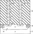
Figure 17 represents the equivalent circuit diagram of the semiconductor storage of prior art.Figure 18 represents the summary sectional view of TMR element.
As shown in figure 18, bit line 21 and word line 19,26 dispose mutually orthogonally, and TMR element 20 is configured in these line neutrality lines 21 and writes on the intersection point of word line 19.One end of this TMR element 20 is connected with bit line 21, and the other end is connected with transistor 13.And the grid of this transistor 13 becomes sense word line 26.
Above-mentioned TMR element 20 has by 2 magnetospheres and 3 layers of structure being formed by the nonmagnetic layer of these magnetosphere clampings.Promptly, as shown in figure 18, TMR element 20 is by the magnetization adhesive layer 41 that is connected with lower electrode 17, the magnetic recording layer 43 that is connected with bit line 21 by upper electrode (not drawing among the figure) and constituted by thin tunnel junction layers 42 of these magnetization adhesive layers 41 and magnetic recording layer 43 clampings.
Here, magnetization adhesive layer 41 is made of antiferromagnetism layer and ferromagnetic layer whose, is called to be used for the fixing pinning layer in one direction of magnetization.On the other hand, magnetic recording layer 43 is made of ferromagnetic layer whose, is called the accumulation layer that is used to store the free change information of the direction of magnetization.The direction of magnetization of this magnetic recording layer 43 can change according to electric current that flows through bit line 21 and the electric current formed resultant magnetic field of flowing through word line 19.
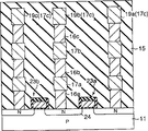
Figure 19 represents the sectional view of the semiconductor storage of prior art.As shown in figure 19, for example in P type semiconductor substrate (or trap) 11, selectively form STI (Shallow TrenchIsolation, shallow isolating trough) Gou Zao element separated region 12, on Semiconductor substrate 11, selectively form MOSFET13, below two ends of this MOSFET13, for example form the regions and source 14 of N type.Here, the grid of MOSFET13 becomes sense word line 26.Again, the 1st contact 16a that will be connected with regions and source 14 on Semiconductor substrate 11 is arranged in the dielectric film 15, on this 1st contact 16a the 1st distribution 17a is set.Equally, in dielectric film 15, the 2nd to the 4th contact 16b is set, 16c, 16d and the 2nd to the 4th distribution 17b, 17c, 17d.Here, the part of the 1st distribution 17a becomes Gnd (ground connection) line 18.Again, the part of the 3rd distribution 17c becomes and writes word line 19a, 19b, 19c.And TMR element 20 is connected with the 4th distribution 17d, and bit line 21 is connected with this TMR element 20.
Below, we illustrate simply that the data in the semiconductor storage of prior art write and read action.
At first,, during " 0 " information, select a pair of word line 19 and the bit line 21 of writing when on TMR element 20, writing " 1 " and since this select write word line 19 and bit line 21 both upper reaches overcurrent produce current field respectively.Therefore, magnetic field is with to be positioned at the selected cell that writes on word line 19 and bit line 21 intersection points relevant, because this magnetic field, TMR element 20 surpasses the magnetization inversion threshold value, can writing information.
At this moment, for example, when the direction of magnetization of magnetization adhesive layer 41 and magnetic recording layer 43 becomes when parallel, the tunnel resistor that goes out by the current detecting that flows in tunnel junction layer 42 reaches minimum, can store " 1 " at this state.On the other hand, when the direction of magnetization of magnetization adhesive layer 41 and magnetic recording layer 43 became antiparallel, the tunnel resistor that goes out by the current detecting that flows in tunnel junction layer 42 reached peak, can store " 0 " at this state.That is, in MRAM, as " 1 ", " 0 " information stores is got up with this tunnel resistor difference.
On the other hand, when reading " 1 " that writes TMR element 20, during " 0 " information, when selecting sense word line 26 and bit line 21, electric current by TMR element 20 and MOSFET13 from bit line 21 to flowing to Gnd line 18.And the difference of tunnel resistor that reads 20 of different TMR elements by peripheral circuits is carried out " 1 ", the judgement of " 0 " information as information.
But in the semiconductor storage of prior art, along with the progress of miniaturization, the distance between the unit shortens.That is, as shown in figure 19, the distance X that writes between word line of adjacency becomes below the 0.1 μ m.So, when writing data, for example, when in writing word line 19b, flowing through electric current, write word line 19a, 19c by what flow through that magnetic field that this electric current that writes word line 19b produces arrives adjacency.Therefore, adjacency write word line 19a, 19c is subjected to the influence of reverse current, occurs in the cross-interference issue that produces misoperation in the adjacent unit.
Summary of the invention
The semiconductor storage of the 1st viewpoint according to the present invention, it possesses the upwardly extending multiple bit lines the 1st side, the a plurality of magnetic elements that are connected with above-mentioned bit line, upwardly extending 2nd side different with above-mentioned the 1st direction, clip above-mentioned magnetic element from the two opposite sides of above-mentioned magnetic element together with above-mentioned bit line, and many word lines that dispose separatedly with above-mentioned magnetic element, the 1st transistor or the 1st diode that is connected with the above-mentioned word line of adjacency respectively, above-mentioned the 1st transistor or above-mentioned the 1st diode arrangement are in the outside in the memory cell array zone that has disposed above-mentioned magnetic element.
The semiconductor storage of the 2nd viewpoint according to the present invention, it possesses the upwardly extending multiple bit lines the 1st side, the a plurality of magnetic elements that are connected with above-mentioned bit line, upwardly extending 2nd side different with above-mentioned the 1st direction, clip above-mentioned magnetic element from the two opposite sides of above-mentioned magnetic element together with above-mentioned bit line, and many word lines that dispose separatedly with above-mentioned magnetic element, the 2nd transistor or the 2nd diode that is connected with the above-mentioned bit line of adjacency respectively, above-mentioned the 2nd transistor or above-mentioned the 2nd diode arrangement are in the outside in the memory cell array zone that has disposed above-mentioned magnetic element.
Description of drawings
Fig. 1 is the circuit diagram of the expression semiconductor storage relevant with the present invention's the 1st example.
Fig. 2 is the sectional view that is illustrated in the semiconductor storage in the a-quadrant shown in Figure 1.
Fig. 3 is the sectional view that is illustrated in the semiconductor storage in the B zone shown in Figure 1.
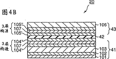
Fig. 4 A, 4B are the sectional views of the TMR element of the expression 1 heavy tunnel junction structure relevant with each example of the present invention.
Fig. 5 A, 5B are the sectional views of the TMR element of the expression 2 heavy tunnel junction structures relevant with each example of the present invention.
Fig. 6 is the figure that concerns between distance between word line and the current field that writes of expression adjacency.
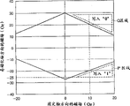
Fig. 7 is the figure of the star-like curve of expression TMR element.
Fig. 8 is the circuit diagram of expression other semiconductor storage relevant with the present invention's the 1st example.
Fig. 9 is the circuit diagram of the expression semiconductor storage relevant with the present invention's the 2nd example.
Figure 10 is the sectional view that is illustrated in the semiconductor storage in the C zone shown in Figure 9.
Figure 11 is the circuit diagram of expression other semiconductor storage relevant with the present invention's the 2nd example.
Figure 12 is the circuit diagram of the expression semiconductor storage relevant with the present invention's the 3rd example.
Figure 13 is the sectional view that is illustrated in the semiconductor storage in the D zone shown in Figure 12.
Figure 14 is the circuit diagram of expression other semiconductor storage relevant with the present invention's the 3rd example.
Figure 15 is the circuit diagram of the expression semiconductor storage relevant with the present invention's the 4th example.
Figure 16 is the circuit diagram of expression other semiconductor storage relevant with the present invention's the 4th example.
Figure 17 is the circuit diagram of expression according to the semiconductor storage of prior art.
Figure 18 is the sectional view of expression according to the semiconductor storage of prior art.
Figure 19 is the sectional view of expression according to the semiconductor storage of prior art.
Embodiment
The semiconductor storage relevant with the invention process form is with the Magnetic RandomAccess Memory (MRAM, magnetic memory apparatus) of Tunneling MagnetoResistive (TMR, tunnel magnetoresistive) element as memory element.In this MRAM, have the structure that the memory cell of TMR element has a plurality of memory cell arrays of rectangular configuration, at the peripheral part of these memory cell arrays decoder and reading circuit are set, by visiting arbitrary memory cell, can carry out read/write.
Below, we are with reference to description of drawings the invention process form.When carrying out this when explanation, in all figure, on same section, add identical with reference to label.
(the 1st example)
The 1st example is by importing transistor between word line writing of adjacency, when writing data, with the word line that writes the word line adjacency in the electric current in the other direction that flowing.
Fig. 1 is the circuit diagram of the expression semiconductor storage relevant with the present invention's the 1st example.Fig. 2 is the sectional view that is illustrated in the semiconductor storage in the a-quadrant shown in Figure 1.Fig. 3 is the sectional view that is illustrated in the semiconductor storage in the B zone shown in Figure 1.
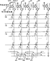
At first, as shown in Figure 1, form multiple bit lines 21 and many word lines 19,26 and dispose mutually orthogonally, TMR element 20 is configured in these line neutrality lines 21 and the memory cell array structure that writes on word line 19 intersection points respectively.The outside in this memory cell array zone is configured in an end that writes word line 19 with current driving circuit 33, and transistor (for example MOSFET) 23 is configured in the other end.
Secondly, we illustrate a-quadrant shown in Figure 1.The ordinary construction of MRAM is represented in this a-quadrant.Promptly, as shown in Figure 2, for example in P type semiconductor substrate (or trap) 11, selectively form the element separated region 12 of STI structure, on Semiconductor substrate 11, selectively form MOSFET13, below two ends of this MOSFET13, for example form the regions and source 14 of N type.Here, MOSFET13 is the switch element that is used to read, and the grid of this MOSFET13 becomes sense word line 26.Again, the 1st contact 16a that will be connected with regions and source 14 on Semiconductor substrate 11 is arranged in the dielectric film 15, on this 1st contact 16a the 1st distribution 17a is set.Equally, in dielectric film 15, the 2nd to the 4th contact 16b is set, 16c, 16d and the 2nd to the 4th distribution 17b, 17c, 17d.Here, the part of the 1st distribution 17a becomes Gnd (ground connection) line 18.Again, the part of the 3rd distribution 17c becomes and writes word line 19a, 19b, 19c.And TMR element 20 is connected with the 4th distribution 17d, and bit line 21 is connected with this TMR element 20.
Secondly, we illustrate B zone shown in Figure 1.The characteristic area of this B region representation in the present invention's the 1st example.That is, as shown in Figure 3, the 3rd contact 16c, the 2nd distribution 17b, the 2nd contact 16b, the 1st distribution 17a, the 1st contact 16a in turn with write word line 19a, 19b, 19c connects.And, the 1st contact 16a and the transistor 23a that on Semiconductor substrate 11, forms, the regions and source 24 of 23b connects.That is, what be formed on adjacency writes word line 19a, imports transistor 23a between the 19b, adjacency write word line 19b, import the structure of transistor 23b between the 19c.
Secondly, we illustrate the structure of TMR element 20.This TMR element 20, as shown in Figure 2, by magnetization adhesive layer (magnetosphere) 41, tunnel junction layer (nonmagnetic layer) 42 and magnetic recording layer (magnetosphere) 43 constitute.And TMR element 20 forms 1 heavy tunnel junction structure as follows or 2 heavy tunnel junction structures, and the whichever structure can.
Fig. 4 A, Fig. 4 B are the sectional views of the TMR element of expression 1 heavy tunnel junction structure.Below, we illustrate the structure of the TMR element of 1 heavy tunnel junction structure.
Equally, TMR element 20 shown in Fig. 4 B is by with template layer 101, initial stage ferromagnetic layer whose 102, antiferromagnetism layer 103, ferromagnetic layer whose 104 ', nonmagnetic layer 107, ferromagnetic layer whose 104 " the lamination magnetization adhesive layer 41 that gets up to form sequentially, the tunnel junction layer 42 that on this magnetization adhesive layer 41, forms; and on this tunnel junction layer 42 sequentially lamination ferromagnetic layer whose 105 '; nonmagnetic layer 107, ferromagnetic layer whose 105 ", the magnetic recording layer 43 that contact layer 106 forms constitutes.
In addition, in the TMR element 20 shown in this Fig. 4 B, by import by the ferromagnetic layer whose 104 in the magnetization adhesive layer 41 ', nonmagnetic layer 107, ferromagnetic layer whose 104 " 3 layers of structure forming; and by the ferromagnetic layer whose 105 in the magnetic recording layer 43 '; nonmagnetic layer 107, ferromagnetic layer whose 105 " 3 layers of structure forming, with the TMR element 20 shown in Fig. 4 A relatively, can provide to be suppressed at the inner magnetic pole that takes place of ferromagnetism, be more suitable for unit structure in miniaturization.
Fig. 5 A, Fig. 5 B are the sectional views that expression has the TMR element of 2 heavy tunnel junction layers.Below, our explanation has the structure of the TMR element 20 of 2 heavy tunnel junction layers.
In addition, in the TMR element 20 shown in this Fig. 5 B, by import by the ferromagnetic layer whose 43 that constitutes magnetic recording layer 43 ', nonmagnetic layer 107, ferromagnetic layer whose 43 " 3 layers of structure forming; and by the ferromagnetic layer whose 104 in the 2nd magnetization adhesive layer 54 '; nonmagnetic layer 107, ferromagnetic layer whose 104 " 3 layers of structure forming, with the TMR element 20 shown in Fig. 5 A relatively, can provide to be suppressed at the inner magnetic pole that takes place of ferromagnetism, be more suitable for unit structure in miniaturization.
The TMR element 20 that has this 2 heavy tunnel junction layers by use, compare with the situation of the TMR element 20 of constructing with 1 heavy tunnel junction, MR (MagnetoResistive when adding identical external bias, magnetic resistance) deterioration than (resistance change rate of one state and " 0 " state) reduces, and can move under higher bias voltage.That is, this is to being favourable when the information in the unit is read into the outside.
The TMR element 20 of this 1 heavy tunnel junction structure or 2 heavy tunnel junction structures can form with following material.
For example, can use Fe, Co, Ni or their alloy, the magnetite that spin polarizability is big, CrO
2, RXMnO
3-y, (R: terres rares, X:Ca, Ba, the Sr) oxide of Denging etc., NiMnSb, PtMnSb etc. all this reins in the material as magnetization adhesive layer 41,51,54 and magnetic recording layer 43 such as alloy.Again, also can be in these magnetics, in not losing ferromagnetic restriction, what comprise some Ag, Cu, Au, Al, Mg, Si, Bi, Ta, B, C, O, N, Pd, Pt, Zr, Ir, W, Mo, the nonmagnetic elements of Nb etc.
Can use Fe-Mn, Pt-Mn, Pt-Cr-Mn, Ni-Mn, Ir-Mn, NiO, Fe
2O
3Deng material as the antiferromagnetism layer 103 that constitutes a part of magnetizing adhesive layer 41.
Can use Al
2O
3, SiO
2, MgO, AlN, Bi
2O
3, MgF
2, CaF
2, SrTiO
2, AlLaO
3Deng various dielectrics as tunnel junction layer 42,52,53 material.In these dielectrics, even if there is oxygen, nitrogen, also it doesn't matter for fluorine damaged.
Below, the information write activity of our explanations in the semiconductor storage relevant with the present invention's the 1st example.
Fig. 6 represents to write distance X between word line and the relation between the current field.In addition, in Fig. 6, the sectional area that writes distribution (write word line 19, write bit line 21) is 0.1J μ m * 0.1 μ m.
As shown in Figure 6, along with the distance X and the variation that writes the current density that flows in the distribution that write between word line, the current field of generation changes.That is, along with the distance X that writes between word line shortens, it is big that the current field of generation becomes, and again along with current density increases, it is big that the current field of generation becomes.
Fig. 7 represents the star-like curve of TMR element.The transverse axis of this star-like curve is represented fixing axial magnetic field, and the longitudinal axis is represented easy axis magnetic field.
Below, we illustrate and use this star-like curve, write " 1 ", " O " information.In addition, in the following description, the distance X that writes between word line is 0.1 μ m.Again, fixing axial distribution is for writing word line 19, and the distribution of easy axis is a bit line 21.
At first, for example when writing " 1 " information, need have the resultant magnetic field in the P zone.That is, need produce the magnetic field of 10Oe for example and produce for example magnetic field about 20~25Oe writing word line 19 at bit line 21.So, in writing word line 19, preferably flow through 5MA/cm
2The electric current of current density preferably flows through 10MA/cm in bit line 21
2The electric current of current density (please refer to Fig. 6).Like this,, the direction of magnetization is changed, can write " 1 " information owing to the resultant magnetic field that has produced in the P zone.
On the other hand, for example when writing " 0 " information, need have the resultant magnetic field in the Q zone.That is, need produce the magnetic field of 10Oe for example and produce for example magnetic field about 20~30Oe writing word line 19 at bit line 21.So, in writing word line 19, preferably flow through 5MA/cm
2The electric current of current density preferably flows through 10MA/cm in bit line 21
2The electric current of current density (please refer to Fig. 6).Like this,, the direction of magnetization is changed, can write " 0 " information owing to the resultant magnetic field that has produced in the Q zone.
Below, our explanation is by in the action that writes between the word line when importing the transistor writing information.
At first, as shown in Figure 1, when information is write the TMR element 20 of any unit 30, select bit line 21b and write word line 19b, at this bit lines 21b with write flowing among the word line 19b P zone that produces Fig. 7 or the electric current 25 of the resultant magnetic field in the Q zone.Here, write word line 19b for electric current 25 is flow through, the transistor 31 of current driving circuit 33 is connected, and also made and this transistor 31 idiostatic transistor 23a, 23b connects.As a result, the electric current 25 that flowing in writing word line 19b is by transistor 23a, and 23b is writing word line 19a, the electric current 25a opposite with electric current 25 directions that flowing respectively among the 19c, 25b.
So, the magnetic field 32 that produces by the electric current 25 that in writing word line 19b, flows and by writing word line 19a, the electric current 25a that flows among the 19c, the magnetic field 32a that 25b produces, 32b becomes opposite peripheral magnetic field.Therefore, the magnetic field 32 that in writing word line 19b, produces, even if arrive 2 adjacent word line 19a that write, 19c, this magnetic field 32 is also by the adjacent word line 19a that writes, the magnetic field 32a that produces among the 19c, 32b offsets.
In addition, as mentioned above, can enough general methods read the information that writes TMR element 20.That is, as shown in Figure 2, by connecting the grid of the MOSFET13 that is connected with the TMR element 20 of writing information, can form from bit line 21 to TMR elements 20, contact 16a, 16b, 16c, 16d, distribution 17a, 17b, 17c, 17d and regions and source 14, the path that electric current flows, the resistance value that can read the TMR element 20 of writing information.Then, can differentiate " 1 ", " 0 " information according to the resistance value of this TMR element 20.
If according to above-mentioned the 1st example, then by importing transistor 23 writing between the word line of adjacency, when writing data, with write word line 19b adjacency write word line 19a, can flow through reciprocal electric current among the 19c.So the magnetic field 32 that is produced by write current 25 is write word line 19a by adjacency, the opposite direction electric current 25a of 19c, the magnetic field 32a that 25b produces, 32b offsets.As a result, because the mistake that can suppress to produce to adjacent unit writes, so can avoid cross-interference issue.
In addition, as shown in Figure 8, also can between the bit line 21 of adjacency, import transistor 23.Further, also can be by with Fig. 1, tectonic association shown in Figure 8 gets up, and the writing between the word line 19 of adjacency, imports transistor 23 between the bit line 21 of adjacency respectively.Also can access the effect in above-mentioned the 1st example in these cases.
(the 2nd example)
The 2nd example is by importing transistor between the word line writing of adjacency, when writing data, with write writing of word line adjacency and flow through reciprocal electric current in the word line.
Fig. 9 is the circuit diagram of the expression semiconductor storage relevant with the present invention's the 2nd example.
Figure 10 is the sectional view that is illustrated in the semiconductor storage in the C zone shown in Figure 9.In addition, because the sectional view of the semiconductor storage in the a-quadrant shown in Figure 9 is identical with Fig. 2 of the 1st example, so omission is to its explanation.
At first, as shown in Figure 9, form multiple bit lines 21 and many word lines 19,26 and dispose mutually orthogonally, TMR element 20 is configured in these line neutrality lines 21 and the memory cell array structure that writes on word line 19 intersection points respectively.The outside in this memory cell array zone is configured in an end that writes word line 19 with current driving circuit 33, and diode 61 is configured in the other end.
Secondly, we illustrate C zone shown in Figure 9.The characteristic area of this C region representation in the present invention's the 2nd example.That is, as shown in figure 10, the 3rd contact 16c, the 2nd distribution 17b, the 2nd contact 16b, the 1st distribution 17a, the 1st contact 16a in turn with write word line 19a, 19b connects.And the 1st contact 16a is connected with the PN junction diode 61 that forms in Semiconductor substrate 11.That is, what be formed on adjacency writes word line 19a, imports the structure of diode 61 between the 19b.
Below, the write activity of our explanations when writing between the word line importing diode.
At first, as shown in Figure 9, when information being write the TMR element 20 of any unit 30, select bit line 21b and write word line 19b, at this bit lines 21b with write flowing among the word line 19b P zone that produces Fig. 7 or the electric current 25 of the resultant magnetic field in the Q zone.Here,, on the transistor 31 of current driving circuit 33, add bias voltage, make electric current 25 also flow through diode 61a, 61b along direction in order in writing word line 19b, to flow through electric current 25.As a result, writing word line 19a, the electric current 25a opposite that flowing respectively among the 19c, 25b with electric current 25 directions.
So, the magnetic field 32 that produces by the electric current 25 that in writing word line 19b, flows and by writing word line 19a, the electric current 25a that flows among the 19c, the magnetic field 32a that 25b produces, 32b becomes opposite peripheral magnetic field.Therefore, write the magnetic field 32 that word line 19b produces, even if arrive 2 adjacent word line 19a that write, 19c, this magnetic field 32 is also by the adjacent word line 19a that writes, the magnetic field 32a that 19c produces, 32b offsets.
In addition, as mentioned above, because use the method identical to read the information that writes TMR element 20, so omit to reading the explanation of action with the 1st example.
If according to the 2nd example, then can access the effect identical with the 1st example.
In addition, as shown in figure 11, also can between the bit line 21 of adjacency, import diode 61.Further, also can be by with Fig. 9, tectonic association shown in Figure 11 gets up, and the writing between the word line 19 of adjacency, imports diode end 61 between the bit line 21 of adjacency respectively.Also can access the effect in above-mentioned the 2nd example in these cases.
(the 3rd example)
The 3rd example is the variation of the 1st example, replaces transistor as the switch element that is used to read with diode.
Figure 12 is the circuit diagram of the expression semiconductor storage relevant with the present invention's the 3rd example.Figure 13 is the sectional view that is illustrated in the semiconductor storage in the D zone shown in Figure 12.
As shown in figure 12, the B zone, identical with the 1st example, what be formed on adjacency writes word line 19a, imports transistor 23a between the 19b, adjacency write word line 19b, import the structure of transistor 23b between the 19c.
As shown in figure 13, the D zone, formation is configured in TMR element 20 bit line 21 and writes word line 19a, 19b, on each intersection point of 19c, the structure that PN junction diode 71 and this TMR element 20 are connected in series.
Because it is identical with above-mentioned the 1st example that this information in the 3rd example writes, so omission is to its explanation.On the other hand, following information of carrying out in the 3rd example is read.That is, flow through the diode 71 that is connected with the TMR element 20 of writing information, adjust bias voltage, the resistance value of reading the TMR element 20 that is connected with this diode 71 in order to make electric current.Then, can differentiate " 1 " " 0 " information according to the resistance value of this TMR element 20.
If according to above-mentioned the 3rd example, then can access the effect identical with the 1st example.
Further,, compare, can dwindle the special-purpose area in memory cell array zone with the 1st and the 2nd example by using diode 71 as switch element.
In addition, as shown in figure 14, also can between the bit line 21 of adjacency, import transistor 23.Further, also can be by with Figure 12, tectonic association shown in Figure 14 gets up, and the writing between the word line 19 of adjacency, imports transistor 23 between the bit line 21 of adjacency respectively.Also can access the effect in above-mentioned the 3rd example in these cases.
(the 4th example)
The 4th example is the variation of the 2nd example, replaces transistor as the switch element that is used to read with diode.
Figure 15 is the circuit diagram of the expression semiconductor storage relevant with the present invention's the 4th example.As shown in figure 15, the C zone, identical with the 2nd example, what be formed on adjacency writes word line 19a, imports diode 61a between the 19b, adjacency write word line 19b, import the structure of diode 61b between the 19c.On the other hand, the D zone, identical with the 3rd example, formation is configured in bit line 21 with TMR element 20 and writes on the intersection point of word line 19, the structure that PN junction diode 71 and this TMR element 20 are connected in series.
Because it is identical with above-mentioned the 2nd example that this information in the 4th example writes, so omission is to its explanation.On the other hand, identical because the information in the 4th example is read with above-mentioned the 3rd example, so omission is to its explanation.
If according to above-mentioned the 4th example, then can access the effect identical with the 2nd example.
Further,, compare, can dwindle the special-purpose area in memory cell array zone with the 1st and the 2nd example by using diode 71 as switch element.
In addition, as shown in figure 16, also can between the bit line 21 of adjacency, import diode 61.Further, also can be by with Figure 15, tectonic association shown in Figure 16 gets up, and the writing between the word line 19 of adjacency, imports diode 61 between the bit line 21 of adjacency respectively.Also can access the effect in above-mentioned the 4th example in these cases.
In each example as described above, also can use by 2 magnetospheres and GMR (Giant Magneto Resistive, the giant magnetoresistance) element formed by the conductor layer of these magnetosphere clampings to replace the TMR element.In above-mentioned each example, can suitably change the structure in memory cell array zone again.
For those skilled in the art, can easily understand all additional advantages and modification.So the present invention is not limited to detail and the representational example of representing and describing at it here aspect widely.Therefore, we can carry out various modification and not depart from spirit and scope by the general inventive concept of appended claims and equivalent thereof definition.
Claims (15)
1. semiconductor storage, it possesses:
At the upwardly extending multiple bit lines of the 1st side,
The a plurality of magnetic elements that are connected with above-mentioned bit line,
Clip above-mentioned magnetic element from the two opposite sides of above-mentioned magnetic element together at the upwardly extending and above-mentioned bit line of the 2nd side different with above-mentioned the 1st direction, and many word lines that dispose separatedly with above-mentioned magnetic element and
The 1st transistor or the 1st diode that is connected with the above-mentioned word line of adjacency respectively, above-mentioned the 1st transistor or above-mentioned the 1st diode arrangement are in the outside in the memory cell array zone that has disposed above-mentioned magnetic element.
2. semiconductor storage, it possesses:
At the upwardly extending multiple bit lines of the 1st side,
The a plurality of magnetic elements that are connected with above-mentioned bit line,
Clip above-mentioned magnetic element from the two opposite sides of above-mentioned magnetic element together at the upwardly extending and above-mentioned bit line of the 2nd side different with above-mentioned the 1st direction, and many word lines that dispose separatedly with above-mentioned magnetic element and
The 2nd transistor or the 2nd diode that is connected with the above-mentioned bit line of adjacency respectively, above-mentioned the 2nd transistor or above-mentioned the 2nd diode arrangement are in the outside in the memory cell array zone that has disposed above-mentioned magnetic element.
3. according to the semiconductor storage of claim 1, it further possesses
The 2nd transistor or the 2nd diode that is connected with the above-mentioned bit line of adjacency respectively.
4. according to the semiconductor storage of claim 1, it further possesses
The 3rd transistor that is connected with above-mentioned magnetic element or the 3rd diode.
5. according to the semiconductor storage of claim 2, it further possesses
The 3rd transistor that is connected with above-mentioned magnetic element or the 3rd diode.
6. according to the semiconductor storage of claim 1,
Above-mentioned magnetic element is by the 1st magnetosphere, the TMR element of at least 3 layers of formation of the 2nd magnetosphere and nonmagnetic layer.
7. according to the semiconductor storage of claim 2,
Above-mentioned magnetic element is by the 1st magnetosphere, the TMR element of at least 3 layers of formation of the 2nd magnetosphere and nonmagnetic layer.
8. according to the semiconductor storage of claim 6,
Above-mentioned TMR element is that 1 weight structure with above-mentioned nonmagnetic layer of 1 layer is made or 2 weight structures with above-mentioned nonmagnetic layer of 2 layers are made.
9. according to the semiconductor storage of claim 7,
Above-mentioned TMR element is that 1 weight structure with above-mentioned nonmagnetic layer of 1 layer is made or 2 weight structures with above-mentioned nonmagnetic layer of 2 layers are made.
10. according to the semiconductor storage of claim 1,
Above-mentioned magnetic element is by the 1st magnetosphere, the GMR element of at least 3 layers of formation of the 2nd magnetosphere and conductor layer.
11. according to the semiconductor storage of claim 2,
Above-mentioned magnetic element is by the 1st magnetosphere, the GMR element of at least 3 layers of formation of the 2nd magnetosphere and conductor layer.
12. according to the semiconductor storage of claim 1,
Above-mentioned the 1st direction and above-mentioned the 2nd direction quadrature.
13. according to the semiconductor storage of claim 2,
Above-mentioned the 1st direction and above-mentioned the 2nd direction quadrature.
14. according to the semiconductor storage of claim 1,
When information being write arbitrarily above-mentioned magnetic element, by in the word line of selecting on the 3rd direction streaming current, make this electric current flow through above-mentioned the 1st transistor or above-mentioned the 1st diode, above-mentioned electric current with the word line of the above-mentioned word line adjacency of selecting on 4th direction opposite, flow with above-mentioned the 3rd direction.
15. according to the semiconductor storage of claim 2,
When information being write arbitrarily above-mentioned magnetic element, by in the bit line of selecting on the 5th direction streaming current, make this electric current flow through above-mentioned the 2nd transistor or above-mentioned the 2nd diode, above-mentioned electric current with the bit line of the above-mentioned bit line adjacency of selecting on 6th direction opposite, flow with above-mentioned the 5th direction.
Applications Claiming Priority (4)
| Application Number | Priority Date | Filing Date | Title |
|---|---|---|---|
| JP399223/2000 | 2000-12-27 | ||
| JP2000399223 | 2000-12-27 | ||
| JP2001373071A JP2002270790A (en) | 2000-12-27 | 2001-12-06 | Semiconductor storage device |
| JP373071/2001 | 2001-12-06 |
Publications (2)
| Publication Number | Publication Date |
|---|---|
| CN1363955A CN1363955A (en) | 2002-08-14 |
| CN1244154C true CN1244154C (en) | 2006-03-01 |
Family
ID=26606944
Family Applications (1)
| Application Number | Title | Priority Date | Filing Date |
|---|---|---|---|
| CNB011439599A Expired - Fee Related CN1244154C (en) | 2000-12-27 | 2001-12-27 | Semiconductor storaging device |
Country Status (5)
| Country | Link |
|---|---|
| US (1) | US6661689B2 (en) |
| JP (1) | JP2002270790A (en) |
| KR (1) | KR100431483B1 (en) |
| CN (1) | CN1244154C (en) |
| TW (1) | TW521426B (en) |
Families Citing this family (22)
| Publication number | Priority date | Publication date | Assignee | Title |
|---|---|---|---|---|
| JP4656720B2 (en) * | 2000-09-25 | 2011-03-23 | ルネサスエレクトロニクス株式会社 | Thin film magnetic memory device |
| JP3808799B2 (en) | 2002-05-15 | 2006-08-16 | 株式会社東芝 | Magnetic random access memory |
| US7042749B2 (en) * | 2002-05-16 | 2006-05-09 | Micron Technology, Inc. | Stacked 1T-nmemory cell structure |
| WO2003098636A2 (en) * | 2002-05-16 | 2003-11-27 | Micron Technology, Inc. | STACKED 1T-nMEMORY CELL STRUCTURE |
| US6940748B2 (en) * | 2002-05-16 | 2005-09-06 | Micron Technology, Inc. | Stacked 1T-nMTJ MRAM structure |
| US6801450B2 (en) * | 2002-05-22 | 2004-10-05 | Hewlett-Packard Development Company, L.P. | Memory cell isolation |
| JP4322481B2 (en) * | 2002-08-12 | 2009-09-02 | 株式会社東芝 | Semiconductor integrated circuit device |
| JP3906139B2 (en) * | 2002-10-16 | 2007-04-18 | 株式会社東芝 | Magnetic random access memory |
| JP4290494B2 (en) * | 2003-07-08 | 2009-07-08 | 株式会社ルネサステクノロジ | Semiconductor memory device |
| US7166881B2 (en) * | 2003-10-13 | 2007-01-23 | Taiwan Semiconductor Manufacturing Company, Ltd. | Multi-sensing level MRAM structures |
| KR100527536B1 (en) * | 2003-12-24 | 2005-11-09 | 주식회사 하이닉스반도체 | Magnetic random access memory |
| US7884403B2 (en) | 2004-03-12 | 2011-02-08 | Japan Science And Technology Agency | Magnetic tunnel junction device and memory device including the same |
| US6946698B1 (en) | 2004-04-02 | 2005-09-20 | Taiwan Semiconductor Manufacturing Company, Ltd. | MRAM device having low-k inter-metal dielectric |
| US7099176B2 (en) * | 2004-04-19 | 2006-08-29 | Taiwan Semiconductor Manufacturing Company, Ltd. | Non-orthogonal write line structure in MRAM |
| US7265053B2 (en) * | 2004-04-26 | 2007-09-04 | Taiwan Semiconductor Manufacturing Company, Ltd. | Trench photolithography rework for removal of photoresist residue |
| US20060039183A1 (en) * | 2004-05-21 | 2006-02-23 | Taiwan Semiconductor Manufacturing Co., Ltd. | Multi-sensing level MRAM structures |
| US7221584B2 (en) * | 2004-08-13 | 2007-05-22 | Taiwan Semiconductor Manufacturing Company, Ltd. | MRAM cell having shared configuration |
| US7170775B2 (en) * | 2005-01-06 | 2007-01-30 | Taiwan Semiconductor Manufacturing Company, Ltd. | MRAM cell with reduced write current |
| JP2007317824A (en) | 2006-05-25 | 2007-12-06 | Tdk Corp | Magnetoresistance effect element, its manufacturing method, thin film magnetic head, head jimbal assembly, head arm assembly, and magnetic disk drive |
| JP4384137B2 (en) | 2006-06-14 | 2009-12-16 | Tdk株式会社 | Method of manufacturing magnetic field detection element for CPP-GMR head, magnetic field detection element for CPP-GMR head, laminate, wafer, head gimbal assembly, and hard disk device |
| JP5412640B2 (en) | 2008-11-13 | 2014-02-12 | ルネサスエレクトロニクス株式会社 | Magnetic memory device |
| CN105449099B (en) * | 2015-10-15 | 2018-04-06 | 上海磁宇信息科技有限公司 | Cross matrix column magnetic RAM and its reading/writing method |
Family Cites Families (14)
| Publication number | Priority date | Publication date | Assignee | Title |
|---|---|---|---|---|
| JP3392657B2 (en) * | 1996-09-26 | 2003-03-31 | 株式会社東芝 | Semiconductor storage device |
| JP4124844B2 (en) | 1997-10-02 | 2008-07-23 | キヤノン株式会社 | Magnetic thin film memory |
| JP3593472B2 (en) * | 1998-06-30 | 2004-11-24 | 株式会社東芝 | Magnetic element, magnetic memory and magnetic sensor using the same |
| JP2000132961A (en) * | 1998-10-23 | 2000-05-12 | Canon Inc | Magnetic thin film memory, method for reading out magnetic thin film memory, and method for writing to magnetic thin film memory |
| JP3803503B2 (en) | 1999-04-30 | 2006-08-02 | 日本電気株式会社 | Magnetic random access memory circuit |
| JP2001217398A (en) | 2000-02-03 | 2001-08-10 | Rohm Co Ltd | Storage device using ferromagnetic tunnel junction element |
| DE10020128A1 (en) | 2000-04-14 | 2001-10-18 | Infineon Technologies Ag | MRAM memory |
| JP4477199B2 (en) | 2000-06-16 | 2010-06-09 | 株式会社ルネサステクノロジ | Magnetic random access memory, method for accessing magnetic random access memory, and method for manufacturing magnetic random access memory |
| JP2002170377A (en) * | 2000-09-22 | 2002-06-14 | Mitsubishi Electric Corp | Thin film magnetic storage device |
| JP4726290B2 (en) * | 2000-10-17 | 2011-07-20 | ルネサスエレクトロニクス株式会社 | Semiconductor integrated circuit |
| DE10053965A1 (en) * | 2000-10-31 | 2002-06-20 | Infineon Technologies Ag | Method for preventing unwanted programming in an MRAM arrangement |
| JP2002216468A (en) * | 2000-11-08 | 2002-08-02 | Canon Inc | Semiconductor memory device |
| JP4637388B2 (en) * | 2001-03-23 | 2011-02-23 | ルネサスエレクトロニクス株式会社 | Thin film magnetic memory device |
| JP2003016777A (en) * | 2001-06-28 | 2003-01-17 | Mitsubishi Electric Corp | Thin film magnetic storage device |
-
2001
- 2001-12-06 JP JP2001373071A patent/JP2002270790A/en active Pending
- 2001-12-14 TW TW090131068A patent/TW521426B/en not_active IP Right Cessation
- 2001-12-26 KR KR10-2001-0085014A patent/KR100431483B1/en not_active IP Right Cessation
- 2001-12-26 US US10/025,753 patent/US6661689B2/en not_active Expired - Fee Related
- 2001-12-27 CN CNB011439599A patent/CN1244154C/en not_active Expired - Fee Related
Also Published As
| Publication number | Publication date |
|---|---|
| JP2002270790A (en) | 2002-09-20 |
| CN1363955A (en) | 2002-08-14 |
| TW521426B (en) | 2003-02-21 |
| US6661689B2 (en) | 2003-12-09 |
| KR100431483B1 (en) | 2004-05-14 |
| US20020080641A1 (en) | 2002-06-27 |
| KR20020053752A (en) | 2002-07-05 |
Similar Documents
| Publication | Publication Date | Title |
|---|---|---|
| CN1244154C (en) | Semiconductor storaging device | |
| CN1280829C (en) | Magnetic storage device | |
| CN1206656C (en) | Magnetic random access memory | |
| CN1283006C (en) | Magnetic storage device and mfg. method | |
| KR101869149B1 (en) | Voltage-controlled magnetic anisotropy switching device using an external ferromagnetic biasing film | |
| KR100518284B1 (en) | Semiconductor memory device | |
| CN1215464C (en) | Magnetic recorder and mfg. method thereof | |
| CN1345091A (en) | Semiconductor storage using tunnel magneto-resistance effect and manufacture thereof | |
| CN1745429A (en) | MRAM architecture for low power consumption and high selectivity | |
| CN100350495C (en) | Magneto-resistive device having magnetically soft reference | |
| CN1851823A (en) | Magnetic random access memory device | |
| CN1713299A (en) | Magnetic memory unit and fabricating method thereof | |
| KR101476491B1 (en) | Spin valve element and its driving method and storage device employing them | |
| CN1414559A (en) | Storage device which-storage cell having series magnetic tunnel junction and tunnel junction | |
| CN1612262A (en) | System and method for storing data in an unpatterned, continuous magnetic layer | |
| CN1747060A (en) | The method of operating magnetic random access memory device using spin injection and related device | |
| CN100350496C (en) | Magnetic storage device and its manufacturing method | |
| JP2009152258A (en) | Unidirectional current magnetism inversion magnetoresistive element and magnetic recording device | |
| CN1187824C (en) | Semiconductor device and its mfg. method | |
| CN101625890B (en) | Operation method of magnetic random access memory device | |
| US20140119106A1 (en) | Magnetic memory devices and methods of operating the same | |
| CN100481252C (en) | Buried magnetic tunnel junction storage cell and method | |
| CN101047227A (en) | Nano magnetic memory device and method of manufacturing the same | |
| CN1499521A (en) | Magnetic memory element using metal inlaid tech and its mfg. method | |
| WO2019092816A1 (en) | Tunnel magnetoresistive effect element, magnetic memory, and built-in memory |
Legal Events
| Date | Code | Title | Description |
|---|---|---|---|
| C10 | Entry into substantive examination | ||
| SE01 | Entry into force of request for substantive examination | ||
| C06 | Publication | ||
| PB01 | Publication | ||
| C14 | Grant of patent or utility model | ||
| GR01 | Patent grant | ||
| C17 | Cessation of patent right | ||
| CF01 | Termination of patent right due to non-payment of annual fee |
Granted publication date: 20060301 Termination date: 20121227 |