CN1224876C - Clock synchronous circuit - Google Patents
Clock synchronous circuit Download PDFInfo
- Publication number
- CN1224876C CN1224876C CNB021303754A CN02130375A CN1224876C CN 1224876 C CN1224876 C CN 1224876C CN B021303754 A CNB021303754 A CN B021303754A CN 02130375 A CN02130375 A CN 02130375A CN 1224876 C CN1224876 C CN 1224876C
- Authority
- CN
- China
- Prior art keywords
- state
- holding unit
- clock
- impulse
- state holding
- Prior art date
- Legal status (The legal status is an assumption and is not a legal conclusion. Google has not performed a legal analysis and makes no representation as to the accuracy of the status listed.)
- Expired - Fee Related
Links
Images


Classifications
-
- G—PHYSICS
- G11—INFORMATION STORAGE
- G11C—STATIC STORES
- G11C7/00—Arrangements for writing information into, or reading information out from, a digital store
- G11C7/22—Read-write [R-W] timing or clocking circuits; Read-write [R-W] control signal generators or management
- G11C7/222—Clock generating, synchronizing or distributing circuits within memory device
-
- G—PHYSICS
- G11—INFORMATION STORAGE
- G11C—STATIC STORES
- G11C7/00—Arrangements for writing information into, or reading information out from, a digital store
- G11C7/22—Read-write [R-W] timing or clocking circuits; Read-write [R-W] control signal generators or management
-
- H—ELECTRICITY
- H03—ELECTRONIC CIRCUITRY
- H03K—PULSE TECHNIQUE
- H03K5/00—Manipulating of pulses not covered by one of the other main groups of this subclass
- H03K5/13—Arrangements having a single output and transforming input signals into pulses delivered at desired time intervals
- H03K5/135—Arrangements having a single output and transforming input signals into pulses delivered at desired time intervals by the use of time reference signals, e.g. clock signals
Abstract
For a reset operation of a state-holding section after monitoring a delay time necessary for synchronizing an external clock with an internal clock, a state-holding unit of an n-th stage is reset, when a state-holding unit of a subsequent stage is in a reset state (Qn+1''L'') in a reset period (bP2=''L''). A reset stage number is determined by a length of the reset period, and is always constant. The fact that an output signal bRCLn-2 of the pre-previous stage degenerative delay unit is put into an 'L' state may be added to a reset condition.
Description
The cross reference of related application
The application based on and advocate the right of priority of the 2001-202552 of Japanese patent application formerly that submits to July 3 calendar year 2001, here by with reference to introducing its full content.
Technical field
The present invention relates to a kind of use high-frequency clocks such as Double Data Rate (DDR) type DRAM, synchronous dram (SDRAM) and Double Data Rate period 1 (double data rate first cycle) RAM (FCRAM) isochronon synchronized model storer that are applicable to and carry out the clock synchronization circuit of synchro control.
Background technology
In recent years, in computer system, should handle the requirement of high speed, adopt synchronous dram isochronon synchronized model storer.This clock synchronization type storer is at clock (hereinafter referred to as external clock) the synchronous clock of memory inside use with control store.
But, because the influence of receiver (input buffer) etc., between clock (hereinafter referred to as internal clocking) that memory inside is used and external clock, produce under the situation of deviation (time lag), particularly for high speed motion, even this deviation is very little, also in the internal circuit of storer, cause maloperation easily.In addition, use with external clock internal clocking devious to come also can hinder high speed processing owing to the controller of these data of use from the data of storer output.
Therefore, in nearest storer, make synchronous with the external clock accurately clock synchronization circuit of internal clocking in chip internal set.
In the past, for the structure of clock synchronization circuit, known periods type and two kinds on bit comparison type mutually.Particularly, compare with the clock synchronization circuit of bit comparison type mutually, (from power connection to finishing the synchronous speed of external clock and internal clocking) soon because synchronous speed as the STBD (Synchronous Traced Backward Delay) of preiodic type clock synchronization circuit, so frequent relay is to realize consuming the minimizing of function.
Fig. 1 is the block structure of the existing preiodic type clock synchronization circuit of expression.
Input external clock EXTCLK in the receiver with retardation Trc (input buffer) 11.Receiver 11 outputs have the clock CLKSTIN of Trc time lag to external clock EXTCLK.Clock CLKSTIN input had delay monitor 12 and the control pulse generation circuit 13 that retardation is Trc+Tdr.
Postpone monitor 12 according to clock CLKSTIN output direct impulse FCLIN.Control pulse generation circuit 13 is according to clock CLKSTIN output control pulse P, bP.Control pulse generation circuit 13 is made of circuit for example shown in Figure 6.
Direct impulse FCLIN is imposed on direct impulse lag line 14.Direct impulse with lag line 14 by the N that is connected in series forward delay cell 14-1, a 14-2 ... 14-n ... 14-N constitutes.Wherein, N and n are positive number, and n<N.
Gating pulse (direct impulse transmission of control signals) P, bP control N forward delay cell 14-1,14-2 ... 14-n ... the action of 14-N.When N forward delay cell 14-1,14-2 ... 14-n ... when 14-N was in operating state (can transmit the state of direct impulse), the direct impulse that each forward delay cell will receive from the forward delay cell of prime was transferred to the forward delay cell of back level.
Forward delay cell 14-n is made of for example circuit shown in Figure 2.
The forward delay cell of input direct impulse changes the state (set/reset) of the state holding unit corresponding with it.Particularly, before direct impulse FCLIN input direct impulse is used lag line 14, all state holding unit 15-1,15-2 ... 15-n ... 15-N is in (R) state that resets, and becomes set (S) state corresponding to the state holding unit of forward delay cell of input direct impulse from (R) state that resets.
State holding unit 15-n is made of for example circuit shown in Figure 3.
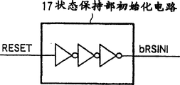
N state holding unit 15-1,15-2 in the state retaining part 15 ... 15-n ... 15-N recovers reset mode by gating pulse (state retaining part reset signal) bP.State retaining part initializing circuit 17 is according to reset signal RESET output initializing signal bRSINI, force with N state holding unit 15-1,15-2 ... 15-n ... the state of 15-N is initialized as reset mode.
State retaining part initializing circuit 17 is made of for example circuit shown in Figure 14.
Postpone monitor 12, control pulse generation circuit 13, direct impulse and be to monitor the synchronous required delay time T of external clock EXTCLK and internal clocking INTCLK-(Trc-Tdr) with the purpose of lag line 14, state retaining part 15 and state retaining part initializing circuit 17, here, be called monitoring circuit.
With respect to the monitoring circuit that monitors delay time T-(Trc-Tdr), reverse impulse is correctly to duplicate the delay time T of monitor circuit monitors-(Trc-Tdr) with the purpose of lag line 16.
Because reverse impulse is correct replica delay time τ-(Trc-Tdr) with the purpose of lag line 16, so copy direct impulse fully with lag line 14.That is, be symmetrical in hold mode portion 15 and dispose direct impulse lag line 14 and reverse impulse lag line 16, and two circuit structures are identical.Therefore, the STBD of this example is called as mirror STBD sometimes.
Reverse impulse with lag line 16 by the N that is connected in series revertive delay unit 16-1, a 16-2 ... 16-n ... 16-N constitutes.Reverse impulse with lag line 16 according to N state holding unit 15-1,15-2 in the state retaining part 15 ... 15-n ... the state of 15-N and CLKSTIN, at correct replica delay time τ-(Trc-Tdr) afterwards, export clock STCLK.
Revertive delay unit 16-n is made of for example circuit shown in Figure 5.
Clock STCLK is in case through having the driver 18 of retardation Tdr, then become the internal clocking INTCLK synchronous with external clock EXTCLK.
The following describes the synchronization action principle of STBD.
Wherein, STBD as shown in Figure 1, the forward delay cell 15-n of n level changes the state of the state holding unit 15-n of n level, according to the state of n level state holding unit 15-n, n-1 level revertive delay unit 16-(n-1) action.
Fig. 7 is the oscillogram of the synchronization action principle of explanation STBD.
Consider the situation of the external clock EXTCLK input receiver 11 of period tau shown in the figure (a).
External clock EXTCLK carries out wave shaping and amplification by receiver 11, exports as clock CLKSTIN.If establish when time delay that receiver 11 has being Trc, then clock CLKSTIN has only postponed Trc with respect to external clock EXTCLK.(figure (b)).
Import display monitor (conformable display) 12, control pulse generation circuit 13, reverse impulse lag line 16 respectively from the clock CLKSTIN of receiver 11 outputs.
Control pulse generation circuit 13 chopping CLKSTIN generate the gating pulse P that rises synchronously with clock CLKSTIN.For example, cycle of gating pulse P is set at τ, pulse width is set at Wp (figure (c)).Gating pulse bP is the reverse signal of gating pulse P.
Postpone monitor 12 have equal that receiver 11 has time delay Trc and driver 14 have time delay the Tdr sum time delay (Trc+Tdr).Therefore, only postpone (Trc+Tdr) with respect to clock CLKSTIN from receiver 11 outputs from the direct impulse FCLIN that postpones monitor 12 outputs, and input direct impulse lag line 14 (figure (d)).
Direct impulse with lag line 14 by the N that is connected in series forward delay cell 14-1, a 14-2 ... 14-n ... 14-N constitutes.N forward delay cell 14-1,14-2 ... 14-n ... when each of 14-N at gating pulse P is " L (low) " level, receive from the direct impulse of prime forward delay cell output, level forward delay cell is transmitted this direct impulse backward.In addition, N forward delay cell 14-1,14-2 ... 14-n ... when each of 14-N at gating pulse P is " H (height) " level, stop the direct impulse transmission of direct impulse with lag line 14.
That is, direct impulse FCLIN only from be input to lag line 14 to direct impulse gating pulse P become " H " level during in (τ-(Trc+Tdr)) the transmission direct impulse with lag line 14 (figure (d)).
The transmission state of state retaining part 15 storage direct impulses, in acquired information, the control reverse impulse makes the reverse impulse of reverse impulse identical with the transmission time in the lag line 14 with the direct impulse of direct impulse with the transmission time in the lag line 16 with the action of each the revertive delay unit in the lag line 16.
The revertive delay unit that is in the state holding unit control of SM set mode is configured in the output signal of the revertive delay unit of back level to the revertive delay unit former state output that is configured in its prime.The revertive delay unit of state holding unit control that remains on reset mode is to the output signal of the revertive delay unit output receiver 11 that is configured in its prime.
The state retaining part 15 of original state by state retaining part initializing circuit 17 with all state holding unit 15-1,15-2 ... 15-n ... 15-N becomes reset mode, corresponding to the state holding unit former state hold reset state of the forward delay cell of not importing direct impulse, become SM set mode corresponding to the state holding unit of forward delay cell of input direct impulse.
When gating pulse P becomes " H " level, clock CLKSTIN also becomes H level (figure (b), (c)), so import the input signal (CLKSTIN) of H level to the revertive delay unit (for example later revertive delay unit of the n level of Figure 26) that the state holding unit of reset mode is controlled.
If establishing the progression of the forward delay cell of direct impulse transmission is n, then state holding unit 15-1, the 15-2 of the 1st~n ... 15-n becomes SM set mode, so the n level revertive delay unit 16-n of the state holding unit control of (n+1) of reset mode level generates reverse impulse, reverse impulse is transferred to the revertive delay unit 16-(n-1) of its prime from revertive delay unit 16-n.
Therefore, the revertive delay unit progression of reverse impulse transmission equates with the forward delay cell progression of direct impulse transmission.
Here, the direct impulse of direct impulse was designed to be equal to each other with the reverse impulse of transmission time (time delay) of lag line 14 and the reverse impulse transmission time (time delay) with lag line 16, thus from direct impulse FCLIN input direct impulse with lag line 14 to being (τ-(Trc+Tdr)) * 2 (scheming (e)) with time of lag line 16 output reverse impulse STCLK from reverse impulse.
Afterwards, will be from reverse impulse (clock) the STCLK enter drive 18 of reverse impulse with lag line 16 outputs.Driver 18 has Tdr time delay, so the output signal of driver 18 becomes the internal clocking INTCLK synchronous with external clock EXTCLK (figure (f)).
To begin to have to receiver 11 input external clock EXTCLK to calculating as Δ total from the time delay of driver 18 output internal clocking INTCLK
Δtotal=Δmsr+Δprp (1)。
Wherein, Δ msr is from beginning to blocking in the time of direct impulse with transmission direct impulse in the lag line 14 to postponing monitor 12 input direct impulses, Δ prp be from block direct impulse with lag line 14 in the transmission direct impulse begin to use the total ascent time of the retardation of time of the reverse impulse of generation in the lag line 16 and receiver 11 to export reverse impulses to driver 18.
Postpone monitor 12 and have retardation (Trc+Tdr), direct impulse be (τ-(Trc+Tdr)) at direct impulse with time of transmission in the lag line 14, uses following formula (2) to represent Δ msr:
Δmsr=(Trc+Tdr)+(τ-(Trc+Tdr))=τ (2)
Δprp=Trc+(τ-(Trc+Tdr))+Tdr=τ (3)
By above-mentioned (3) formula, getting Δ prp is τ, the result, and internal clocking INTCLK and external clock EXTCLK are synchronous.
According to above-mentioned (1)-(3) formula, from beginning in the external clock EXTCLK input chip (particularly being receiver 11) to generating, be 2 τ with required time of the synchronous internal clocking INTCLK of external clock EXTCLK.
Thus, in STBD as the preiodic type clock synchronization circuit, from beginning to shorten to 2 τ in the external clock EXTCLK input chip to generating the required time of internal clocking INTCLK, compare with the clock synchronization circuit of bit comparison type mutually, synchronous speed (from power connection to finishing the synchronous speed of external clock and internal clocking) accelerates.Therefore, often existence do not make memory-aided during, even under very short during this period situation, all can carry out power supply at every turn and disconnect, realize the minimizing of consumption power.
In addition, in existing preiodic type clock synchronization circuit, make under the memory-aided situation in connection, external clock EXTCLK only once monitors action in one number time, the state of the state retaining part 15 that this supervision action is obtained was fixed between the one number time of external clock EXTCLK, and can realize the minimizing of consumed power.
But there is following problem in this method.
That is, in fact when action memory, the generation cycle changes among the external clock EXTCLK, and in addition, the environment temperature of chip also changes.At this moment, the direct impulse unit progression instability of direct impulse transmission is corresponding to variations such as the cyclical swing of external clock EXTCLK or chip environment temperatures.
Therefore, when the state with state retaining part 15 is fixed between the one number time of external clock EXTCLK, in this one number time, externally produce synchronism deviation between clock EXTCLK and the internal clocking INTCLK, can not synchronous accurately two clocks.
For example, as shown in Figure 8, consider that for the transmission progression of k direct impulse in the cycle, the direct impulse transmission progression in the k+1 cycle only increases the situation of δ owing to influences such as temperature changes.At this moment, as if each cycle is all carried out the supervision of external clock EXTCLK, usually obtain the internal clocking INTCLK synchronous with external clock EXTCLK, no problem, but when not carrying out external clock EXTCLK supervision, can not obtain the internal clocking INTCLK synchronous with external clock EXTCLK in each cycle.
In addition, as shown in Figure 9, consider that for the transmission progression of k direct impulse in the cycle, the direct impulse transmission progression in the k+1 cycle only reduces the situation of δ owing to influences such as temperature changes.At this moment, as if each cycle is all carried out the supervision of external clock EXTCLK, usually obtain the internal clocking INTCLK synchronous with external clock EXTCLK, no problem, but when not carrying out external clock EXTCLK supervision, can not obtain the internal clocking INTCLK synchronous with external clock EXTCLK in each cycle.
Therefore,, then can improve synchronization accuracy, but consumed power becomes big as if each cycle is monitored action.On the contrary, as if several cycles are monitored action, then consumed power diminishes, but synchronization accuracy reduces.
In recent years, the variation of the transmission progression of the direct impulse that influences such as temperature change cause has the tendency that diminishes, and in fact, considers consumed power and synchronization accuracy, regularly (each cycle or whenever several cycles) monitor action.
Under the situation of Fig. 9, regularly for example each cycle is carried out the supervision of external clock EXTCLK, in the cycle, at least the n level and n+1 level state holding unit must become (R) state that resets at k+1.
That is, because the transmission progression of the direct impulse of the k+1 cycle under only reduces δ with respect to the transmission progression of the direct impulse of the k cycle under, thus corresponding with it, the also necessary minimizing of the quantity of the state holding unit of set (S) state.Therefore, before the k+1 cycle begins, must return reset mode (below this action being called homing action) from SM set mode corresponding to the state holding unit of δ (with dashed lines surrounds among Fig. 9) or the state holding unit (unit before the n-1 level) that comprises it.
In preiodic type clock synchronization circuit (STBD, SMD etc.), state holding unit 15-1, the 15-2 among the STBD in the state retaining part 15 ... 15-n ... 15-N has latch circuit.
As latch circuit, only can adopt at the appointed time during in keep the dynamic type latch circuit of its state gained and be limited to the static type latch circuit that does not carry out resetting etc., keeps its state usually, but under any circumstance, particularly consider the situation of Fig. 9, after monitoring action, be necessary next monitor be equipped with in the action carry out homing action come in the reset mode retaining part 15 state holding unit 15-1,15-2 ... 15-n ... the state of 15-N.
In addition, the homing action that (each cycle or whenever several cycles) carries out in the past about has regularly been considered the whole bag of tricks, but has been failed to propose to realize simultaneously the method for low consumpting power, high synchronization accuracy, simple layout, little circuit size etc.
Therefore, for using latch circuit will monitor that the result keeps the clock synchronization circuit during certain, must be regularly, be that homing action and the clock supervision of carrying out the interior state holding unit of state retaining part in each external clock EXTCLK cycle or every a plurality of cycle moved.But, also fail to propose to realize simultaneously the clock synchronization circuit of low consumpting power, high synchronization accuracy, simple layout, little circuit size etc.
Summary of the invention
In order to overcome above-mentioned the problems of the prior art, the invention provides a kind of clock synchronization circuit, make the synchronous synchronization action of first clock and second clock, comprising: receive the described second clock with period tau, receiver with Trc time delay; Reception from the clock of described receiver output, have the delay monitor of Trc+Tdr time delay; The direct impulse lag line that constitutes by multistage forward delay cell, with the output of described delay monitor as the direct impulse input and use described direct impulse to monitor the required delay time T of described synchronization action-(Trc+Tdr); The state retaining part that is made of the multi-level state holding unit keeps described time delay by the set/reset state of described multi-level state holding unit; Offer the control pulse generation circuit of described state retaining part according to described second clock, the gating pulse corresponding with the action timing of described state retaining part; Constitute, use reverse impulse to duplicate the reverse impulse lag line of described time delay by multistage revertive delay unit, and receive from described reverse impulse with the clock of lag line output, have Tdr and export the driver of first clock time delay; Wherein, being in reset mode with the state holding unit of level behind the reset period chien shih is condition, each of the described multi-level state holding unit that resets.
The clock synchronization type storer of one example is equipped with above-mentioned clock synchronization circuit according to the present invention.
The accumulator system of one example comprises according to the present invention: the storer that is equipped with above-mentioned clock synchronization circuit; The CPU of described second clock is provided to described storer; With the bus that is connected described storer and described CPU.
Description of drawings
Fig. 1 is the figure of the existing STBD of expression;
Fig. 2 is the figure of the forward delay cell of presentation graphs 1;
Fig. 3 is the figure of the state holding unit of presentation graphs 1;
Fig. 4 is the figure of the state retaining part initializing circuit of presentation graphs 1;
Fig. 5 is the figure of the revertive delay unit of presentation graphs 1;
Fig. 6 is the figure of the control pulse generation circuit of presentation graphs 1;
Fig. 7 is the oscillogram of synchronization action principle of the STBD of presentation graphs 1;
Fig. 8 is the figure of the STBD problem of presentation graphs 1;
Fig. 9 is the figure of the STBD problem of presentation graphs 1;
Figure 10 is the figure of the STBD of reference example of the present invention;
Figure 11 is the figure of the forward delay cell of expression Figure 10;
Figure 12 is the figure of the state holding unit of expression Figure 10;
Figure 13 is the figure of the state retaining part initializing circuit of expression Figure 10;
Figure 14 is the figure of the revertive delay unit of expression Figure 10;
Figure 15 is the figure of the control pulse generation circuit of expression Figure 10;
Figure 16 is the figure of the state retaining part control circuit of expression Figure 10;
Figure 17 is the figure of the existing STBD of expression;
Figure 18 is the figure of the STBD of expression reference example of the present invention;
Figure 19 is the oscillogram of action of the STBD of expression Figure 10;
Figure 20 is the figure of the state of moment STBD 1. in expression Figure 19 waveform;
Figure 21 is the figure of the state of moment STBD 2. in expression Figure 19 waveform;
Figure 22 is the figure of the state of moment STBD 3. in expression Figure 19 waveform;
Figure 23 is the figure of the state of moment STBD 4. in expression Figure 19 waveform;
Figure 24 be in the expression Figure 19 waveform 1. constantly ' the figure of state of STBD;
Figure 25 be in the expression Figure 19 waveform 2. constantly ' the figure of state of STBD;
Figure 26 be in the expression Figure 19 waveform 3. constantly ' the figure of state of STBD;
Figure 27 be in the expression Figure 19 waveform 4. constantly ' the figure of state of STBD;
Figure 28 is the figure of expression according to the STBD of the embodiment of the invention 1;
Figure 29 is the figure of the forward delay cell of expression Figure 28;
Figure 30 is the figure of the state holding unit of expression Figure 28;
Figure 31 is the figure that the state of expression Figure 28 keeps initializing circuit;
Figure 32 is the figure of the revertive delay unit of expression Figure 28;
Figure 33 is the figure of the control pulse generation circuit of expression Figure 28;
Figure 34 is the oscillogram of action of the STBD of expression Figure 28;
Figure 35 is the figure of the state of moment STBD 1. in expression Figure 34 waveform;
Figure 36 is the figure of the state of moment STBD 2. in expression Figure 34 waveform;
Figure 37 is the figure of the state of moment STBD 3. in expression Figure 34 waveform;
Figure 38 is the figure of expression according to the STBD of the embodiment of the invention 2;
Figure 39 is the figure of the forward delay cell of expression Figure 38;
Figure 40 is the figure of the state holding unit of expression Figure 38;
Figure 41 is the figure that the state of expression Figure 38 keeps initializing circuit;
Figure 42 is the figure of the revertive delay unit of expression Figure 38;
Figure 43 is the figure of the control pulse generation circuit of expression Figure 38;
Figure 44 is that expression is by the storer that is equipped with STBD of the present invention and the figure of the system that CPU constitutes;
Figure 45 is the figure of the layout of the expression storer that is equipped with STBD of the present invention;
Figure 46 is the figure of the layout of the expression storer that is equipped with STBD of the present invention;
Figure 47 is the figure of layout of the STBD of expression the present invention one example;
Figure 48 is the figure of layout of the STBD of expression the present invention one example;
Figure 49 is the figure of layout of the STBD of expression the present invention one example;
Figure 50 is the figure of layout of the STBD of expression the present invention one example;
Figure 51 is the figure of layout of the STBD of expression the present invention one example.
Embodiment
Describe the clock synchronization circuit of one example with reference to the accompanying drawings in detail according to the present invention.In preiodic type clock synchronization circuits such as STBD, monitor under the situation of action in regular (each cycle or every a plurality of cycle), before monitoring action, must carry out the homing action of state retaining part.
The present invention proposes the method for this homing action or carries out the circuit of this method.
Below, the reference example about homing action at first is described, afterwards, the embodiment of clock synchronization circuit of the present invention is described.
In the explanation of reference example and embodiment, for forward delay cell, state holding unit and revertive delay unit, use words such as prime, back level, for simply, as these words of giving a definition.
For forward delay cell and state holding unit, increase to direct impulse direct of travel progression, will be positioned at the direct of travel of the direct impulse unit in the other direction for the regulation unit and be called the prime unit, the unit that will be positioned on the same direction is called level unit, back.
For the revertive delay unit, also identical with above-mentioned definition.
Promptly, for the revertive delay unit, increase to direct impulse direct of travel (direction opposite) progression with the direct of travel of reverse impulse, to be positioned at the direct of travel of direct impulse for the regulation unit and be called the prime unit in the unit on (direct of travel of reverse impulse) in the other direction, the unit that will be positioned on the same direction (direction opposite with the reverse impulse direct of travel) is called level unit, back.
Reference example
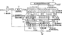
Figure 10 represents the block structure as the STBD of reference example of the present invention.
External clock EXTCLK input is had in the receiver (input buffer) 11 of retardation Trc.The clock CLKSTIN that receiver 11 outputs have the Trc time lag to external clock EXTCLK.
Clock CLKSTIN imported delay monitor 12 with retardation (Trc+Tdr), control pulse generation circuit 13 respectively and constitute reverse impulse with N revertive delay unit 16-1,16-2 of lag line 16 ... 16-n ... among the 16-N.
Postpone monitor 12 according to clock CLKSTIN output direct impulse FCLIN.Control pulse generation circuit is according to clock CLKSTIN output control pulse P, bP.
N forward delay cell 14-1,14-2 of gating pulse P, bP control formation direct impulse usefulness lag line 14 ... 14-n ... the action of 14-N.That is, by gating pulse P, bP determine direct impulse FCLIN whether direct impulse with lag line in transmission (whether monitoring external clock EXTCLK).
State retaining part control circuit 19 generates gating pulse BPM according to gating pulse Bp with from reverse impulse with the reverse impulse STCLK of lag line 16 output.Gating pulse BPM determines to carry out the timing (or reseting period) that state retaining part 15 resets.
The instantiation of simple declaration control pulse generation circuit here, 13 and state retaining part control circuit 19.
Figure 15 represents an example of control pulse generation circuit 13.
Control pulse generation circuit 13 is made of the known pulse generating circuit that phase inverter and NAND circuit constitute.The output signal of NAND circuit becomes gating pulse bP, when coming the level of reverse this gating pulse bP by phase inverter, and controlled pulse P.This control pulse generation circuit 13 afterwards, is exported gating pulse P, the bP of certain width when clock CLKSTIN becomes H by L.
Figure 16 represents an example of state retaining part control circuit 19.
State retaining part control circuit 19 comprises that supervision gating pulse bP becomes the moment and the flip-flop circuit in clock STCLK becomes L from H the moment (from the moment of reverse impulse with the real edge of lag line output reverse impulse) and the known pulse generating circuit that is made of phase inverter and NAND circuit of H from L.
Become the moment later the moment of L from H at the moment that becomes H from gating pulse bP from L and clock STCLK and begin through after certain time delay, 19 outputs of state retaining part control circuit have the gating pulse BPM of certain width.
That is, under the late situation of the moment of rising than gating pulse bP in the moment that clock STCLK descends, descending from clock STCLK begins through after certain time delay output control pulse BPM.In addition, the moment that clock STCLK descends be present in gating pulse bP be L during under the situation of (bP rise before), rise from gating pulse bP beginning to pass through certain time delay after, output control pulse BPM.
This reference example is to have state retaining part control circuit 19 with the difference of existing example (Fig. 1).
Direct impulse FCLIN is imposed on direct impulse lag line 14.Direct impulse with lag line 14 by the N that is connected in series forward delay cell 14-1, a 14-2 ... 14-n ... 14-N constitutes.Wherein, N and n are positive number, and n<N.
Gating pulse (direct impulse transmission of control signals) P, bP control N forward delay cell 14-1,14-2 ... 14-n ... the action of 14-N.When N forward delay cell 14-1,14-2 ... 14-n ... when 14-N was in operating state (can transmit the state of direct impulse), the direct impulse that each forward delay cell will receive from the forward delay cell of prime was transferred to the forward delay cell of back level.
The instantiation of direct impulse with the forward delay cell 14-n in the lag line 14 is described here.
Figure 11 represents the example of forward delay cell 14-n.
In this example, forward delay cell 14-n is made of three phase inverter I1, I2, I3 and two timing phase inverter CI1, CI2.The regularly action of phase inverter CI1, CI2 of gating pulse P, bP control.
At gating pulse P is the L level, and when gating pulse bP was the H level, regularly phase inverter CI1 became operating state, and regularly phase inverter CI2 becomes non-action status.Therefore, direct impulse FCLn-1 is transferred to the forward delay cell 14-(n-1) of back level through phase inverter CI1 regularly with regularly behind the phase inverter CI2.The output signal FFCLn of phase inverter I3 is imposed on state holding unit 15-n.
In addition, be the H level at gating pulse P, when gating pulse bP was the L level, regularly phase inverter CI1 became non-action status, and regularly phase inverter CI2 becomes operating state.Therefore, for all forward delay cell, the current potential VSS to timing phase inverter CI2 input L level is reset to the H level with node A.
Considered to set phase inverter I1, do not used output signal bFCLn with the symmetry of aftermentioned revertive delay unit 16-n (with reference to Figure 14).
The forward delay cell of input direct impulse changes the state (set/reset) of the state holding unit corresponding with it.Particularly, before direct impulse FCLIN input direct impulse is used lag line 14, all state holding unit 15-1,15-2 ... 15-n ... 15-N is in (R) state that resets, and becomes set (S) state corresponding to the state holding unit of forward delay cell of input direct impulse from (R) state that resets.
The result of change state holding unit 15-n state is the output signal FFCLn of forward delay cell.
N state holding unit 15-1,15-2 in the state retaining part 15 ... 15-n ... 15-N reverts to reset mode by gating pulse (state retaining part reset signal) BMP.State retaining part initializing circuit 17 is according to reset signal RESET output initializing signal bRSINI, force with N state holding unit 15-1,15-2 ... 15-n ... the state of 15-N is initialized as reset mode.
Here, simple declaration state holding unit 15-n and state retaining part initializing circuit 17.
Figure 12 represents the example of state holding unit 15-n.
State holding unit 15-n comprises the P channel MOS transistor P1, the P2 that are connected in series between power supply terminal VDD and the node C, be connected in series in N-channel MOS transistor N1, N2 between ground terminal VSS and the node C, be connected in the P channel MOS transistor P3 between power supply terminal VDD and the node C and be connected latch circuit LATCH between node C, the D.
In this example, latch circuit LATCH is not limited to be reset, and can be the static latch circuit that keeps equal state usually.When resetting, BPM and bRCLn-2 become the L level, and node C becomes the H level, and node D becomes the L level.BRCLn-2 is the signal from revertive delay described later unit 16-(n-2) output.
When gating pulse BPM is the H level, to forward delay cell 14-n input direct impulse FCLn-1, then the output signal FFCLn of forward delay cell 14-n becomes the H level, so state holding unit 15-n becomes SM set mode, that is, node C becomes the state that L level, node D become the H level.
Respectively the signal bQn of the node C of state holding unit 15-n and the signal Qn of node D are offered revertive delay described later unit 16-n.Control the action of revertive delay unit 16-n by output signal Qn, the bQn of state holding unit 15-n.
Figure 13 represents an example of state retaining part initializing circuit 17.
State retaining part initializing circuit 17 for example is made of the delay circuit that three phase inverters that are connected in series constitute.When reset signal RESET became the H level, control signal bRSINI became the L level, so the P channel MOS transistor P3 of Figure 12 becomes conducting state, state holding unit 15-n becomes reset mode.
The homing action of the homing action of gating pulse BPM and control signal bRSINI is distinguished as respective action.
Above-mentioned delay monitor 12, control pulse generation circuit 13, direct impulse are to monitor the synchronously required delay time T of external clock EXTCLK and internal clocking INTCLK-(Trc+Tdr) with the purpose of lag line 14, state retaining part 15 and state retaining part initializing circuit 17.
Relative with it, reverse impulse is correctly to duplicate the delay time T of monitor circuit monitors-(Trc+Tdr) with the purpose of lag line 16.Because reverse impulse is correct replica delay time τ-(Trc+Tdr) with the purpose of lag line 16, so copy direct impulse fully with lag line 14.That is, be symmetrical in hold mode portion 15 and dispose direct impulse lag line 14 and reverse impulse lag line 16, and two circuit structures are identical.
Reverse impulse with lag line 16 by the N that is connected in series revertive delay unit 16-1, a 16-2 ... 16-n ... 16-N constitutes.Reverse impulse with lag line 16 according to N state holding unit 15-1,15-2 in the state retaining part 15 ... 15-n ... the state of 15-N and CLKSTIN, at correct replica delay time τ-(Trc+Tdr) afterwards, export clock STCLK.
Here, the instantiation of reverse impulse with the revertive delay unit 16-n in the lag line 16 is described.
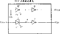
Figure 14 represents the example of revertive delay unit 16-n.
In this example, revertive delay unit 16-(n-1) is made of three phase inverter I4, I5, I6 and two timing phase inverter CI3, CI4.The regularly action of phase inverter CI3, CI4 of control signal Qn, bQn control from state holding unit 15-n output.
Corresponding to the revertive delay unit of the state holding unit of reset mode (the state holding unit after the regulation level), be that control signal Qn is that L level, control signal bQn are in the revertive delay unit of H level, regularly phase inverter CI4 becomes operating state, and regularly phase inverter CI3 becomes non-action status.Therefore, (=CLKSTIN) incoming timing phase inverter CI4 generates reverse impulse with clock RCLIN.
Corresponding to the revertive delay unit of the state holding unit of SM set mode (the state holding unit before the regulation level), be that control signal Qn is that H level, control signal bQn are in the revertive delay unit of L level, regularly phase inverter CI3 becomes operating state, and regularly phase inverter CI4 becomes non-action status.Therefore, the reverse impulse RCLn+1 of the revertive delay unit of prime generation is as the revertive delay unit of RCLn through level after regularly phase inverter CI3 and phase inverter I5 are transferred to.Apply the output signal bRCLn of phase inverter I6 to state holding unit 15-(n-2).
Consider to design phase inverter I4, so do not use its output signal RRCLn with the symmetry of forward delay cell 14-n (with reference to Figure 11).
When clock STCLK process has the driver 18 of retardation Tdr, become the internal clocking INTCLK synchronous with external clock EXTCLK.
Compare the clock synchronization circuit of this reference example (Figure 10) and the clock synchronization circuit of conventional example (Fig. 1), the former controls homing action by gating pulse BPM, and on the contrary, the latter controls homing action by gating pulse bP.
Under the situation of controlling homing action by gating pulse bP (under the situation of Fig. 1), reseting period (bP=L during) is irrelevant with reverse impulse, and only by the rising edge decision of clock CLKSTIN.At reseting period, the revertive delay unit of the input reverse impulse that resets, to be RCLi (i is a progression) be the state of level state holding unit behind two of the unit of H.
For example, in Fig. 1, under the situation in the forward position of revertive delay unit 16-(n-2) input reverse impulse, after two of this revertive delay unit 16-(n-2) level state holding unit 15-n and also lean on than this unit after state holding unit 15-(n+1) ... become reset mode.
But, in this case, at reseting period, the state of level state holding unit behind two of revertive delay unit of the input reverse impulse that resets usually.
Therefore, for example shown in Figure 17, in the timing of reverse impulse with existence two reverse impulse B1, B2 in the lag line 16, the reset state of level state holding unit (dotting) 15-3 behind two of revertive delay unit 16-1 of the last reverse impulse B1 of input, the disconnected reverse impulse of TURP with the part of lag line 16, be the reverse impulse usefulness lag line 16 among the revertive delay unit 16-2.
As a result, block the transmission path of back one reverse impulse B2 midway, the output of reverse impulse regularly disorderly, can not be carried out correct synchro control.
On the contrary, under the situation of controlling homing action by gating pulse BPM (under the situation of Figure 10), according to determining reseting period (BPM=L during) with the rising edge (or rising edge of gating pulse bP) of the negative edge of reverse impulse (clock) STCLK of lag line 16 output and clock CLKSTIN from reverse impulse.
That is, from the circuit diagram of Figure 16 as can be known, reseting period be from reverse impulse (clock) STCLK descend constantly and gating pulse bP rise constantly the later moment begin through after certain time delay necessarily during (BPM=L during).Wherein, reverse impulse (clock) STCLK descends constantly more late than gating pulse bP decline usually constantly.
In reseting period, the revertive delay unit of the input reverse impulse that resets, to be RCLi (i is a progression) be the state of level state holding unit behind two of the unit of H.
Here, under the situation of Figure 10, for the timing of reverse impulse with existence two reverse impulse B1, B2 in the lag line 16, usually last reverse impulse B1 (back edge) fully from reverse impulse with lag line 16 outputs after, carry out the homing action of state holding unit, so can not block reverse impulse halfway with the part of lag line 16, the i.e. back transmission path of a reverse impulse B2.
For example shown in Figure 180, last reverse impulse B1 (back edge) fully from reverse impulse with lag line 16 outputs after, carry out homing action, so when resetting, after two of the revertive delay unit 16-n of input back one reverse impulse B2 level state holding unit 15-(n+2) and thereafter back level unit 15-(n+3) ... state become reset mode.
Therefore, under the situation of Figure 10,,, can carry out correct synchro control so the output of reverse impulse regularly can be not random because can not block the transmission path of back one reverse impulse B2 halfway.
Therefore, in this reference example, consider the situation of reverse impulse with two reverse impulses of existence in the lag line 16, new design point retaining part control circuit 19, use this state retaining part control circuit 19, usually after reverse impulse is exported with lag line 16 from reverse impulse, carry out the homing action of state retaining part 15.
But, in the clock synchronization circuit of Figure 10, because according to determining reseting period with the moment of lag line 16 output reverse impulses (back edge), so produce resetting constantly in one-period because of changing phenomenon with moment of lag line 16 output reverse impulses (back edge) in each cycle variation from reverse impulse from reverse impulse.
In addition, be engraved in each when resetting when changing, the pulse width of the reverse impulse that produces in the state holding unit number (progression resets) that resets and one-period is variation thereupon also in cycle.
The variation of this progression that resets or the pulse width variation of reverse impulse have produced the increase of the current sinking that the difference of the internal clocking INTCLK that irregular action causes, the above unit of necessary amount that resets causes etc.
Specify this problem.
Figure 19 represents the waveform about the clock synchronization circuit homing action of Figure 10.Figure 20 to Figure 27 represents the state of each clock synchronization circuit constantly of Figure 19 waveform.
The situation (cycle 2) that the decline of STCLK is constantly more late than the rising of bP constantly
At first, in the cycle 2, when clock CLKSTIN rises (L → H), according to state holding unit 15-1, the 15-2 of state retaining part 15 ... 15-n ... the state of 15-N (set/reset) forms the forward position (constantly 1. and Figure 20) of reverse impulse B2.
Promptly, in this example, in the moment that clock CLKSTIN rises, n level state holding unit 15-n and its prime state holding unit 15-1 ..., 15-(n-1) become SM set mode (bQi (i is a progression)=L), n+1 level state holding unit 15-(n+1) and thereafter level state holding unit 15-(n+2) ..., 15-N becomes reset mode (bQi (i is a progression)=H) is so receive the forward position of the n level revertive delay unit 16-n of bQn according to clock CLKSTIN formation reverse impulse B2.
Afterwards, reverse impulse (forward position) B2 to revertive delay unit 16-1 (reverse impulse with the output terminal of lag line) transmit successively revertive delay unit 16-(n-1), 16-(n-2) ....
On the other hand, when moment CLKSTIN rises, respond this rising, control pulse generation circuit 13 generation gating pulse bP (=L).
In this example, output control pulse bP (=L) during, so the reverse impulse B1 that generates the cycles 1 before 16 output cycles 2 with lag line from reverse impulse (back edge) not is state retaining part control circuit 19 output control pulse BPM not.
Afterwards, the reverse impulse B1 that generates 16 output cycles 1 with lag line from reverse impulse (back edge), when STCLK (=RCL1) when H becomes L, state retaining part control circuit 19 begins (=L) (constantly 2. and Figure 21) through output control pulse BPM after certain time delay when changing.
When gating pulse BPM becomes L, at this constantly, the revertive delay unit (the revertive delay unit that the forward position of reverse impulse B2 exists and revertive delay unit thereafter) that exists of the reverse impulse B2 that resets, be the state of grade state holding unit behind two of RCLi (i is a progression) the revertive delay unit that becomes H (bRCi is L).
For example, in this example, become the moment of L at gating pulse BPM, n-7 level and revertive delay unit 16-(n-7) afterwards ... 16-n ... the output signal RCLn-7 of 16-N ... RCLn ... become H, thus the state holding unit 15-(n-5) from the n-5 level of level behind two of n-7 to the n level ... 15-n become simultaneously reset mode (bQn-5 ... bQn=H).
N+1 and state holding unit 15-(n+1) thereafter ... be generally reset mode.
In addition, gating pulse BPM be L during (reseting period), reverse impulse B2 (forward position) successively to its output terminal transmission reverse impulse with lag line 16.Therefore, gating pulse BPM be L during, the state holding unit of level after two of the revertive delay unit of the input reverse impulse B2 that resets successively (forward position) (during 3. and Figure 22).
For example, in this example, gating pulse BPM be L during, to revertive delay unit 16-(n-8), 16-(n-9) input reverse impulse B2 (forward position).Therefore, output signal RCLn-8, the RCLn-9 of revertive delay unit 16-(n-8), 16-(n-9) become H successively, the state (bQn-6, bQn-7=H) of the state holding unit of reset successively n-6 level and n-7 level.
Therefore, in the cycle 2,8 state holding unit 15-n from n to the n-7 level ... 15-(n-7) becomes reset mode from SM set mode.
Afterwards, when clock CLKSTIN descends (H → L), according to state holding unit 15-1, the 15-2 of state retaining part 15 ... 15-n ... the state of 15-N (set/reset) forms the back edge (constantly 4. and Figure 23) of reverse impulse B2.
Promptly, in this example, in the moment that clock CLKSTIN descends, n-8 level state holding unit 15-(n-8) and its prime state holding unit 15-1 ... 15-(n-9) become SM set mode (bQi (i is a progression)=L), n-7 level state holding unit 15-(n-7) and thereafter level state holding unit 15-(n-6) ... 15-N becomes reset mode, and (bQi (i is a progression)=H) is so receive the n-8 level revertive delay unit 16-(n-8) of bQn-7 forms reverse impulse B2 according to clock CLKSTIN back edge.
In the cycle 2, form the back edge of reverse impulse B2 with the n-8 level revertive delay unit 16-(n-8) of lag line 16 output terminals near reverse impulse.Therefore, the pulse width of reverse impulse B2 narrows down.
Afterwards, reverse impulse B2 (back along) successively to revertive delay unit 16-1 (reverse impulse with the output terminal of lag line) transmission revertive delay unit 16-(n-9), 16-(n-10) ....
Thus, in the decline of STCLK constantly than the rising of bP under the constantly late situation, state retaining part control circuit 19 delay voltage (affirmation) regularly that resets from the action of reverse impulse with lag line 16 output reverse impulse B1, so from then on increased the progression of reverse impulse B2 transmission reverse impulse with lag line 16, the result, the progression that resets of state holding unit increases, and the pulse width of reverse impulse B2 narrows down.
As mentioned above, the generation of the reverse impulse B2 in the cycle 2 that is through with before, is beginning to generate reverse impulse B3 in the cycle 3 after the cycle 2 from reverse impulse with lag line 16 output reverse impulse B2 (back edge).
Be engraved in during the decline of STCLK bP=L during in situation (cycle 3)
At first, in the cycle 3, when clock CLKSTIN rises (L → H), according to state holding unit 15-1, the 15-2 of state retaining part 15 ... 15-n ... the state of 15-N (set/reset) form reverse impulse B2 the forward position (1. constantly ' and Figure 24).
Promptly, in this example, in the moment that clock CLKSTIN rises, n level state holding unit 15-n and its prime state holding unit 15-1 ..., 15-(n-1) become SM set mode (bQi (i is a progression)=L), n+1 level state holding unit 15-(n+1) and thereafter level state holding unit 15-(n+2) ..., 15-N becomes reset mode (bQi (i is a progression)=H) is so receive the forward position of the n level revertive delay unit 16-n of bQn according to clock CLKSTIN formation reverse impulse B3.
Afterwards, reverse impulse (forward position) B3 to revertive delay unit 16-1 (reverse impulse with the output terminal of lag line) transmit successively revertive delay unit 16-(n-1), 16-(n-2) ....
On the other hand, when moment CLKSTIN rises, respond this rising, control pulse generation circuit 13 generation gating pulse bP (=L).
In this example, output control pulse bP (=L) during, not the reverse impulse B2 that generates the cycles 2 before 16 output cycles 3 with lag line from reverse impulse (back edge) (2. constantly ' and Figure 25), so state retaining part control circuit 19 from gating pulse bP by L become H begin through output control pulse BPM after certain time delay (=L).
When gating pulse BPM becomes L, at this constantly, the revertive delay unit (the revertive delay unit that the forward position of reverse impulse B43 exists and revertive delay unit thereafter) that exists of the reverse impulse B3 that resets, be the state of grade state holding unit behind two of RCLi (i is a progression) the revertive delay unit that becomes H (bRCi is L).
For example, in this example, become the moment of L at gating pulse BPM, n-1 level and afterwards revertive delay unit 16-(n-1), 16-n ... the output signal RCLn-1 of 16-N, RCLn ... become H, thus the state holding unit 15-(n+1) from the n+1 level of level behind two of n-1 to the N level ... 15-N become reset mode (bQn+1 ... bQn=H).
In this example, n+1 and state holding unit 15-(n+1) thereafter ... be generally reset mode.
In addition, gating pulse BPM be L during (reseting period), reverse impulse B3 (forward position) successively to its output terminal transmission reverse impulse with lag line 16.Therefore, gating pulse BPM be L during, the state holding unit of level after two of the revertive delay unit of the input reverse impulse B3 that resets successively (forward position) (during 3. ' and Figure 26).
For example, in this example, gating pulse BPM be L during, to revertive delay unit 16-(n-2), 16-(n-3) input reverse impulse B3 (forward position).Therefore, output signal RCLn-2, the RCLn-3 of revertive delay unit 16-(n-2), 16-(n-3) become H successively, the state (bQn, bQn-1=H) of the state holding unit of reset successively n and n-1.
Therefore, in the cycle 3,2 state holding unit 15-n, 15-(n-1) from n to the n-1 level become reset mode from SM set mode.
Afterwards, when clock CLKSTIN descends (H → L), according to state holding unit 15-1, the 15-2 of state retaining part 15 ... 15-n ... the state of 15-N (set/reset), form reverse impulse B3 back edge (4. constantly ' and Figure 27).
Promptly, in this example, in the moment that clock CLKSTIN descends, n-2 level state holding unit 15-(n-2) and its prime state holding unit 15-1 ... 15-(n-3) become SM set mode (bQi (i is a progression)=L), n-1 level state holding unit 15-(n-1) and thereafter level state holding unit 15-n ... 15-N becomes reset mode, and (bQi (i is a progression)=H) is so receive the n level revertive delay unit 16-(n-2) of bQn-1 forms reverse impulse B3 according to clock CLKSTIN back edge.
In the cycle 3, form the back edge of reverse impulse B3 with the n-2 level revertive delay unit 16-(n-2) of lag line 16 output terminals away from reverse impulse.Therefore, the pulse width of reverse impulse B3 broadens.
Afterwards, reverse impulse B3 (back along) successively to revertive delay unit 16-1 (reverse impulse with the output terminal of lag line) transmission revertive delay unit 16-(n-3), 16-(n-4) ....
Thus, the decline of STCLK be present in constantly bP be L during in situation under, state retaining part control circuit 19 delay voltage regularly (affirmation) that do not reset from the action of reverse impulse with lag line 16 output reverse impulse B2.So from then on reduced the progression of reverse impulse B3 transmission reverse impulse with lag line 16, the result, the progression that resets of state holding unit reduces, and the pulse width of reverse impulse B3 broadens.
As mentioned above, the generation of the reverse impulse B3 in the cycle 3 that is through with before, is beginning to generate reverse impulse B4 in the cycle 4 after the cycle 3 from reverse impulse with lag line 16 output reverse impulse B3 (back edge).
The action that generates reverse impulse B4 in cycle 4 is identical with the action of generation reverse impulse B2 in the cycle 2.
The homing action of the clock synchronization circuit of Figure 10 has been described above, but in this clock synchronization circuit, constantly late situation (the wide situation of pulse width that last reverse arteries and veins is burst) is risen in the decline of STCLK constantly than bP under, delay voltage regularly (determining from the action of reverse impulse with lag line output reverse impulse) resets, from then on increased the progression of reverse impulse transmission reverse impulse with lag line, the result, the progression that resets of state holding unit increases, and the pulse width of reverse impulse narrows down.
On the other hand, the decline of STCLK be present in constantly bP be L during in situation (the narrow situation of pulse width that last reverse arteries and veins is burst) under, delay voltage does not regularly reset, from then on reduced the progression of reverse impulse B3 transmission reverse impulse with lag line, the result, the progression that resets of state holding unit reduces, and the pulse width of reverse impulse broadens.
Thus, in the clock synchronization circuit of Figure 10, so the pulse width difference of the order of magnitude of the state holding unit that resets in each cycle (progression resets) or reverse impulse is owing to irregular action produces the difference of internal clocking INTCLK and the problem that current sinking increases.
In the following embodiments, the quantity (progression resets) of the state holding unit that resets and the always constant clock synchronization circuit of pulse width of reverse impulse are described.
Figure 28 represents the block structure as the STBD of the embodiment of the invention 1.
External clock EXTCLK input is had in the receiver (input buffer) 11 of retardation Trc.The clock CLKSTIN that receiver 11 outputs have the Trc time lag to external clock EXTCLK.
Clock CLKSTIN imported delay monitor 12 with retardation (Trc+Tdr), control pulse generation circuit 13 respectively and constitute reverse impulse with N revertive delay unit 16-1,16-2 of lag line 16 ... 16-n ... among the 16-N.
Postpone monitor 12 according to clock CLKSTIN output direct impulse FCLIN.Control pulse generation circuit is according to clock CLKSTIN output control pulse P, bP, bP2.
N forward delay cell 14-1,14-2 of gating pulse P, bP control formation direct impulse usefulness lag line 14 ... 14-n ... the action of 14-N.That is, by gating pulse P, bP determine direct impulse FCLIN whether direct impulse with lag line 14 in transmission (whether monitoring external clock EXTCLK).
In addition, gating pulse bP2 determines to carry out the timing that resets (or reseting period) of state retaining part 15.
The instantiation of simple declaration control pulse generation circuit here, 13.
Figure 33 represents an example of control pulse generation circuit 13.
Control pulse generation circuit 13 is made of the known pulse generating circuit that phase inverter and NAND circuit constitute.The output signal of NAND circuit becomes gating pulse bP, when coming the level of reverse this gating pulse bP by phase inverter, and controlled pulse P.Gating pulse bP becomes gating pulse bP2 during via the even number of inverters that is connected in series (delay circuit with X time delay).
This control pulse generation circuit 13 is exported gating pulse bP, the bP2 of the certain width that Y determines by time delay (be L during be Y) respectively and by the gating pulse P of certain width that time delay, Y determined (be H during be Y) when clock CLKSTIN becomes H by L.
In addition, the STBD of present embodiment is different with above-mentioned reference example, does not have state retaining part control circuit (with reference to Figure 10).That is, whether do not monitor the back edge of the reverse impulse that generates the previous cycle with lag line 16 output current periods from reverse impulse.
This is because present embodiment STBD does not carry out resetting of state retaining part 15 according to reverse impulse.Promptly, suppose that reverse impulse is with there being two reverse impulses in the lag line 16, owing to be not according to reverse impulse but according to the state (set/reset) of back level state holding unit reset (this point is important), so in the STBD of present embodiment, do not produce the problem of reverse impulse lag line 16 broken strings.
Therefore, the STBD of present embodiment does not need to possess the state retaining part control circuit (by gating pulse bP2 come the resetting of state of a control retaining part 15) of supervision reverse impulse with the output signal STCLK of lag line 16, therefore can dwindle the area of STBD.
Direct impulse FCLIN is imposed on direct impulse lag line 14.Direct impulse with lag line 14 by the N that is connected in series forward delay cell 14-1, a 14-2 ... 14-n ... 14-N constitutes.Wherein, N and n are positive number, and n<N.
Gating pulse (direct impulse transmission of control signals) P, bP control N forward delay cell 14-1,14-2 ... 14-n ... the action of 14-N.When N forward delay cell 14-1,14-2 ... 14-n ... when 14-N was in operating state (can transmit the state of direct impulse), the direct impulse that each forward delay cell will receive from the forward delay cell of prime was transferred to the forward delay cell of back level.
The instantiation of direct impulse with the forward delay cell 14-n in the lag line 14 is described here.
Figure 29 represents the example of forward delay cell 14-n.
In this example, forward delay cell 14-n is made of two phase inverter I2, I3 and two timing phase inverter CI1, CI2.The regularly action of phase inverter CI1, CI2 of gating pulse P, bP control.
At gating pulse P is the L level, and when gating pulse bP was the H level, regularly phase inverter CI1 became operating state, and regularly phase inverter CI2 becomes non-action status.Therefore, direct impulse FCLn-1 is transferred to the forward delay cell 14-(n-1) of back level through phase inverter CI1 regularly with regularly behind the phase inverter CI2.The output signal FFCLn of phase inverter I3 is imposed on state holding unit 15-n.
In addition, be the H level at gating pulse P, when gating pulse bP was the L level, regularly phase inverter CI1 became non-action status, and regularly phase inverter CI2 becomes operating state.Therefore, for all forward delay cell, the current potential VSS to timing phase inverter CI2 input L level is reset to the H level with node A.
In addition, the forward delay cell 14-n of the STBD of present embodiment is different with above-mentioned reference example, does not have phase inverter I1 (with reference to Figure 11).This is because present embodiment STBD does not carry out resetting of state retaining part 15 according to reverse impulse.
That is, because do not carry out resetting of state retaining part 15, so in the STBD of present embodiment, revertive delay pulse described later (with reference to Figure 32) does not have phase inverter I6 (with reference to Figure 14) according to reverse impulse.
Therefore, because the symmetry of forward delay cell and revertive delay unit, so forward delay cell 14-n does not have phase inverter I1 (with reference to Figure 11) yet.Therefore, in the STBD of present embodiment, the area of forward delay cell 14-n has only dwindled the part of a phase inverter.
The forward delay cell of input direct impulse changes the state (set/reset) of the state holding unit corresponding with it.Particularly, the state holding unit corresponding to the forward delay cell of importing direct impulse becomes set (S) state from (R) state that resets.
Wherein, after second round, as described later, only the variation δ part by the transmission of direct impulse at least progression just is enough to carry out resetting of state retaining part 15, becomes SM set mode so only be in the unit of reset mode in the state holding unit corresponding to the forward delay cell of input direct impulse.
The result of change state holding unit 15-n state is the output signal FFCLn of forward delay cell.
N state holding unit 15-1,15-2 in the state retaining part 15 ... 15-n ... 15-N reverts to reset mode according to the output signal of gating pulse (state retaining part reset signal) Bp2 and back level state holding unit.
That is, at first, determine reseting period by gating pulse Bp2.In this reseting period, carry out resetting of state retaining part 15.In reseting period, when the output signal Qn+1 of the back level state holding unit 15-(n-1) of state holding unit 15-n was L, the state of state holding unit 15-n became reset mode.
In STBD, direct impulse monitors retardation τ-(Trc+Tdr) with lag line 14 after, usually the boundary that in state retaining part 15, has SM set mode and reset mode, and this boundary makes the state holding unit of preceding-stage side all become SM set mode, makes the state holding unit of rear-stage side all become reset mode.
In the present embodiment, at reseting period, prime state holding unit is that the state holding unit of the SM set mode of reset mode makes its state become reset mode from SM set mode.At this moment, the state holding unit of SM set mode begins to be changed to successively reset mode (transmission that resets) from the state holding unit that is positioned at border.
The quantity of the state holding unit that resets (progression resets) is determined by the width of gating pulse bP2 (bP2=L during).In addition, the progression that resets must transmit the variation δ of progression greater than direct impulse.
In the STBD of present embodiment, the transmission that irrespectively resets with the transmission of reverse impulse.At this moment, when the transmission speed of the transmission speed ratio inverse pulse that resets was fast, reverse impulse can not correctly duplicate τ-(Trc+Tdr) with lag line 16.
Make gating pulse bP only postpone certain time delay, generate gating pulse bP2, the resetting of this gating pulse bP2 state of a control retaining part 15.That is, make the period that resets fully more late than the period that forms the reverse impulse forward position, the transmission that resets usually can not caught up with and not surpassed the transmission of reverse impulse.
State retaining part initializing circuit 17 is according to reset signal RESET output initializing signal bRSINI, force with N state holding unit 15-1,15-2 ... 15-n ... the state of 15-N is initialized as reset mode.
Here, simple declaration state holding unit 15-n and state retaining part initializing circuit 17.
Figure 30 represents the example of state holding unit 15-n.
State holding unit 15-n comprises the P channel MOS transistor P1, the P2 that are connected in series between power supply terminal VDD and the node C, be connected in series in N-channel MOS transistor N1, N2 between ground terminal VSS and the node C, be connected in the P channel MOS transistor P3 between power supply terminal VDD and the node C and be connected latch circuit LATCH between node C, the D.
In this example, latch circuit LATCH is not limited to be reset, and can be the static latch circuit that keeps equal state usually.When resetting, bP2 and Qn+1 become the L level, and node C becomes the H level, and node D becomes the L level.
BP2 is the signal from control pulse generation circuit 13 outputs, and Qn+1 is the signal from back level state holding unit 15-(n+1) output.In the STBD of present embodiment, replace from the signal bRCLn-2 of revertive delay unit 16-(n-2) output, control by a signal Qn+1 and reset from back level state holding unit 15-(n+1) output.
When gating pulse bP2 is the H level, to forward delay cell 14-n input direct impulse FCLn-1, then the output signal FFCLn of forward delay cell 14-n becomes the H level, so state holding unit 15-n becomes SM set mode, that is, node C becomes the state that L level, node D become the H level.
Respectively the signal bQn of the node C of state holding unit 15-n and the signal Qn of node D are offered revertive delay described later unit 16-n.Control the action of revertive delay unit 16-n by output signal Qn, the bQn of state holding unit 15-n.
When gating pulse bP2 was the L level, when the state holding unit 15-(n+1) of back level was reset mode (Qn+1=L), state holding unit 15-n became reset mode, that is, node C becomes the state that H level, node D become the L level.
The signal Qn of the node D of state holding unit 15-n is offered the state holding unit 15-(n-1) of prime.When the state holding unit 15-(n-1) of prime receive Qn (=L) time, if reseting period (bP2=L), then this state becomes reset mode.
Figure 31 represents an example of state retaining part initializing circuit 17.
State retaining part initializing circuit 17 for example is made of the delay circuit that three phase inverters that are connected in series constitute.When reset signal RESET became the H level, control signal bRSINI became the L level, so the P channel MOS transistor P3 of Figure 30 becomes conducting state, state holding unit 15-n becomes reset mode.
The homing action of the homing action of gating pulse bP2 and control signal bRSINI is distinguished as respective action.
Above-mentioned delay monitor 12, control pulse generation circuit 13, direct impulse are to monitor the synchronously required delay time T of external clock EXTCLK and internal clocking INTCLK-(Trc+Tdr) with the purpose of lag line 14, state retaining part 15 and state retaining part initializing circuit 17 (they are referred to as monitoring circuit).
Relative with it, reverse impulse is correctly to duplicate the delay time T of monitor circuit monitors-(Trc+Tdr) with the purpose of lag line 16.Because reverse impulse is correct replica delay time τ-(Trc+Tdr) with the purpose of lag line 16, so copy direct impulse fully with lag line 14.That is, be symmetrical in hold mode portion 15 and dispose direct impulse lag line 14 and reverse impulse lag line 16, and two circuit structures are identical.
Reverse impulse with lag line 16 by the N that is connected in series revertive delay unit 16-1, a 16-2 ... 16-n ... 16-N constitutes.Reverse impulse with lag line 16 according to N state holding unit 15-1,15-2 in the state retaining part 15 ... 15-n ... the state of 15-N and CLKSTIN, at correct replica delay time τ-(Trc+Tdr) afterwards, export clock STCLK.
Here, the instantiation of reverse impulse with the revertive delay unit 16-n in the lag line 16 is described.
Figure 32 represents the example of revertive delay unit 16-n.
In this example, revertive delay unit 16-(n-1) is made of two phase inverter I4, I5 and two timing phase inverter CI3, CI4.The regularly action of phase inverter CI3, CI4 of control signal Qn, bQn control from state holding unit 15-n output.
Corresponding to the revertive delay unit of the state holding unit of reset mode (the state holding unit after the regulation level), be that control signal Qn is that L level, control signal bQn are in the revertive delay unit of H level, regularly phase inverter CI4 becomes operating state, and regularly phase inverter CI3 becomes non-action status.Therefore, (=CLKSTIN) incoming timing phase inverter CI4 generates reverse impulse with clock RCLIN.
Corresponding to the revertive delay unit of the state holding unit of SM set mode (the state holding unit before the regulation level), be that control signal Qn is that H level, control signal bQn are in the revertive delay unit of L level, regularly phase inverter CI3 becomes operating state, and regularly phase inverter CI4 becomes non-action status.Therefore, the reverse impulse RCLn+1 of the revertive delay unit of prime generation is as the revertive delay unit of RCLn through level after regularly phase inverter CI3 and phase inverter I5 are transferred to.
In addition, revertive delay unit 16-(n-1) of the STBD of present embodiment is different with above-mentioned reference example, does not have phase inverter I6 (with reference to Figure 14).This is because the STBD of present embodiment does not carry out resetting of state retaining part 15 according to reverse impulse.
Therefore, in the STBD of present embodiment, the area of revertive delay unit 16-n only dwindles a phase inverter part.
Consider to design phase inverter I4, so do not use its output signal RRCLn-1 with the symmetry of forward delay cell 14-n (with reference to Figure 29).
When clock STCLK process has the driver 18 of retardation Tdr, become the internal clocking INTCLK synchronous with external clock EXTCLK.
Compare the clock synchronization circuit (Figure 28) of present embodiment and the clock synchronization circuit (Figure 10) of reference example, the very big difference of the homing action of state holding unit 15-n is, the former controls homing action according to the set/reset state Qn+1 of gating pulse bP2 and back level state holding unit 15-(n+1), on the contrary, the latter controls homing action according to the output signal bRCLn-2 of the revertive delay unit 16-(n-2) of gating pulse BPM and two primes.
In existing example (Fig. 1), output signal bRCLn-2 according to the revertive delay unit 16-(n-2) of gating pulse bP and two primes controls homing action, at this moment, with existing in the timing (Figure 17) of two reverse impulse B1, B2 in the lag line 16, there be the problem of electric cut-out reverse impulse at reverse impulse with lag line 16.
In reference example (Figure 10),, the gating pulse bP that has example now is changed to gating pulse BPM in order to address this problem.At this moment, though solved the broken string problem of reverse impulse with lag line 16, but increase owing to new design point retaining part control circuit makes area simultaneously, and the pulse width difference of quantity of the state holding unit that resets in each cycle (progression resets) or reverse impulse has caused problems such as current sinking increase.
In the present invention (Figure 28), can prevent that reverse impulse from increasing with area in the broken string problem of lag line 16 and the reference example and the problem of consumed power increase.That is, in the present invention, do not need state retaining part control circuit, in the whole cycle, the pulse width of quantity of the state holding unit that resets (progression resets) or reverse impulse is always identical.
In the present invention, carry out homing action by new principle (detailed action described later), so may produce the transmission that reverse impulse is caught up with and surpassed in the transmission that resets.For this problem, can control homing action and solve easily by the gating pulse bP2 that passes through that reseting period is formed only postpone period certain hour from the forward position of reverse impulse, promptly only sends gating pulse bP within a certain period of time.
The following describes the action of the clock synchronization circuit of Figure 28 to Figure 33.
Figure 34 represents the waveform about the clock synchronization circuit homing action of Figure 28 to Figure 33.Figure 35 to Figure 37 represents the state of Figure 34 waveform at each clock synchronization circuit constantly.
At first, in the cycle 2, when clock CLKSTIN rises (L → H), according to state holding unit 15-1, the 15-2 of state retaining part 15 ... 15-n ... the state of 15-N (set/reset) forms the forward position (constantly 1. and Figure 35) of reverse impulse B2.
Promptly, in this example, in the moment that clock CLKSTIN rises, n level state holding unit 15-n and its prime state holding unit 15-1 ..., 15-(n-1) become SM set mode (bQi (i is a progression)=L), n+1 level state holding unit 15-(n+1) and thereafter level state holding unit 15-(n+2) ..., 15-N becomes reset mode (bQi (i is a progression)=H) is so receive the forward position of the n level revertive delay unit 16-n of bQn+1 according to clock CLKSTIN formation reverse impulse B2.
Afterwards, reverse impulse (forward position) B2 to revertive delay unit 16-1 (reverse impulse with the output terminal of lag line) transmit successively revertive delay unit 16-(n-1), 16-(n-2) ....
On the other hand, when moment CLKSTIN rises, respond this rising, control pulse generation circuit 13 generation gating pulse bP (=L).
In the present invention, the pulse width of gating pulse bP (bP=L during) is important.
That is, as described later, in the present invention, determine reseting period, determine the progression that resets by this reseting period by gating pulse bP (being actually bP2).Therefore, the pulse width of gating pulse bP must have the width of state holding unit of the progression of the variation δ (with reference to Fig. 8 and Fig. 9) that can be reset to the transmission progression that is equivalent to direct impulse less.
For this variation δ, must be by experiment or experience come prior confirmation.In addition, according to this variation δ determine for example to form Figure 33 time delay Y the quantity of phase inverter.
After generating gating pulse bP, if X time delay (X time delay of Figure 33) through stipulating then generates gating pulse bP2.This gating pulse bP2 is offered state retaining part 15 (constantly 2. and Figure 36).
Here, in the present invention, time delay, X also was a key factor.
That is, as mentioned above, when clock CLKSTIN rises, form the forward position (1. constantly) of reverse impulse B2.Wherein, in the forward position that forms reverse impulse B2, beginning reset mode retaining part 15, when the transmission speed of the transmission speed ratio inverse pulse that resets was fast, the transmission of reverse impulse was caught up with and surpassed in the transmission that resets.
In addition, even suppose that the transmission of the transmission speed ratio inverse pulse that resets is fast, the transmission of not catching up with and surpassing reverse impulse for the transmission that resets, (when gating pulse bP forms) is through after certain time delay when the forward position from reverse impulse B2 forms, generate reverse impulse B2, the resetting of initial state retaining part 15.
Gating pulse bP2 be L during in (reseting period), in the state retaining part 15, the transmission that irrespectively resets with the transmission of reverse impulse.
That is, at reseting period, the state holding unit of prime is that the state holding unit of the SM set mode of reset mode becomes reset mode from SM set mode.
For example, in this example, at gating pulse bP2 is the moment of L, state holding unit 15-1, the 15-2 from the 1st grade to the n level ... 15-n ... 15-n is a SM set mode, the state holding unit 15-(n+1) from the n+1 level to the N level ... 15-N becomes reset mode.
Therefore, at first, (state of=L) n level state holding unit 15-n becomes reset mode (bQn=H) from SM set mode (bQn=L) to receive back level state holding unit 15-(n+1) the output signal Qn+1 of gating pulse bP2 and reset mode.
Afterwards, receive gating pulse bP2 (=L) and the back level state holding unit 15-n output signal Qn of reset mode (state of=L) n-1 level state holding unit 15-(n-1) becomes reset mode (bQn-1=H) from SM set mode (bQn-1=L).
In this example, afterwards, bP2 becomes H, and reseting period finishes, so the progression that resets of state holding unit becomes 2 grades (state holding unit 15-(n-1), 15-n).
Thus, in the present invention, determine the progression that resets, do not rely on the position, forward position of reverse impulse, so in a plurality of cycles, the progression that resets usually equates (2 grades) by reseting period.In addition, as mentioned above, this progression that resets becomes and is equivalent to the progression of the transmission progression variation δ (with reference to Fig. 8 and Fig. 9) of direct impulse at least.
Therefore, whether needn't detect the back edge of the reverse impulse B1 that generates the previous cycle in 16 these cycles of output with lag line from reverse impulse, also need not state retaining part control circuit (with reference to Figure 10).
In addition, in a plurality of cycles, the progression that resets equates usually, and the pulse width of reverse impulse equates that also so can carry out unified action, consumed power is also very little.
Afterwards, when clock CLKSTIN descends (H → L), according to state holding unit 15-1, the 15-2 of state retaining part 15 ... 15-n ... 15-n ... the state of 15-N (set/reset) forms the back edge (constantly 3. and Figure 37) of reverse impulse B2.
Promptly, in this example, in the moment that clock CLKSTIN descends, the state holding unit 15-(n-2) of n-2 level and the state holding unit 15-3 of its prime ... 15-(n-9) becomes SM set mode (bQi (i is a progression)=L), the state holding unit 15-(n-1) of n-1 level and thereafter level state holding unit 15-n ... 15-N becomes reset mode, and (bQi (i is a progression)=H) is so receive the n-2 level revertive delay unit 16-(n-2) of bQn-1 forms reverse impulse B2 according to clock CLKSITN back edge (RCLi=L.Wherein, i be n-2, n-1 ... N).
Afterwards, reverse impulse B2 (back edge) transmits revertive delay unit 16-(n-3), 16-(n-10) successively to revertive delay unit 16-1 (reverse impulse with the output terminal of lag line).
By above action, the generation of the reverse impulse B2 of end period 2, but before, beginning to generate reverse impulse B3 in the cycle 3 after the cycle 2 with lag line 16 output reverse impulse B2 (back edge) from reverse impulse.
But the cycle 3 is also identical with the cycle 2, determines the progression that resets by reseting period, because do not rely on the position of reverse impulse B2, B3, so the progression that resets equates (2 grades).
As mentioned above, in homing action of the present invention, determine the progression that resets, because do not rely on the position in reverse impulse forward position, so in a plurality of cycles, the progression that resets equates usually by reseting period.In addition, this progression that resets is to be equivalent to the progression of the variation δ of direct impulse transmission progression at least.
Therefore, whether needn't detect from the back edge of reverse impulse with lag line output reverse impulse, also need not state retaining part control circuit (with reference to Figure 10), can dwindle the area of STBD.In addition, if the progression that resets is minimum value, promptly is equivalent to the progression of variation δ, then because the state holding unit that needn't reset too much, so current sinking is also very little.
In addition, for homing action, the timing that the sum of series that resets enforcement resets identical size of current sinking that means in each cycle is regularly all identical in each cycle with generation.
The generation of the power supply noise that current sinking causes is the synchronous reason of difference more or less in the synchronizing circuit.If the size of current sinking and generation are regularly irregular, then synchronous measures of dispersion difference is difficult to compensate synchronous difference.On the contrary, as shown in the present, if the size of current sinking and generation clocking discipline, then measures of dispersion is certain synchronously, compensates synchronous difference easily.
As a result, can realize the high accuracy clock synchronizing circuit.
In the present invention, carry out resetting of state holding unit according to the state of the state holding unit of back level, rather than carry out according to the position of reverse impulse.Therefore, gating pulse bP2 be L during (reseting period), irrespectively carry out the transmission that resets of state retaining part with the transmission of reverse impulse.
At this moment, with the formation in the forward position of reverse impulse resetting of initial state retaining part simultaneously, when the transmission speed of the transmission speed ratio inverse pulse that resets was fast, the transmission of reverse impulse was caught up with and surpassed in the transmission that resets.
In addition, even suppose that the transmission of the transmission speed ratio inverse pulse that resets is fast, the transmission of not catching up with and surpassing reverse impulse for the transmission that resets, when the forward position of reverse impulse forms (when gating pulse bP forms) through behind the certain time delay X, generate gating pulse bP2, the period that resets of delaying state retaining part.
The STBD of embodiment 2 is with a part combined form of the STBD of the foregoing description 1 (Figure 28) with existing STBD (Fig. 1).
That is, in the present invention, gating pulse bP2 be L during (reseting period), the reset transmission and irrelevant the carrying out of the transmission of reverse impulse of state retaining part.In the STBD of the foregoing description 1, only postpone the next corresponding problem of X time delay about this point by making reseting period.
In the present embodiment, append the condition that the position according to reverse impulse resets, then no matter the effect of the transmission of reverse impulse is not is not caught up with and surpassed in the transmission that all can obtain resetting under which kind of condition by STBD to embodiment 1.
Here, as the condition that resets, append the condition that in top-ranking's revertive delay unit, has reverse impulse for example (forward position), in the present invention, as other condition that resets, having the state holding unit of back level is the condition of reset mode, and existing problem (the reverse impulse broken string of lag line) does not then take place.
Figure 38 represents the block structure as the STBD of the embodiment of the invention 2.
External clock EXTCLK input is had in the receiver (input buffer) 11 of retardation Trc.The clock CLKSTIN that receiver 11 outputs have the Trc time lag to external clock EXTCLK.
Clock CLKSTIN imported delay monitor 12 with retardation (Trc+Tdr), control pulse generation circuit 13 respectively and constitute reverse impulse with N revertive delay unit 16-1,16-2 of lag line 16 ... 16-n ... among the 16-N.
Postpone monitor 12 according to clock CLKSTIN output direct impulse FCLIN.Control pulse generation circuit is according to clock CLKSTIN output control pulse P, bP, bP2.
N forward delay cell 14-1,14-2 of gating pulse P, bP control formation direct impulse usefulness lag line 14 ... 14-n ... the action of 14-N.That is, by gating pulse P, bP determine direct impulse FCLIN whether direct impulse with lag line 14 in transmission (whether monitoring external clock EXTCLK).
In addition, gating pulse bP2 determines to carry out the timing that resets (or reseting period) of state retaining part 15.
The instantiation of simple declaration control pulse generation circuit here, 13.
Figure 43 represents an example of control pulse generation circuit 13.
Control pulse generation circuit 13 is made of the known pulse generating circuit that phase inverter and NAND circuit constitute.The output signal of NAND circuit becomes gating pulse bP, when coming the level of reverse this gating pulse bP by phase inverter, and controlled pulse P.Gating pulse bP becomes gating pulse bP2 during via the even number of inverters that is connected in series (delay circuit with X time delay).
This control pulse generation circuit 13 is exported gating pulse bP, the bP2 of the certain width that Y determines by time delay (be L during be Y) respectively and by the gating pulse P of certain width that time delay, Y determined (be H during be Y) when clock CLKSTIN becomes H by L.
In addition, the STBD of present embodiment is identical with the STBD of the foregoing description 1, does not have state retaining part control circuit (with reference to Figure 10).That is, whether do not monitor the back edge of the reverse impulse that generates the previous cycle with lag line 16 output current periods from reverse impulse.
This is because present embodiment STBD does not carry out resetting of state retaining part unit 15-n according to the state (set/reset) of the state holding unit 15-(n+1) of back level.That is, supposing reverse impulse with there being two reverse impulses in the lag line 16, as reset condition, is the condition of reset mode owing to there is the state holding unit of back level, so in the STBD of present embodiment, do not produce the problem of reverse impulse lag line 16 broken strings.
Therefore, the STBD of present embodiment does not need to possess the state retaining part control circuit (by gating pulse bP2 come the resetting of state of a control retaining part 15) of supervision reverse impulse with the output signal STCLK of lag line 16, therefore can dwindle the area of STBD.
Direct impulse FCLIN is imposed on direct impulse lag line 14.Direct impulse with lag line 14 by the N that is connected in series forward delay cell 14-1, a 14-2 ... 14-n ... 14-N constitutes.Wherein, N and n are positive number, and n<N.
Gating pulse (direct impulse transmission of control signals) P, bP control N forward delay cell 14-1,14-2 ... 14-n ... the action of 14-N.When N forward delay cell 14-1,14-2 ... 14-n ... when 14-N was in operating state (can transmit the state of direct impulse), the direct impulse that each forward delay cell will receive from the forward delay cell of prime was transferred to the forward delay cell of back level.
The instantiation of direct impulse with the forward delay cell 14-n in the lag line 14 is described here.
Figure 39 represents the example of forward delay cell 14-n.
In this example, forward delay cell 14-n is made of three phase inverter I1, I2, I3 and two timing phase inverter CI1, CI2.The regularly action of phase inverter CI1, CI2 of gating pulse P, bP control.
At gating pulse P is the L level, and when gating pulse bP was the H level, regularly phase inverter CI1 became operating state, and regularly phase inverter CI2 becomes non-action status.Therefore, direct impulse FCLn-1 is transferred to the forward delay cell 14-(n-1) of back level through phase inverter CI1 regularly with regularly behind the phase inverter CI2.The output signal FFCLn of phase inverter I3 is imposed on state holding unit 15-n.
In addition, be the H level at gating pulse P, when gating pulse bP was the L level, regularly phase inverter CI1 became non-action status, and regularly phase inverter CI2 becomes operating state.Therefore, for all forward delay cell, the current potential VSS to timing phase inverter CI2 input L level is reset to the H level with node A.
In addition, the forward delay cell 14-n of the STBD of present embodiment is different with the STBD of the foregoing description 1, has phase inverter I1.This is because present embodiment STBD carries out resetting of state retaining part 15 according to reverse impulse.
That is, the reset condition of n level state holding unit 15-n is for 1. reseting period, 2. the state holding unit 15-(n+1) of back level is reset mode, 3. has these three of reverse impulses among top-ranking's the revertive delay unit 16-(n-2).Because satisfy in these conditions condition 3., so revertive delay unit (with reference to Figure 42) must have phase inverter I6.
Therefore, for forward delay cell 14-n since with the symmetry of revertive delay unit, must have phase inverter I1.
The forward delay cell of input direct impulse changes the state (set/reset) of the state holding unit corresponding with it.Particularly, the state holding unit corresponding to the forward delay cell of importing direct impulse becomes set (S) state from (R) state that resets.
Wherein, after second round, as described later, only the variation δ part by the transmission of direct impulse at least progression just is enough to carry out resetting of state retaining part 15, becomes SM set mode so only be in the unit of reset mode in the state holding unit corresponding to the forward delay cell of input direct impulse.
The result of change state holding unit 15-n state is the output signal FFCLn of forward delay cell.
N state holding unit 15-1,15-2 in the state retaining part 15 ... 15-n ... 15-N reverts to reset mode according to the output signal of the output signal of gating pulse (state retaining part reset signal) bP2, back grade state holding unit and top-ranking's revertive delay unit.
That is, at first, determine reseting period by gating pulse Bp2.In this reseting period (bP2=L), carry out resetting of state retaining part 15.
In reseting period, the output signal Qn+1 of the back level state holding unit 15-(n-1) of state holding unit 15-n is the output signal bRCLn-1 of L and top-ranking's revertive delay unit 16-(n-2) when being L, and the state of state holding unit 15-n becomes reset mode.
In STBD, direct impulse monitors retardation τ-(Trc+Tdr) with lag line 14 after, usually the boundary that in state retaining part 15, has SM set mode and reset mode, and this boundary makes the state holding unit of preceding-stage side all become SM set mode, makes the state holding unit of rear-stage side all become reset mode.
In the present embodiment, at reseting period, prime state holding unit is that the state holding unit of the SM set mode of reset mode makes its state become reset mode from SM set mode.At this moment, the state holding unit of SM set mode begins to be changed to successively reset mode (transmission that resets) from the state holding unit that is positioned at border.
The quantity of the state holding unit that resets (progression resets) is determined by the width of gating pulse bP2 (bP2=L during).In addition, the progression that resets must transmit the variation δ of progression greater than direct impulse.
In addition, in the STBD of present embodiment, the transmission that resets postpones two-stage usually and carries out with respect to the transmission of reverse impulse.Therefore, the transmission that resets can not caught up with and not surpassed the transmission of reverse impulse, and reverse impulse can correctly duplicate τ-(Trc+Tdr) usually with lag line 16.
In the present embodiment, as the condition that resets, the output signal bRCLn-2 that appends top-ranking's revertive delay unit 16-(n-2) is the condition of L, even in this case, also can not produce existing problem (the reverse impulse broken string of lag line 16).
Even suppose that reverse impulse with there being two reverse impulses in the lag line 16, is the condition of reset mode owing to there is the state holding unit of back level, so by the reverse impulse in interim generation the last week of current period, not reset mode holding unit.
State retaining part initializing circuit 17 is according to reset signal RESET output initializing signal bRSINI, force with N state holding unit 15-1,15-2 ... 15-n ... the state of 15-N is initialized as reset mode.
Here, simple declaration state holding unit 15-n and state retaining part initializing circuit 17.
Figure 40 represents the example of state holding unit 15-n.
State holding unit 15-n comprises the P channel MOS transistor P1, P2, the P4 that are connected in series between power supply terminal VDD and the node C, be connected in series in N-channel MOS transistor N1, N2 between ground terminal VSS and the node C, be connected in the P channel MOS transistor P3 between power supply terminal VDD and the node C and be connected latch circuit LATCH between node C, the D.
In this example, latch circuit LATCH is not limited to be reset, and can be the static latch circuit that keeps equal state usually.When resetting, bP2 and Qn+1 become the L level, and node C becomes the H level, and node D becomes the L level.
BP2 is the signal from control pulse generation circuit 13 outputs, and Qn+1 is the signal from back level state holding unit 15-(n+1) output.In the STBD of present embodiment, will be from the signal RCLn-2 input state holding unit 15-n of revertive delay unit 16-(n-2) output.
When gating pulse bP2 is the H level, to forward delay cell 14-n input direct impulse FCLn-1, then the output signal FFCLn of forward delay cell 14-n becomes the H level, so state holding unit 15-n becomes SM set mode, that is, node C becomes the state that L level, node D become the H level.
Respectively the signal bQn of the node C of state holding unit 15-n and the signal Qn of node D are offered revertive delay described later unit 16-n.Control the action of revertive delay unit 16-n by output signal Qn, the bQn of state holding unit 15-n.
When gating pulse bP2 is the L level, the state holding unit 15-(n+1) of back level is when having reverse impulse (bRCLn-2=L) in reset mode (Qn+1=L) and the top-ranking's revertive delay unit 16-(n-2), state holding unit 15-n becomes reset mode from SM set mode, that is, node C becomes the state that H level, node D become the L level.
The signal Qn of the node D of state holding unit 15-n is offered the state holding unit 15-(n-1) of prime.When the state holding unit 15-(n-1) of prime receive Qn (=L) and receive bRCLn-3 (=L) time, if reseting period (bP2=L), then this state becomes reset mode from SM set mode.
Figure 41 represents an example of state retaining part initializing circuit 17.
State retaining part initializing circuit 17 for example is made of the delay circuit that three phase inverters that are connected in series constitute.When reset signal RESET became the H level, control signal bRSINI became the L level, so the P channel MOS transistor P3 of Figure 40 becomes conducting state, state holding unit 15-n becomes reset mode.
The homing action of the homing action of gating pulse bP2 and control signal bRSINI is distinguished as respective action.
Above-mentioned delay monitor 12, control pulse generation circuit 13, direct impulse are to monitor the synchronously required delay time T of external clock EXTCLK and internal clocking INTCLK-(Trc+Tdr) with the purpose of lag line 14, state retaining part 15 and state retaining part initializing circuit 17 (they are referred to as monitoring circuit).
Relative with it, reverse impulse is correctly to duplicate the delay time T of monitor circuit monitors-(Trc+Tdr) with the purpose of lag line 16.Because reverse impulse is correct replica delay time τ-(Trc+Tdr) with the purpose of lag line 16, so copy direct impulse fully with lag line 14.That is, be symmetrical in hold mode portion 15 and dispose direct impulse lag line 14 and reverse impulse lag line 16, and two circuit structures are identical.
Reverse impulse with lag line 16 by the N that is connected in series revertive delay unit 16-1, a 16-2 ... 16-n ... 16-N constitutes.Reverse impulse with lag line 16 according to N state holding unit 15-1,15-2 in the state retaining part 15 ... 15-n ... the state of 15-N and CLKSTIN, at correct replica delay time τ-(Trc+Tdr) afterwards, export clock STCLK.
Here, the instantiation of reverse impulse with the revertive delay unit 16-n in the lag line 16 is described.
Figure 42 represents the example of revertive delay unit 16-n.
In this example, revertive delay unit 16-n is made of three phase inverter I4, I5, I6 and two timing phase inverter CI3, CI4.The regularly action of phase inverter CI3, CI4 of control signal Qn, bQn control from state holding unit 15-n output.
Corresponding to the revertive delay unit of the state holding unit of reset mode (the state holding unit after the regulation level), be that control signal Qn is that L level, control signal bQn are in the revertive delay unit of H level, regularly phase inverter CI4 becomes operating state, and regularly phase inverter CI3 becomes non-action status.Therefore, (=CLKSTIN) incoming timing phase inverter CI4 generates reverse impulse with clock RCLIN.
Corresponding to the revertive delay unit of the state holding unit of SM set mode (the state holding unit before the regulation level), be that control signal Qn is that H level, control signal bQn are in the revertive delay unit of L level, regularly phase inverter CI3 becomes operating state, and regularly phase inverter CI4 becomes non-action status.Therefore, the reverse impulse RCLn+1 of the revertive delay unit of prime generation is as the revertive delay unit of RCLn through level after regularly phase inverter CI3 and phase inverter I5 are transferred to.
In addition, revertive delay unit 16-(n-1) of the STBD of present embodiment is different with the STBD of the foregoing description 1, has phase inverter I6.This is because the STBD of present embodiment carries out resetting of state retaining part 15 according to reverse impulse.
Consider to design phase inverter I4, so do not use its output signal RRCLn-1 with the symmetry of forward delay cell 14-n (with reference to Figure 39).
When clock STCLK process has the driver 18 of retardation Tdr, become the internal clocking INTCLK synchronous with external clock EXTCLK.
Therefore, in the STBD of present embodiment, the reset condition of n level state holding unit 15-n is for 1. reseting period, 2. the state holding unit 15-(n+1) of back level is reset mode, 3. has these three of reverse impulses among top-ranking's the revertive delay unit 16-(n-2).
That is, be used as reset condition by the condition of appending 3., under any situation, the problems such as deletion of the reverse impulse that regularly causes too early of all can avoiding resetting.
In addition, because 1. the present invention possesses and condition 2., so when the solution reverse impulse cuts off with lag line, the effect that also can obtain the face of STBD and reduce to reduce with current sinking.
System
The following describes an example of the system of the clock synchronization circuit that uses the invention described above.
Figure 44 represents the system that is made of semiconductor memory that possesses clock synchronization circuit of the present invention and CPU.
Clock synchronization type storer 1 and CPU2 are connected to each other by data bus 8.CPU2 generates external clock EXTCLK, and this clock is imposed on clock synchronization type storer 1.As external clock EXTCLK during, become internal clocking CLKSTIN through receiver (impact damper) 11.But, owing to externally between clock EXTCLK and the internal clocking CLKSTIN retardation deviation (time lag) of receiver 11 being arranged, so remove this deviation by clock synchronization circuit 3 of the present invention.
From clock synchronization circuit 3 outputs and the synchronous internal clocking INTCLK of external clock EXTCLK, this internal clocking INTCLK is applied to data input buffer 4 and data output buffer 5.That is, use to write, to read circuit 6, to memory cell array 1 write, during reading of data since data with the synchronous synchronously input and output of internal clocking INTCLK of external clock EXTCLK, so can prevent maloperation, can carry out high speed processing.
Layout
The following describes the example of layout of the semiconductor memory of clock synchronization circuit with the invention described above.
Figure 45 and Figure 46 represent to have the layout of the semiconductor memory of clock synchronization circuit of the present invention.
Clock synchronization type storer 1 has for example four memory cell arrays 7.In the space between memory cell array 7, configuration peripheral circuit, input circuit 9A, data imput output circuit 9B etc.On input circuit 9A, dispose input block (pad), on data imput output circuit 9B, dispose input/output block.
Near configuration clock synchronization circuit 3 of the present invention (with reference to Figure 45) input circuit 9A for example.Because input circuit 9A comprises the receiver (impact damper) 11 of Figure 44, so from carrying out the viewpoint of distributing easily, configuration clock synchronization circuit of the present invention 3 is very good near input circuit 9A.
In addition, near configuration clock synchronization circuit 3 of the present invention (with reference to Figure 46) data imput output circuit 9B for example.Because the clock that data imput output circuit 9B uses clock synchronization circuit 3 of the present invention to generate, so from carrying out distributing easily, correctly carry out the viewpoint of synchro control, configuration clock synchronization circuit of the present invention 3 is very good near data imput output circuit 9B.
Figure 47 and Figure 48 represent to constitute forward delay cell 14-1,14-2 in the key element of clock synchronization circuit of the invention described above ... 14-n ... 14-N, state holding unit 15-1,15-2 ... 15-n ... 15-N and revertive delay unit 16-1,16-2 ... 16-n ... the layout of 16-N.
The layout of Figure 47 is corresponding to existing example (Fig. 1) and reference example (Figure 10).In addition, Figure 48 layout is corresponding to the layout of the embodiment of the invention 1 (Figure 28).
In the present invention, compare with reference example with existing example, forward delay cell 14-1,14-2 ... 14-n ... 14-N and revertive delay unit 16-1,16-2 ... 16-n ... the size separately of 16-N can only be dwindled about a phase inverter.That is, as shown in figure 48, for forward delay cell 14-1,14-2 ... 14-n ... 14-N and revertive delay unit 16-1,16-2 ... 16-n ... 16-N, only region S minification.
As clock synchronization circuit,, also size can be dwindled about 20% for existing example and reference example.
Figure 49 to Figure 51 represent to connect forward delay cell 14-1,14-2 ... 14-n ... 14-N, state holding unit 15-1,15-2 ... 15-n ... 15-N and revertive delay unit 16-1,16-2 ... 16-n ... the layout of the wiring of 16-N.
The layout of Figure 49 and Figure 50 is corresponding to existing example (Fig. 1) and reference example (Figure 10).In addition, Figure 51 layout is corresponding to the layout of the embodiment of the invention 1 (Figure 28).
At first, in existing example and reference example, for example carry out the resetting of state holding unit of n+1 according to the output signal bRCLn-1 of n-1 level revertive delay unit.In addition, according to output signal Qn+1, the bQn+1 of the state holding unit of n+1 level change n level revertive delay unit state (receive the output signal RCLn+1 of level unit, back or receive RCLIN (=CKLSTIN).
Therefore, as shown in figure 49, state holding unit 15-1,15-2 ... 15-n ... 15-N and revertive delay unit 16-1,16-2 ... 16-n ... the distributing that disposes in the space between the 16-N becomes complicated.
In existing example and reference example, in order to address this problem, as shown in figure 50, with revertive delay unit 16-1,16-2 ... 16-n ... 16-N backward the level lateral deviation move one-level.At this moment, be reduced at state holding unit 15-1,15-2 ... 15-n ... 15-N and revertive delay unit 16-1,16-2 ... 16-n ... the distributing that disposes in the space between the 16-N.
But, under the layout of Figure 50, because skew revertive delay unit 16-1,16-2 ... 16-n ... 16-N, so produce useless space S 1, S2, the area of clock synchronization circuit is dwindled in this obstruction.
On the contrary, in the present invention, for example carry out the resetting of state holding unit of n+1 level according to the output signal Qn+2 of the state holding unit of n+2 level.That is, state holding unit 15-1,15-2 ... 15-n ... 15-N and revertive delay unit 16-1,16-2 ... 16-n ... only dispose in the space between the 16-N to n level revertive delay unit the output signal Qn+1 of n+1 level state holding unit, the wiring of bQn+1 be provided.
Therefore, shown in Figure 51, non-migration revertive delay unit 16-1,16-2 ... 16-n ... 16-N, be reduced at state holding unit 15-1,15-2 ... 15-n ... 15-N and revertive delay unit 16-1,16-2 ... 16-n ... the distributing that disposes in the space between the 16-N.
As mentioned above,, low consumpting power and high synchronization accuracy can be realized simultaneously, the clock synchronization circuit of simple layout and little circuit size can be realized simultaneously according to clock synchronization circuit of the present invention.
For a person skilled in the art, other advantage and improvement are conspicuous.Therefore, the present invention is not limited to the specific detail and the representational embodiment that represent and describe aspect wide here at it.Therefore, under the precision and scope of the general invention main points that do not break away from following claim and its equivalence description definition, can carry out different changes.
Claims (11)
1. a clock synchronization circuit makes the synchronous synchronization action of first clock and second clock, comprising:
Reception have period tau described second clock, have the receiver of Trc time delay;
Reception from the clock of described receiver output, have the delay monitor of Trc+Tdr time delay;
The direct impulse lag line that constitutes by multistage forward delay cell, with the output of described delay monitor as the direct impulse input and use described direct impulse to monitor the required delay time T of described synchronization action-(Trc+Tdr);
The state retaining part that is made of the multi-level state holding unit keeps described time delay by the set/reset state of described multi-level state holding unit;
Offer the control pulse generation circuit of described state retaining part according to described second clock, the gating pulse corresponding with the action timing of described state retaining part;
Constitute, use reverse impulse to duplicate the reverse impulse lag line of described time delay by multistage revertive delay unit, and
Reception from described reverse impulse with the clock of lag line output, have Tdr and export the driver of first clock time delay;
Wherein, being in reset mode with the state holding unit of level behind the reset period chien shih is condition, each of the described multi-level state holding unit that resets.
2. clock synchronization circuit according to claim 1 wherein, is a condition with the revertive delay unit that described reverse impulse is input to the previous stage of prime at described reseting period, each of the described multi-level state holding unit that resets.
3. clock synchronization circuit according to claim 1 wherein, is determined the length of described reseting period according to the progression variation of the described forward delay cell of described direct impulse transmission.
4. clock synchronization circuit according to claim 1 wherein, begins to set described reseting period through back during certain from duplicating of described time delay.
5. clock synchronization circuit according to claim 1 wherein, becomes SM set mode corresponding to the state holding unit of forward delay cell of the described direct impulse of input before described reseting period.
6. clock synchronization circuit according to claim 1, wherein, each of described multistage forward delay cell all has the output terminal and the output terminal that is connected on the state holding unit at the same level on the forward delay cell that is connected in the back level.
7. clock synchronization circuit according to claim 1, wherein, each of described multistage revertive delay unit all has the output terminal on the revertive delay unit of the prime of being connected in, and does not have the output terminal that is connected on one of described multi-level state holding unit.
8. clock synchronization circuit according to claim 1, wherein, described first clock is the internal clocking that uses at the chip internal that forms described clock synchronization circuit, described second clock is to offer inner external clock from described chip exterior.
9. a clock synchronization storer comprises clock synchronization circuit as claimed in claim 1.
10. accumulator system comprises:
Storer with the described clock synchronization circuit of claim 1;
The CPU of second clock is provided to storer; With
The bus of connected storage and CPU.
11. accumulator system according to claim 10, wherein, described storer is Double Data Rate type DRAM, synchronous dram or Double Data Rate period 1 RAM.
Applications Claiming Priority (2)
| Application Number | Priority Date | Filing Date | Title |
|---|---|---|---|
| JP202552/2001 | 2001-07-03 | ||
| JP2001202552A JP4005779B2 (en) | 2001-07-03 | 2001-07-03 | Clock synchronization circuit |
Publications (2)
| Publication Number | Publication Date |
|---|---|
| CN1396502A CN1396502A (en) | 2003-02-12 |
| CN1224876C true CN1224876C (en) | 2005-10-26 |
Family
ID=19039344
Family Applications (1)
| Application Number | Title | Priority Date | Filing Date |
|---|---|---|---|
| CNB021303754A Expired - Fee Related CN1224876C (en) | 2001-07-03 | 2002-07-03 | Clock synchronous circuit |
Country Status (3)
| Country | Link |
|---|---|
| US (1) | US6822922B2 (en) |
| JP (1) | JP4005779B2 (en) |
| CN (1) | CN1224876C (en) |
Families Citing this family (4)
| Publication number | Priority date | Publication date | Assignee | Title |
|---|---|---|---|---|
| KR100956770B1 (en) * | 2007-12-10 | 2010-05-12 | 주식회사 하이닉스반도체 | DLL Circuit and Method of Controlling the Same |
| JP6399136B1 (en) * | 2017-03-31 | 2018-10-03 | オムロン株式会社 | Control device, control program, and control system |
| TWI685200B (en) | 2018-08-10 | 2020-02-11 | 華邦電子股份有限公司 | Synchronous mirror delay circuit and operation method for synchronous mirror delay |
| US11456729B1 (en) * | 2021-03-26 | 2022-09-27 | Analog Devices, Inc. | Deskew cell for delay and pulse width adjustment |
Family Cites Families (5)
| Publication number | Priority date | Publication date | Assignee | Title |
|---|---|---|---|---|
| JP3410922B2 (en) * | 1996-04-23 | 2003-05-26 | 株式会社東芝 | Clock control circuit |
| JP3435335B2 (en) * | 1998-03-18 | 2003-08-11 | 株式会社東芝 | Apparatus including clock synchronization delay control circuit and device using internal clock synchronized with external clock |
| JP2000235791A (en) * | 1999-02-15 | 2000-08-29 | Toshiba Corp | Clock synchronism delay control circuit |
| JP2001014847A (en) * | 1999-06-30 | 2001-01-19 | Toshiba Corp | Clock synchronization circuit |
| JP2002109880A (en) * | 2000-09-28 | 2002-04-12 | Toshiba Corp | Clock synchronizing circuit |
-
2001
- 2001-07-03 JP JP2001202552A patent/JP4005779B2/en not_active Expired - Fee Related
-
2002
- 2002-07-02 US US10/188,683 patent/US6822922B2/en not_active Expired - Lifetime
- 2002-07-03 CN CNB021303754A patent/CN1224876C/en not_active Expired - Fee Related
Also Published As
| Publication number | Publication date |
|---|---|
| US6822922B2 (en) | 2004-11-23 |
| JP2003015764A (en) | 2003-01-17 |
| JP4005779B2 (en) | 2007-11-14 |
| US20030007414A1 (en) | 2003-01-09 |
| CN1396502A (en) | 2003-02-12 |
Similar Documents
| Publication | Publication Date | Title |
|---|---|---|
| CN1262066C (en) | Timer circuit and semiconductor memory incorporating the timer circuit | |
| CN1232986C (en) | Internal voltage level control circuit semiconductor memory device and their control method | |
| CN1260889C (en) | Driving circuit with low current loss | |
| CN1163781C (en) | Drive circuit for active matrix liquid crystal display | |
| CN1158611C (en) | Electronic system, semiconductor integrated circuit and termination device | |
| CN1976229A (en) | Semiconductor integrated circuit and method of reducing leakage current | |
| CN1130775C (en) | Medium voltage generating circuit and nonvolatile semiconductor memory containing same | |
| CN1681046A (en) | Flash memory | |
| CN1925058A (en) | Semiconductor device | |
| CN1175421C (en) | Logic circuit | |
| CN1870175A (en) | Semiconductor memory device | |
| CN1790912A (en) | Semiconductor integrated circuit device | |
| CN1414564A (en) | Semiconductor memory capable of implemention high density or high performance | |
| CN1773590A (en) | Current driver | |
| CN1574289A (en) | Operation analyzing method for semiconductor integrated circuit device, analyzing system used in the same, and optimization design method using the same | |
| CN1530856A (en) | Placement system, programm and method | |
| CN1568569A (en) | Voltage detection circuit and internal voltage generation circuit using same | |
| CN1119816C (en) | Synchronous semiconductor storage device having timed circuit of controlling activation/non-activation of word line | |
| CN1629760A (en) | Current amplifying circuit with stabilized output voltage and liquid crystal display including the same | |
| CN1300972C (en) | Clock signal switching device, clock signal switching method, data bus switching device, and data bus switching method | |
| CN1480948A (en) | Semiconductor memory able to reduce input/output terminal | |
| CN1661661A (en) | Liquid crystal display device | |
| CN1551236A (en) | Voltage generating circuit | |
| CN1767057A (en) | Semiconductor memory device for low power condition | |
| CN1132104C (en) | Time piece synchronism delay control circuit |
Legal Events
| Date | Code | Title | Description |
|---|---|---|---|
| C10 | Entry into substantive examination | ||
| SE01 | Entry into force of request for substantive examination | ||
| C06 | Publication | ||
| PB01 | Publication | ||
| C10 | Entry into substantive examination | ||
| SE01 | Entry into force of request for substantive examination | ||
| C14 | Grant of patent or utility model | ||
| GR01 | Patent grant | ||
| CF01 | Termination of patent right due to non-payment of annual fee |
Granted publication date: 20051026 Termination date: 20170703 |
|
| CF01 | Termination of patent right due to non-payment of annual fee |